Note: Descriptions are shown in the official language in which they were submitted.
CA 02407766 2002-10-30
WO 02/42783 PCT/CA01/01636
TITLE OF THE INVENTION
Vddq INTEGRATED CIRCUIT TESTING SYSTEM AND
METHOD
FIELD OF THE INVENTION
The present invention relates to Integrated Circuit (IC)
testing. More specifically, the present invention is concerned with a Vddq
IC testing system and method.
BAC14GROUND OF THE INVENTION _
Various test strategies have been designed to efficiently
test electronic integrated circuits to detect manufacturing defects. One of
the test method that is widely used is the so called "Iddq" testing method
that is based on the measure of the quiescent power supply current,
hence the terminology Iddq, of a CMOS IC. To determine whether the IC
passes or fails the test, the measured current value is usually compared
to a threshold value.
The main drawback of Iddq testing is its relatively low
frequency of operation, yielding a relatively slow testing procedure.
Furthermore, with emerging submicron technologies and
their increased leakage current levels, determining the threshold that
CA 02407766 2002-10-30
WO 02/42783 PCT/CA01/01636
2
separates faulty from good ICs becomes more and more difficult, which
is another major drawback of the conventional Iddq testing method.
SUMMARY OF THE INVENTION
In accordance with the present invention, there is provided
a method for testing an integrated circuit (IC) having a power supply
terminal VDD for defects; the method comprising:
providing a voltage source having a voltage output terminal
Vaa;
providing a resistive element between the voltage output
terminal Vaa and the power supply terminal VDD;
providing a test vector to the IC;
waiting an adequate time for the IC to reach a steady state;
providing a controllable output voltage source having an
output voltage terminal VVS selectively connectable to the power supply
terminal VDD;
setting the output voltage terminal VVS at a threshold
voltage value;
connecting the output terminal VVS to the power supply
terminal VDD to force the power supply terminal VDD to the threshold
voltage value of the voltage output terminal VVS;
disconnecting the output terminal VVS from the power
supply terminal VDD; and
determining the direction of the voltage variation at the
power supply terminal VDD;
wherein the IC is rejected as being faulty if the direction
CA 02407766 2002-10-30
WO 02/42783 PCT/CA01/01636
3
of the voltage variation at the power supply terminal VDD is such that the
voltage value at the power supply terminal VDD decreases.
According to another aspect of the present invention, there
is provided a method for testing an integrated circuit (IC) having a power
supply terminal VDD for defects; the method comprising:
providing a voltage source having a voltage output terminal
Vaa;
providing a resistive element between the voltage output
terminal Vaa and the power supply terminal VDD;
providing a controllable output voltage source having an
output voltage terminal VVS selectively connectable to the power supply
terminal VDD;
providing a plurality of test vectors to the IC; for each test
vector provided to the IC:
a) waiting an adequate time for the IC to reach a steady
state;
b) setting the output voltage terminal VVS at a first voltage
value;
c) connecting the output voltage terminal VVS to the power
supply terminal VDD to force the power supply terminal VDD to the
voltage value of the voltage output terminal VVS;
d) disconnecting the output terminal VVS from the power
supply terminal VDD;
e) determining the direction of the voltage variation at the
power supply terminal VDD;
f) setting . the output voltage terminal VVS to a
predetermined lower voltage value should the direction of the voltage
CA 02407766 2002-10-30
WO 02/42783 PCT/CA01/01636
4
variation at the power supply terminal VDD is such that the voltage value
at the power supply terminal VDD decreases; and to a predetermined
higher voltage value should the direction of the voltage variation at the
power supply terminal VDD is such that the voltage value at the power
supply terminal VDD increases; and
g) repeating the sequence of steps c) to f) a predetermined
number of times;
wherein the IC is rejected as being faulty if the final value
of the output voltage terminal VVS, representing an approximate value of
the power supply terminal VDD, is below a predetermined threshold value.
According to a third aspect of the present invention, there is
provided a method for testing an integrated circuit (IC) having a power
supply terminal VDD for defects; the method comprising:
providing a voltage source having a voltage output terminal
Vaa;
providing a resistive element between the voltage output
terminal Vaa and the power supply terminal VDD;
providing a controllable output voltage source having an
output voltage terminal VVS selectively connectable to the power supply
terminal VDD;
providing a plurality of test vectors to the IC.; for each test
vector provided to the IC:
a) waiting an adequate time for the IC to reach a steady
state;
b) setting the output voltage terminal VVS at a
predetermined threshold voltage value;
CA 02407766 2002-10-30
WO 02/42783 PCT/CA01/01636
c) connecting the output voltage terminal VVS to the power
supply terminal VDD to force the power supply terminal VDD to the
threshold voltage value of the voltage output terminal VVS;
d) disconnecting the output terminal VVS from the power
5 supply terminal VDD; '
e) determining the direction of the voltage variation at the
power supply terminal VDD;
f) rejecting the IC as being faulty should the direction of the
voltage variation at the power supply terminal VDD be such that the
voltage value at the power supply terminal VDD decreases;
g) setting the output voltage terminal VVS to a
predetermined higher voltage value;
h) connecting the output voltage terminal VVS to the power
supply terminal VDD to force the power supply terminal VDD to the
threshold voltage value of the voltage output terminal VVS;
i) disconnecting the output terminal VVS from the power
supply terminal VDD;
j) determining the direction of the voltage variation at the
power supply terminal VDD;
k) setting the output voltage terminal VVS to a
predetermined lower voltage value should the direction of the voltage
variation at the power supply terminal VDD is such that the voltage value
at the power supply terminal VDD decreases; and to a predetermined
higher voltage value should the direction of the voltage variation at the
power supply terminal VDD is such that the voltage value at the power
supply terminal VDD increases;
I) repeating the sequence of steps h) to k) a predetermined
number of times;
CA 02407766 2002-10-30
WO 02/42783 PCT/CA01/01636
6
wherein the IC is rejected as being faulty if the final value
of the output voltage terminal VVS, representing an approximate value of
the power supply terminal VDD, is below a predetermined threshold value.
According to yet another aspect of the present invention,
there is provided a system for testing an integrated circuit (IC) having a
power supply terminal VDD for defects, the system comprising:
a voltage source having a voltage source output terminal
Vaa;
a resistive element connected to the voltage source output
terminal Vaa; the resistive element being connectable to the power supply
terminal VDD of the IC to be tested;
a controllable output voltage source having an output
voltage terminal VVS;
a switch element SWA so configured as to selectively
connect the output voltage terminal VVS to the power supply terminal
VDD;
a differentiator connected to the power supply terminal VDD;
the differentiator being so configured as to determine the direction of the
voltage variation at the power supply terminal VDD; and
a controller connected to the controllable output voltage
source, to the switch element SWA, to the differentiator and to the IC to
thereby supply test vector thereto; the controller being so configured as to
approximate the value of the voltage value of the power supply terminal
VDD and to determine, via the approximated voltage value, if the IC is
faulty.
CA 02407766 2002-10-30
WO 02/42783 PCT/CA01/01636
7
According to a final aspect of the present invention, there is
provided a system for testing an integrated circuit (IC) having a power
supply terminal VDD for defects, the system comprising:
a voltage source having a voltage source output terminal
Vaa;
a resistive element connected to the voltage source output
terminal Vaa; the resistive element being connectable to the power supply
terminal VDD of the IC to be tested;
first, second and third controllable output voltage sources
having respective output voltage terminals;
first, second and third switch elements so configured as to
selectively connect the output voltage terminal of a corresponding
controllable output voltage source to the power supply terminal VDD;
a differentiator connected to the power supply terminal VDD;
the differentiator being so configured as to determine the direction of the
voltage variation at the power supply terminal VDD; and
a controller connected to the controllable output voltage
sources, to the switch elements, to the differentiator and to the IC to
thereby supply test vector thereto; the controller being so configured as to
connect the output voltage terminal of one of the first second and third
controllable output voltage sources according to the data supplied thereto
by the differentiator; the controller being so configured as to approximate
the value of the voltage value of the power supply terminal VDD and to
determine, via the approximated voltage value, if the IC is faulty.
As will easily be understood by one skilled in the art, the
expression "Vddq testing" is to be construed as a test that is based on
quiescent power supply voltage in contrast with "Iddq testing" which is a
CA 02407766 2002-10-30
WO 02/42783 PCT/CA01/01636
test that is based on quiescent power supply current.
Other objects, advantages and features of the present
invention will become more apparent upon reading of the following non-
restrictive description of preferred embodiments thereof, given by way of
example only with reference to the accompanying drawings.
BRIEF DESCRIPTION OF THE DRAWINGS
In the appended drawings:
Figure 1 is a general diagram of a Vddq IC testing
method according to the present invention;
Figure 2 is a more detailed diagram of; the comparing
step of Figure 1;
Figure 3 is a block diagram of a Vddq IC testing system
according to a first embodiment of the present invention;
Figure 4 is a more detailed circuit of the testing system
of Figure 3; and
Figure 5 is a block diagram of a Vddq IC testing system
according to a second embodiment of the present invention.
CA 02407766 2002-10-30
WO 02/42783 PCT/CA01/01636
9
DESCRIPTION OF THE PREFERRED EMBODIMENT
A Vddq integrated testing method according to an
embodiment of the present invention will now be described with references
to Figures 1 and 2.
In a nutshell, the general concept of the present invention
is to place a resistive element (P-FET1 ) between the voltage output
terminal (Vaa) of a voltage supply source and the power supply terminal
(VDD) of an IC under test.
Since the current drain of the IC under test should be
very small when the IC is at steady state, the voltage at the power supply
terminal VDD should be close to Vaa since there should be only a small
voltage drop in the resistive element P-FET1. As for Iddq testing, it is
possible to determine if the IC under test is faulty, i.e. if it contains
manufacturing defects, by comparing the resulting VDD value to a
predetermined threshold or by other post-processing means.
Figure 1 summarizes this general concept.
In step 10 an IC to be tested and a voltage source are
provided. Step 12 is the positioning of the resistive element P-FET1
between the output terminal Vaa of the voltage source and the power
supply terminal VDD of the IC under test. A test vector is then supplied
to the IC under test (step 14). The voltage present at the terminal VDD is
then approximated in step 16. The approximated value of the voltage
present at the terminal VDD is then compared with a previous known
CA 02407766 2002-10-30
WO 02/42783 PCT/CA01/01636
value of VDD or stored for further post-processing, and, from the result of
this comparison or post-processing, step 18 determines if the IC under
test may be considered faulty. In step 19, if the IC is considered faulty,
the test ends (step 21 ). If not, the method then verifies that all the
5 required test vectors have been applied to the IC (step 23). If it is so,
the
test ends (step 21 ). If not, the system returns to step 14 and the next test
vector is applied.
Of course, as will easily be understood by one skilled in
10 the art, more than one test vector is conventionally used to determine if
the IC under test is faulty. Therefore, steps 14, 16 and 18 are repeated
with different test vectors.
The present invention is also concerned with a method
for increasing the speed of the test. Indeed, as will be more easily
understood by one skilled in the art upon reading the following description
relating to Figure 2 of the appended drawings, which is a possible
implementation of the comparing step 16 of Figure 1, two strategies are
proposed to decrease the time required to perform the IC test.
Generally stated, the first strategy is to provide a
controllable switch (P-FET2) between the terminals Vaa and VDD. This
switch, when in a conductive state, allows more current to flow from the
voltage source to the IC under test, thereby decreasing the delay for the
IC under test to reach its steady state when a new test vector has been
applied thereto.
CA 02407766 2002-10-30
WO 02/42783 PCT/CA01/01636
11
The second strategy involves actively determining the
value of the voltage at the power supply terminal VDD by successively
comparing the value of this voltage to predetermined values.
Turning now more specifically to Figure 2 of the
appended drawings, the implementation of these two strategies will be
described.
Step 20 consists in providing a supplementary
controllable output voltage source having a voltage output terminal (VVS)
connected to the power supply terminal VDD of the IC under test. This
can be advantageously achieved via a controllable switch element (SWA).
A differentiator circuit (DX) having an input connected to
the power supply terminal VDD of the IC under test is also provided (step
22). The purpose of the differentiator circuit will be described
hereinbelow.
Similarly, in step 24, a supplementary controllable switch
(P-FET2) is provided between the output terminal Vaa of the voltage
source and the power supply terminal VDD of the IC under test.
A controller is also provided (step 26) to control the
controllable output voltage source VVS, the controllable switch element
SWA, the differentiator circuit DX and the supplementary controllable
switch P-FET2.
CA 02407766 2002-10-30
WO 02/42783 PCT/CA01/01636
12
In step 28, the output voltage VVS is adjusted to a
predetermined initial value that is the central value of a predetermined
voltage range that is advantageously large enough to contain the foreseen
possible values that the voltage at the terminal VDD may take.
Step 30 consists in placing the switch P-FET2 in a
conductive state to bring the IC under test to a steady state after the test
vector has been supplied thereto (step 14, Figure 1 ). Once the steady
state is reached, the switch P-FET2 is returned to its non-conductive state
(step 32). Steps 30 and 32 therefore embody the first above-noted
strategy of decreasing the time required for the IC under test to reach its
steady state. It is to be noted that the time required for the IC under test
to reach a steady state is different from a type of IC to another. It is
therefore believed within the skills of one versed in the art to determine the
duration of the conduction period of the switch P-FET2.
The output terminal VVS is then connected to the power
supply terminal VDD via the switch SWA (step 34). The node VDD2 will
therefore be brought to the voltage value dictated by the output terminal
WS. After an adequate delay, that ensures that the node VDD2 is indeed
at the voltage value dictated by VVS, the switch SWA is placed back in a
non-conductive state (step 35) to disconnect the node VDD2 from the
output terminal VVS. Again, it is to be noted that the time required for the
node VDD2 to reach the VVS voltage is different from a type of IC to
another. It is therefore believed within the skills of one versed in the art
to determine the duration of the conduction period of the switch SWA.
CA 02407766 2002-10-30
WO 02/42783 PCT/CA01/01636
13
Upon the disconnection of the node VDD2 from the
output terminal VVS, the voltage of the node VDD2 will converge towards
its final value, i.e., the value that is to be approximated. In step 36, the
difFerentiator determines the direction of the voltage variation to determine
if VVS is greater than VDD2. Step 38 is the actual comparison between
the voltages present at terminals VVS and VDD2. If VVS is greater than
VDD2 (step 40), the value of VVS is decreased by a calculated increment.
On the other hand, if VDD2 is greater than VVS (step 42), the value of
VVS is increased by a calculated increment.
The method then verifies if the number of iteration is
equal to a predetermined number of iteration (step 44) that is determined
according to the desired precision of the final estimated value of the
voltage present at terminal VDD.
If the predetermined number of iteration has been
completed, the method assumes that the estimated voltage value of VDD
equals VVS plus or minus half the calculated increment. If not, the
method returns to step 30 to begin a new iteration with the adjusted value
of VVS.
Examples of determination of the range of voltage
There are several ways to determine a voltage range and
the calculated increment.
A first method consists in using a digital controllable
voltage source that is controllable using 8 bits, i.e. 255 increments, and by
CA 02407766 2002-10-30
WO 02/42783 PCT/CA01/01636
14
setting the higher value, i.e. value 255, at the value of Vaa (for example,
3.3 volts). In this case, the initial voltage value would be value 128, i.e.
the middle of the voltage range. After the first iteration, the value of VVS
is adjusted to either 192 or 64 depending on the comparison of step 38.
Therefore, in the second iteration, we again divide the remaining range by
two. As will easily be understood by one skilled in the art, after 6
iterations
we will have a precision of about 0.052 volts (4/255 X 3.3) for the value of
VDD2. In other words, the value of VVS is adjusted midway between the
present value of VVS and the corresponding end of the present ,voltage
range.
A drawback of the above mentioned method is that it
considers that VDD2 may take any value between 0 and 3.3 volts.
A second method would be to set an initial threshold
below which the IC under test is automatically considered faulty and start
the evaluation at this threshold. For example, if the IC under test has a
nominal voltage of 3.3 volts, the initial threshold could be set to 2,0 volts.
If the first iteration determines that VDDZ is below this value, the IC is
automatically rejected as faulty. If VDD2 is above 2.0 volts, the voltage
range is set between 2.0 volts (value 0) and 3.3 volts (value 255) and the
test can continue as described hereinabove. As will be apparent to one
skilled in the art, this second method has two advantages: it allows some
faulty ICs to be rejected at the beginning through the use of a threshold
and it needs less iterations to obtain the same precision.
CA 02407766 2002-10-30
WO 02/42783 PCT/CA01/01636
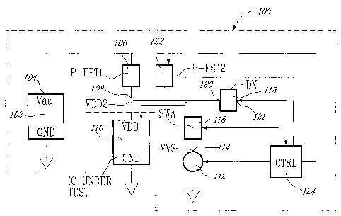
Turning now to Figure 3 of the appended drawings, a
Vddq IC testing system 100 according to a first embodiment of the present
invention will be described.
5 The testing system 100 includes a voltage source 102
having a known voltage output terminal Vaa 104, a resistive element P-
FET1 106 provided between the voltage output terminal Vaa 104 and a
node VDD2 108 to which an IC under test 110 is to be connected.
10 The system 100 also includes a controllable output
voltage source 112 having an output VVS 114 that may be connected to
the node VDD2 108 via a controllable switch element SWA 116, a
differentiator circuit 118 connected to the node VDD2 108 via an input
120, and a supplementary controllable switch P-FET2 122 connected
15 between the output terminal Vaa 104 and the node VDD2 108.
Finally, the testing system 100 includes a controller 124
connected to the voltage source 112, to the switch 116 and to the switch
122 to enable the adequate operation of these elements. The controller
124 is also connected to the IC under test 110 to sequentially supply test
vectors thereto. One skilled in the art would be in a position to determine
the number and nature of the test vectors to be applied before the testing
of a particular IC is completed.
It is to be noted that should the resistive element P-FET1
106 take the form of a Field Effect Transistor, it could be controlled by the
controller 124.
CA 02407766 2002-10-30
WO 02/42783 PCT/CA01/01636
16
it is also to be noted that the differentiator 118 has an
output 121 connected to the controller 124 to supply information about the
direction of the voltage variation as discussed hereinabove to allow the
controller to determine if the value of the voltage of terminal VVS should
be increased or decreased. For example, the differentiator 118 may
supply two different signals to the controller 124, a first signal indicating
that the voltage decreases and a second signal to indicate that the voltage
increases. The use of two different signals to indicate voltage increases
and decreases is advantageous for many reasons. First, it is possible to
select thresholds for voltage increases and decreases which allows a bias
to be introduced or not. Second, it may accelerate the entire process
when we are near the final voltage since neither signals would be emitted,
enabling the controller to stop the process. Third, it may be used to
reduce the noise.
Of course, the controller can be programmable and is
advantageously provided with instructions to carry out the method
described hereinabove with respect to Figures 1 and 2.
The operation of the test system 100 is believed to be
easily understandable by one skilled in the art after the understanding of
the corresponding method described hereina,bove.
The frequency of operation of the test system 100 is
advantageous since the system 100 implements the two strategies
described hereinabove to increase the testing speed. Indeed, the switch
P-FET2 is used to decrease the required time for the IC under test 110 to
reach its steady state and the controllable voltage source 112 is used in
CA 02407766 2002-10-30
WO 02/42783 PCT/CA01/01636
17
the successive approximation of the value of the voltage present at the
power supply terminal VDD by the increase or the decrease of the value
of WS.
Turning now briefly to Figure 4 of the appended drawings,
a more comprehensive diagram of the system 100 is illustrated.
As can be seen from this figure, the resistive element P-
FET1 106 is a resistor 126 and the supplementary controllable switch P-
FET2 122 is a P-type field effect transistor (FET). The controllable switch
element SWA116 takes the form of an analog switch.
Figure 5 of the appended drawings illustrates a Vddq IC
testing system 200 according to a second embodiment of the present
invention. Since the testing system 200 is very similar to the testing
system 100 of Figures 3 and 4, and for concision purposes, only the
differences between these two systems will be described hereinbelow.
The main difference between the systems 100 and 200
is that the system 200 includes three (3) controllable output voltage
sources 202, 204 and 206 having respective output terminals WS1, WS2
and WS3 having reference numerals 208, 210 and 212 connected to the
node VDD2 108 via respective controllable switching elements 214, 216
and 218.
Referring also to Figure 2, this arrangement of three
independently controlled output voltage source allows the controller 124,
while one of the source 202, 204 or 204 is adjusted to the predetermined
CA 02407766 2002-10-30
WO 02/42783 PCT/CA01/01636
18
initial value (in step 28), to adjust the other two sources to the increased
and decreased values of VVS (steps 42 and 40, respectively). The
system 200 is thereby ready to connect the adequate voltage source to
the node 108 in the next iteration of the method. As will easily be
understood by one skilled in the art, this feature further decreases the
testing time since it allows some of the steps of Figure 2 to be done
simultaneously.
As will readily be understood by one skilled in the art,
while the systems and method described herein measure the voltage at
the power supply terminal of the IC under test, the systems and method
of the present invention could easily be modified to measure the voltage
between the ground terminal of the IC under test and the electrical ground.
Although the presenfi invention has been described
hereinabove by way of preferred embodiments thereof, it can be modified,
without departing from the spirit and nature of the subject invention as
defined in the appended claims.