Note: Descriptions are shown in the official language in which they were submitted.
- - -. m..,........i .._.. ..... .. .......... ....__._ ....... .... .
CA 02408488 2009-03-31
TTI'LB OF THB IIWETTi'ION
[0001] Radio Frequency Detection and Identification System
BACKGROUND OF THB INVEN'I'ION
[0003] The present invention relates generally to radio frequCncy systems and,
more
particnlarly, to a radio frequency system for detecting resonant tags and for
ascertaining
information stored in the tags.
[0004] The use of radio freque,ncy systems for detecting and preventing theft
or
nnanrthorized removal of articles or goods from retail establislmnents and/or
other facilities, sach
as h'braries, has become widespread. In general, such seearity systems, lmown
generaIly as
elecdronic article security (SAS) systems employ a tag which is associated
with or which is
secm+od to the article to be protected. Tags may take on many diffez+ent
sizes, sbapes and forms
depeading upon the particnia type of 8AS system in use, the type and size of
the atticle, its
packaging, etc. In general, such BAS systeims are employed for dotecfmg the
presence of a tag
as the protectod article passes throngh or new a surveilled seamrity area or
zone. tn most cases, .
the survezlled scciuity area is loc,ated at or near an eagit or eatrance to
the retail establishmeait or
other facility.
10005] One snch etectrpnic article socatity system which has gained widespread
popnlaority
utibzes a tag whiah includes a resonant circuit which, when interrogated by an
electramagn~ic
field having prescn'bed characteristics, resonates at a single predeteainined
detection frequency.
When an article having an attached resonant tag moves into or otherwise passes
through the
sorveilled area, the tag is exposed to aai electromagnetic field created by
the security system.
Upon being exposed to the electromagnetic field, a ciment is induced in the
tag creating an
electromagnetic field which c6utges the electromagnetic field c=eated within
the sarveilled
area. The magnitude and phase of the cunvnt induced in the tag is a ftnction
of the proximity of
the tag to the security system, tho frequency of the applied electromagnetic
field, the resonant
frequency of the tag, and the Q factor of the tag. The resulting change in the
electromagnetic
-1-
CA 02408488 2002-11-07
WO 01/86967 PCT/US01/14463
field created within the surveilled area because of the presence of the
resonating tag can be
detected by the security system. Thereafter, the EAS system applies certain
predetermined
selection criteria to the signature of the detected signal to determine
whether the change in the
electromagnetic field within the surveilled area resulted from the presence of
a tag or resulted
from some other source. If the security system determines that the change in
the
electromagnetic field is the result of the presence of a resonant tag, it
activates an alarm to alert
appropriate security or other personnel.
[0006] While electronic article security systems of the type described above
function very
effectively, a limitation of the performance of such systems relates to false
alarms. False alarms
occur when the electromagnetic field created within the surveilled area is
disturbed or changed
by a source other than a resonant tag and the security system, after applying
the predetermined
detection criteria, still concludes that a resonaiit tag is present within the
surveilled area and
activates an alarm, when in fact no resonant tag is actually present. Over the
years, such EAS
systems have become quite sophisticated in the application of multiple
selection criteria for
resonant tag identification and in the application of statistical tests in the
selection criteria
applied to a suspected resonant tag signal. However, the number of false
alarms is still
undesirably high in some applications. Accordingly, there is a need for a
resonant tag for use in
such electronic article security systems which provides more information than
is provided by
present resonant tags in order to assist such electronic article security
systems in distinguishing
signals resulting from the presence of a resonant tag within a surveilled area
and similar or
related signals which result from other sources.
[0007] One method of providing additional information to the EAS system is to
provide a
tag which responds to the interrogation signal with a signal at a different
frequency than the
frequency of the interrogation signal or at more than one frequency.
Heretofore, single tags
having one of these properties required that the tag include an active element
such as a
transistor, or a non-linear element, such as a rectifier or diode, both of
which elements negate
manufacturing the tag as a planar passive device using the technology in place
for
manufacturing such resonant tags.
[0008] Another method of providing additional information to the EAS system is
to have
two or more resonant tags, each with a different resonant frequency, secured
to the article being
protected. For example, the resonant frequency of a second tag could be offset
from the
resonant frequency of a first tag by a known amount. In. this manner, the
simultaneous detection
-2-
CA 02408488 2002-11-07
WO 01/86967 PCT/US01/14463
of two or more signals at specific predetermined separated frequencies each
having the
characteristics of a resonant tag signal would have a high probability of
indicating the presence
of the multiple resonant tags in the surveilled area since the probability of
some other source or
sources simultaneously generating each of the multiple signals at each of the
predetermined
frequencies is very small.
[0009] The concept of utilizing a plurality of tags resonant at different
frequencies on each
article has not been generally accepted because of the requirement for
physically separating the
tags by a substantial distance in order to preclude the tags from interacting
in such a way that
the respective resonant frequencies are altered in an unpredictable way.
Placing the resonant
tags at a substantial distance from each other is disadvantageous because at
best it requires
separate tagging operations thereby substantially increasing the cost of
applying the resonant
tags. In addition, some articles are just not large enough to permit the two
or more tags to be
separated enough to preclude interaction. Separating the tags by a significant
distance also
affects the orientation and, therefore, the signal strength from the tags
thereby limiting
detectability of one or more of the tags.
[0010] There are also radio frequency systems, known generally as radio
frequency
identification (RFID) systems, which operate with resonant tags for
identifying articles to
which the resonant tag is attached or the destination to which the articles
should be directed.
The use of resonant circuit tagging for article identification is advantageous
compared to optical
bar coding in that it is not subject to problems such as obscuring dirt and
may not require exact
alignment of the tag with the tag detection system. Generally, the resonant
tags used in RFID
systems store information about the article by activating (or deactivating)
the resonant circuit
patterns which have been printed, etched or otherwise affixed to the tag.
Typically, systems
utilizing multiple tuned circuit detection sequentially interrogate each
resonant circuit with a
sigrial having a frequency of the resonant circuit and then wait for
reradiated energy from each
of the tuned circuits to be detected. The result of having to sequentially
interrogate the tag at
each of the different frequencies is a slow detection system that limits the
speed at which the
articles may be handled.
[0011] The present invention employs a tag having a plurality of resonant
circuits, each of
which are electromagnetically coupled to a receiving resonant circuit. Upon
interrogation by a
pulse at the receiving frequency, the tag radiates a detectable
electromagnetic signal having
frequency components which correspond to the resonant frequencies of the
resonant circuits.
-3-
CA 02408488 2002-11-07
WO 01/86967 PCT/US01/14463
Accordingly, the present invention is capable of reducing the false alarm rate
in EAS
applications without the need for separate tags with distinct frequencies
being placed on an
article; and also, is capable of providing information stored on the tag in
RFID applications.
BRIEF SUMMARY OF THE INVENTION
[0012] Briefly stated the present invention comprises a system for detecting
the presence of
an article comprising: a transmitter for radiating a first electromagnetic
signal at a
predetermined primary frequency; a resonant tag secured to the article, for
generating a second
electromagnetic signal in response to receiving the first electromagnetic
signal, the second
electromagnetic signal being at the primary frequency and at a predetermined
secondary
frequency different from the primary frequency; a receiver for receiving the
second
electromagnetic signal; and a computer connected to an output of the receiver,
said computer
processing the received second electromagnetic signal and generating an output
signal when the
secondary frequency is detected in the second electromagnetic signal.
[0013] The present invention further comprises a radio frequency system for
determining
the presence of information stored in a plurality of resonant circuits having
different resonant
frequencies, the system comprising: a transmitter for radiating a first
electromagnetic signal at a
predetermined primary frequency; a resonant tag, including the plurality of
resonant circuits,
each of the resonant circuits resonating at one of the different resonant
frequencies, -the tag
receiving the first electromagnetic signal and generating a second
electromagnetic signal in
response to receiving the first electromagnetic signal, the second
electromagnetic signal
comprising a plurality of secondary frequencies, each of the secondary
frequencies
corresponding to one of the resonant frequencies of the plurality of resonant
circuits; a receiver
for receiving the second electromagnetic signal; and a computer connected to
the output of the
receiver, said computer processing the received second electromagnetic signal
to detect the
presence of the plurality of secondary frequencies and generating an output
signal
corresponding to the information.
[0014] The present invention also comprises a method for detecting the
presence of an
article comprising the steps of: securing a resonant tag to the article;
transmitting a first
electromagnetic signal at a predetermined primary frequency; generating a
second
electromagnetic signal in response to the resonant tag receiving the first
electromagnetic signal,
the second electromagnetic signal being at the primary frequency and at a
predetermined
-4-
CA 02408488 2002-11-07
WO 01/86967 PCT/US01/14463
secondary frequency different from the primary frequency; receiving the second
electromagnetic signal; processing the received second electromagnetic signal;
and generating
an output signal when the secondary frequency is detected in the second
electromagnetic signal.
[0015] The present invention also comprises a method for determining the
presence of
information stored in a plurality of resonant circuits having different
resonant frequencies,
comprising the steps of: including the plurality of resonant circuits in a
resonant tag; radiating a
first electromagnetic signal at a predetermined primary frequency; receiving
the first
electromagnetic signal in the resonant tag and generating a second
electromagnetic signal in
response to receiving the first electromagnetic signal, the second
electromagnetic signal
comprising a plurality of secondary frequencies, each of the secondary
frequencies
corresponding to one of the resonant frequencies of the plurality of resonant
circuits; receiving
the second electromagnetic signal; processing the received second
electromagnetic signal to
detect the presence of the plurality of secondary frequencies; and generating
an output signal
corresponding to the information.
BRIEF DESCRIPTION OF THE SEVERAL VIEWS OF THE DRAWINGS
[0016] The foregoing summary, as well as the following detailed description of
preferred
embodiments of the invention, will be better understood when read in
conjunction with the
appended drawings. For the purpose of illustrating the invention, there are
shown in the
drawings embodiments which are presently preferred. It should be understood,
however, that
the invention is not limited to the precise arrangements and instrumentalities
shown.
[0017] In the drawings:
[0018] Fig. 1 is a schematic block diagram of a radio frequency detection and
identification
system in accordance with a preferred embodiment of the invention;
[0019] Fig. 2 is an electrical schematic circuit diagram of a dual-frequency
resonant tag in
accordance with a preferred embodiment;
[0020] Fig. 3 is a top plan view of a dual-frequency resonant tag having an
electrical circuit
equivalent to the electrical schematic circuit diagiram of Fig. 2;
[0021] Fig. 4 is a plot of the time domain response of a prototype of the
circuit of Fig. 2;
[0022] Fig. 5 is a plot of the frequency domain response of the prototype of
the circuit of
Fig.2;
-5-
CA 02408488 2002-11-07
WO 01/86967 PCT/US01/14463
[0023] Fig. 6 is a diagram illustrating the interrogation and response
characteristics of the
radio frequency system of Fig. 1;
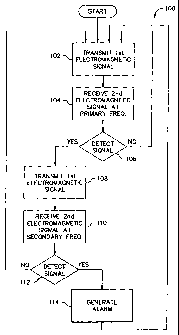
[0024] Fig. 7 is a flow diagram of the operation of the radio frequency system
for detecting
the presence of an article; and
[0025] Fig. 8 is a flow diagram of the operation of the radio frequency system
for
determining the presence of information stored in a plurality of resonant
circuits.
DETAILED DESCRIPTION OF THE INVENTION
[0026] Referring to the drawings, wherein the same reference numeral
designations are
applied to corresponding elements throughout the figures, there is shown in
Fig. 1 a schematic
block diagram of a preferred embodiment of an RF system 10 for detecting an
article and/or for
identifying infornzation about the article upon which a tag having specific
electromagnetic
characteristics has been attached. Preferably, the RF system 10 is of a type
called a pulse-listen
system, in which pulses of radio frequency (RF) electromagnetic energy having
a
predetermined pulse width, pulse rate and carrier frequency are radiated into
a detection and
identification zone. Following the radiation of each pulse into the detection
and identification
zone, the RF system 10 probes the electromagnetic field within the zone to
determine if a tag
having the specific electromagnetic characteristics is present in the
detection and identification
zone.
[0027] Preferably, the RF system 10 includes a transmitter 12 for radiating a
first
electromagnetic signal at one or more predetermined primary frequencies.
Preferably the
transmitter 12 includes a push-pull class D RF amplifier of a conventional
design generating a
pulse amplitude modulated signal having a pulse duration of approximately five
(5)
microseconds and having a carrier frequency in the range of 13.5 MHz. However,
as would be
appreciated by one skilled in the art, the carrier frequency of the output
signal of the transmitter
12 is not limited to 13.5 MHz. As contemplated, a transmitter operable at
carrier frequencies as
low as 1.5 MHz and as high as 7000 MHz. would be within the spirit and scope
of the
invention. Further, the pulse width of the pulse amplitude modulated signal is
not limited to
five (5) microseconds. As would be appreciated by those skilled in the art,
the pulse width of
the transmitter 12 would be selected to match the characteristics of the
specific tag used in the
RF system 10, such design choice being within the spirit and scope of the
invention.
-6-
CA 02408488 2009-03-31
[0028] The prefearod embodiment also includes a frequency synthesizer 52.
Preferably, the
$equency synthesizer is a digital frequency synthesizer similar to the digital
freqnency
synthesizer descrn'bed in U.S. Patent 6,232,878 eatitled "Reson,ant
Circuit Detection and Measureanent System Employing a Numerically Controlled
Oscillator".
The frequency synthesizer 52 provides a fust output signal for driving the
transmitter
12 at the primary frequency. The frequency synthesizer 52 also provides a
second output
signat for driving a conventionat mixea 40 portion of a supatheh+odyne
receiver 14. The
frequency of the second output signal of the froquency synthesizer 52 may be
the same as the
primary frequency or aiay be different fiom the primary fiequency (i.e. a
secondary frequency)
depending on the selected mode of opera.tion of the RF system 10, as discussed
below.
[0029] The RF system 10 also includes a dual-resonant tag 20 for receiving a
fQSt
elechumagnetic signal frm the transeoitter 12 and for generating a secamd
electrarnagnetic
signal in response to receiving the first electmmagnetic signal. The second
elealromagnetic
signal ceao4prises a frequeucy component wbieh corresponds to the primary
frequency of the
first electromagnet.ic signal and also a second frequency component whieh
corresponds to a
predetcrmined secandary frequency wbich is differeat from the primary f
requency.
[0030] Refaring now to Fig. 2 there is shown an electrical schematic
representstion of a
dual frequency tag 20 in accordance with a first prefened embodiment of the
present invention.
The dual frequency tag 20 includes four components namely, a f~rst' inductive
element or
inductanee Lp, a second inductive element or inductance L,s, a first
capacitive element or
capacitance Cp and a second capacitive element or capacitance Cs. The
aforementieaied
inductors and capacitors form a first resonant circuit which ie resonant at
the primary frequency
and a second resonant circuit which is resonant at the secondary firequency.
Preferably the first
and the socond resonent circuits ara electromagnetically coupled. Additional
inductive andlor
capacitive elements or components may be added if desired as shown by the
dashed lines in
Fig 2, and the cs?mpanents Ik. Ln and Ck, Cn to fonn ade8tioaai resonant
eirarits wbich are
electromagnetically coupled to the first magnetic circuit. As shown in Fig. 2
the second
indnctmce La is connected in series with the second capacitanee Cs. The first
capacitance Cp
is connected in parallel with the first inductance Lp. The sacies network (i.s
and Cs) is then
connected aeross the parallel network (Lp and Cp). Preferably, the inductors
Lp and Ls are
niagnetieally coupled to each other with a coupling coefficient K. However,
the coupling of the
-7-
CA 02408488 2002-11-07
WO 01/86967 PCT/US01/14463
first and second resonant circuits may also be accomplished by capacitive or
resistive coupling.
The values of the inductances Lp, Ls, the capacitances Cp, Cs and the coupling
coefficient K
are selected so that the dual frequency tag 20 as configured in Fig. 2 is
simultaneously resonant
at the first and second resonant frequencies.
[0031] Preferably, the resonant frequency of the first resonant circuit lays
in an Industrial,
Scientific and Medical (ISM) frequency band as assigned by the International
Telecommunications Union (ITU). Current ISM assigned bands include frequency
bands at 13,
27, 430-460, 902-916 and 2350-2450 MHz. Preferably, the resonant frequency of
the second
resonant circuit lays within a frequency band assigned to EAS systems,
currently including
approximately 1.95, 3.25, 4.75 and 8.2 MHz. In the preferred embodiment the
resonant
frequency of the first resonant circuit is at about 13.56 MHz. and the
resonant frequency of the
second resonant circuit is at about 8.2 MHz. Methods for selecting the values
of the
inductances and the capacitances to meet the frequency requirements of the
dual frequency tag
are well known to those of ordinary skill in the art and need not be described
herein for a
15 complete understanding of the present invention. The capacitances can be
lumped or
distributed within the inductances as will hereinafter be described.
[0032] Fig. 3 is a top plan view of the dual frequency tag 20 in accordance
with the
electrical circuit shown in Fig. 2. The dual frequency tag 20 is comprised of
a substantial
planar dielectric substrate 22 having a first principal surface or side 24 and
a second, opposite
20 principal surface or side 26. The substrate 22 may be constructed of any
solid material or
composite structure or other materials as long as the substrate is insulative,
relatively thin and
can be used as a dielectric. Preferably, the substrate 22 is formed of an
insulated dielectric
material, for example, a polymeric material such as polyethylene. However, it
will be
recognized by those skilled in the art that other dielectric materials may
alternatively be
employed in forming the substrate 22. As illustrated in Fig. 3, the substrate
22 is transparent.
However, transparency is not a required characteristic of the substrate 22.
[0033] The circuit components of the tag 20 as previously described are formed
on both
principal surfaces or sides 24, 26 of the substrate 22 by patterning a
conductive material. That
is, a first conductive pattern 28 (shown in the lighter color of Fig. 3) is
formed on the first side
24 of the substrate 22 which is arbitrarily illustrated in Fig. 3 as the
bottom or backside of the
tag 20. A second conductive pattern 60 (shown in the darker color on Fig. 3)
is formed on the
second side 26 of the substrate 22. The conductive patterns 28, 60 may be
formed on the
-8-
CA 02408488 2009-03-31
substrate surfaces 24,26, respectively with electrically conductive materials
of a known type
and in a manner wbich is well known to those of skill in the electronic ardcle
snrvei]lance art.
Preferably, the conductive material is patterned by a subtractive process
(i.e., etching) whereby
unwanted material is removed by chemical attack after the desired material has
been protected,
typically with a printed on etch resistant ink. In the prefened embodiment,
the conductive
matezial is ahuninum. However, other conductive materials (e.g., gold, nickel,
copper, bronzes,
brass, bigh density graphite, silver-filled conductive epoxies or the like)
can be substitated for
the aluminum without changing the nature of the tag 20 or its operation.
Similarly, other
methods (dye cutting or the h'ke) may be employed for forming the conductive
patterns 28, 60
on the substrate 22. The tag 20 may be manufactured by a process of the type
desc,n'bed in U.S.
Patent No. 3,913,219, entitled'Tlanar Circuit Fabrieation Pmcess".
However, other manufactturing processes can be used if desired.
100341 As previously stated, the first and second conductive patterns 28, 60
together form .
the resonant circuit as discussed above. In the embodiment as shown in Fig. 3,
both of the
inductances or inductive elements Lp and Ls are provided in the form of
conductive coils 62, 64
respectively, both of which are a part of the first conductive pattem 28.
Accordingly, both of
the inductsnces Lp and Ls are located on the fast side 24 of the substrate 22.
Preferably, the
two conductive coils 62, 64 are wound in the sme diredioo, as shown, to
provide a specified
amount of inductive coupling between them. In addition, first plates 66, 68 of
each of the
capacitive elements or capacitances Cp and Cs are formed as part of the f rst
conductive pattern
28 on the first side 24 of the snbstrate 22. Finally, seeond plates 70, 72 of
each of the
capacitances Cp and Cs are fomied as part of the second conductive pattern 60
and are located
on the second side 26 of the substrate 22. Prefarably, a direct electrical
connection extends
tlu+ough the substrate 22 to electrically connect the first caondactive
pattern 28 to the second
candactive pattern 60 to thereby continuously maintain both sides of the
substrate 22 at
substantially the same static charge level. Refeaing to Fig. 3, the first
conductive pattem 28
includes a generally square land 74 on the inner most end of the coil portion
62, which forms
the first inductance Lp. Likewise, a generally square land 78 is formed as
part of the second
conductive pattem 60 and is connected by a condudive beam 80 to the portion of
the seeaDd
conductive pattern 60, which fornns the second plate 70 of the furst
capacitance Cp. As shown
in Fig. 3 the conductive lands 74, 78 are aligned with each other. The direct
electrieal
comIection is made by a weld through ooimection (not shown), which e~ctends
between
-9-
CA 02408488 2002-11-07
WO 01/86967 PCT/US01/14463
conductive land 74 of the first conductive pattern 28 and conductive land 78
of the second
conductive pattern 60. Preferably, the direct electrical connection between
the lands 74, 78 is
formed by a weld in a manner which is well known to those of ordinary skill in
the EAS art.
[0035] Referring now to Fig. 4 there is shown a plot of the transient response
of a prototype
of the preferred embodiment of the dual frequency tag 20 after being radiated
with a pulsed
electromagnetic field having a five (5) microsecond pulse width and a carrier
frequency of
13.56 MHz. The prototype was designed to simultaneously resonate at both 13.56
MHz. and at
8.2 MHz. The prototype tag was placed at the center of a rectangular loop
antenna fabricated
from one (1) inch copper tape and was radiated by applying a radio frequency
(RF) signal to the
antenna. A probe connected to an oscilloscope was used to measure the residual
(ring-down)
electromagnetic field in the vicinity of the prototype tag when the
transmitted signal was
switched off. Fig. 4 clearly shows the presence of at least two frequency
components in the
time-domain ring-down signal. The time domain signal shown in Fig. 4 was
subsequently
transformed into the frequency domain by operating on the signal data with a
fast Fourier
transform (FFT). The result of applying the FFT to the data of Fig. 4 is shown
in Fig. 5, in
which obvious peaks in the frequency spectrum are shown at about 13.56 MHz.
and at about
8.2 MHz.
[0036] The preferred embodiment of the RF system 10 also includes a
superhetrodyne
receiver 14 of conventional design for receiving the second electromagnetic
signal from an
antenna 30 via an antenna switch 50 and a bandpass filter 32, and for
converting the received
RF signal to a baseband signal. The receiver comprises an RF amplifier 36, a
band pass filter
38, the mixer 40, a low pass filter 42 and an analog-to-digital converter 44.
The RF amplifier
36 and the band pass filter 38 have a bandwidth for covering the range of the
signals desired to
be detected. In the preferred embodiment, RF amplifier 36 and the bandpass
filter have a
bandwidth extending from about 5.0 MHz. to about 15Ø MHz. The bandpass
characteristic of
the RF amplifier 36 and the bandpass filter 38 could be a single substantially
flat bandpass
characteristic, a characteristic of multiple pass bands, or could be tunable
to a plurality of
narrower bandwidths depending on the design needs.
[0037] Preferably, the output of the bandpass filter 38 is connected to the
mixer 40. The
mixer 40 receives the output signal from the bandpass filter 38 and the second
output signal
from the frequency synthesizer 52 and converts the frequency of the output
signal of the
bandpass filter 38 to a baseband signal by multiplying together the output
signal of the
-10-
. ...b e,~. .. _ . ~.v.~ ...
CA 02408488 2009-03-31
bandpass filter 38 and the second output signal of frequency synthesizer 52.
The output of the
mixer 40 is filtered by the low pass filter 42 prior to applying the baseband
signal to the analog-
to-digital converter 44. The analog-to-digital converter 44 converts the
analog baseband signal
to a digital signal compatible with an input to a computer 46. As will be
appreciated by those
skilled in the art, the receiver 14 is not limited to aocepting an input
signal extending from
about 5.0 MHz. to about 15Ø MHz. As contemplated, a receiver capable of
receiving
fiequencies as low as 1.5 MHz and as high as 7000 MHz, is within the spirit
and scope of the
invention.
100391 The RF system further includes an antemia 30 for radiating the first
electromagnetic
sigaal and for providing the second electromagaetic signal received from the
tag 20 to the
receiver 14. Preferably, the amtenna is a loop antenna which provides a
detection and
: identificatioa zone in the near field proaimate tn the antetma 30 and
generalty provides for
c,ancellation of the electromagnefic field in the far field. A suitable
antanna is that disclosed in
U.S. Patent No. 5.602,556 entitled "Transmit and Receive Loop Antma".
However, other types of antemaas could be used. The
antenna 30 is connected to the transmitter 12 by the antenna switch 50 when
the timsmitter 12
is traasnnitting the first electromagnetic signal, i.e. dnring the "pulse
period" and is connected to
the receiver 14 when it is desired to receive the second elxtromagnetic
signal, i.e. during the
"hsten" period.
[0039] - The prefared embodiment of the RP system 10 finther includes a
computer 46
connected to an output of the receiver 14. The computer 46 processes the
received second
electromagnetic signal and genanates an output signal when a signature of the
reoaived second
electromagnetic signal meets a predatermined cariterlon As discussed below,
the criteria for
generating the output signal may include the detection of the secondary
$equency alone or may
inclnde the detection ofboth tha primmy frequency and the saeondary frequency.
Such
pmcessing for detecting the presence of resonant tags is well lcnown to tlmse
skilled in tLe art
and is not fiuther disclosed heereõ for the sake of brevity. The computer 46
also provides the
overall timing and control for the RF s.ystem 10. Preferably, the computer 46
comprises a
commercially available digital signal processor computer chip selected from
a.fmnily such ss
the T1VIS320C54X, available fim Texas Inshvmaits Corlwration, volatile random
access
memory (RAM) and noo-voladale read only memory (ROM). Computer executable
soflware
code stored in the ROM and axxeartmg in the eompukr chip and in the RAM
controls the RF
-11-
CA 02408488 2002-11-07
WO 01/86967 PCT/US01/14463
system 10 by providing control signals over control wires 34 to control the
frequency of the
frequency synthesizer 52, the pulse width of the output signal of the
transmitter 12 and the
position of the antenna switch 50.
[0040] Referring now to Figs. 6 and 7 there are shown a timing diagram and an
accompanying flow chart of a process 100 illustrating the operation of the RF
system 10 for
detecting a resonant tag 20 having two electromagnetically coupled resonant
circuits, in
accordance with the preferred embodiment. At times t0 to tl (step 102), the
computer 46
controls the frequency synthesizer 52 to generate a signal at the primary
frequency, controls the
antenna switch 50 to connect the transmitter 12 to the antenna 30 and gates
the transmitter 12
on to generate a pulse of RF energy to forrn the first electromagnetic signal
at the
predetermined primary frequency. From times t2 to t3 (step 104), the computer
46 controls the
antenna switch 50 to connect the antenna 30 to the receiver 14, thereby
preparing the receiver
14 to receive the second electromagnetic signal at the primary frequency. The
second
electromagnetic signal received by the receiver 14 at the primary frequency is
processed by the
computer 46 (step 106) to determine if the signal meets a predetermined
criteria which
characterizes the resonant tag 20 ring-down signal at the primary frequency,
such criteria being
stored in the computer 46. If the stored criteria for the ring-down signal is
met by the received
signal, the computer 46 retransmits the first electromagnetic signal at the
primary frequency at
times t4 to t5 (step 108). If the ring-down signal does not meet the
predetermined criteria, step
102 is repeated. At times t6 to t7 (step 110), the computer 46 controls the
frequency
synthesizer 52 to generate a signal at the predetermined secondary frequency
and controls the
antenna switch 50 to connect the receiver 14 to the antenna 30 to prepare the
receiver for
receiving the second electromagnetic signal at the secondary frequency. The
second
electromagnetic signal received by the receiver 14 at the secondary frequency
is processed by
the computer 46 (step 112) to determine if the signal meets a predetermined
criteria, also stored
in the computer 46, which characterizes the resonant tag 20 ring-down signal
at the secondary
frequency. If the stored criteria for the ring-down signal at the secondary
frequency is met by
the received signal, the computer 46 generates an alarm indicating the
presence of a resonant
tag 20 within the detection zone (step 114). If the ring-down signal does not
meet the
predetermined criteria, the process of detecting the resonant tag 20 returns
to step 102.
-12-
CA 02408488 2002-11-07
WO 01/86967 PCT/US01/14463
[0041] As will be appreciated by those skilled in the art, detecting the ring-
down signals
from the resonant tag 20 at botli the primary frequency and the secondary
frequency
substantially reduces the false alarm rate for an EAS system operating in an
interference
environment. However, as will be further appreciated by those skilled in the
art, it is not
necessary to detect the primary frequency and the secondary frequency
components of the
second electromagnetic signal sequentially, as described in the preferred
embodiment. The
primary and the secondary frequencies could be also be detected simultaneously
based on a
single transmission of the primary frequency. Further, detection of the
resonant tag 20 by
detecting only the primary frequency or only the secondary frequency alone is
possible and is
within the spirit and scope of the invention.
[0042] In practice, the resonant frequencies of the resonant circuits which
comprise the
resonant tag 20 have manufacturing tolerances which may result in the
frequencies of the ring-
down frequencies deviating from the predetermined primary and secondary
frequencies
sufficiently to degrade detection of the resonant tag 20. Preferably, the
first resonant circuit of
the resonant tag 20 is trimmed by a laser or other means so that the resonant
frequency of the
first resonant circuit is acceptably close to the predetermined primary
frequency. In this case,
the bandwidth of the receiver may be made narrow for detecting the primary
frequency and
wide for detecting the secondary frequency to allow for the tolerances of the
second resonant
circuit at the secondary frequency. Alternatively, the second resonant circuit
may also be
trimmed to be close to the predetermined secondary frequency.
[0043] In the cases where the first and/or the second resonant circuit of the
resonant tag 20
have an uncertainty of the resonant frequency which is undesirably large
compared to the
maximum acceptable RF bandwidth of the receiver 14, the following alternatives
are feasible:
[0044] a. Scan the frequency of the first electromagnetic signal over the
uncertainty range
of the first resonant circuit, as is commonly done for pulse-listen type of
EAS systems; when a
detection at the primary frequency is indicated, re-transmit the first
electromagnetic signal at
the indicated primary frequency and detect the second electromagnetic signal
at the secondary
frequency by: (1) employing an RF bandwidth in the receiver 14 which covers
the uncertainty
range of the second resonant circuit, (2) using a parallel bank of filters,
such as provided by an
FFT to cover the uncertainty range of the second resonant circuit, or (3)
continually
retransmitting the primary frequency and scanning the uncertainty range of the
second resonant
circuit.
-13-
CA 02408488 2002-11-07
WO 01/86967 PCT/US01/14463
[0045] b. Scan the frequency of the first electromagnetic signal over the
uncertainty range
of the first resonant circuit; for each transmission of the primary frequency:
detect the second
electromagnetic signal at the secondary frequency by: (1) employing an RF
bandwidth in the
receiver 14 which covers the uncertainty range of the second resonant circuit,
(2) using a
parallel bank of filters, such as provided by an FFT to cover the uncertainty
range of the second
resonant circuit, or (3) continually retransmitting the primary frequency and
scanning the
uncertainty range of the second resonant circuit.
[0046] The present invention is not limited to merely detecting the presence
of a resonant
tag 20 in a detection zone by detecting the ring-down of one or two resonant
circuits as for an
EAS surveillance function. The present invention also includes within its
scope a radio
frequency identification (RFID) capability which employs a single tag having
two or more
resonant circuits, (see Fig. 2), with each resonant circuit being designed to
resonate at a
different frequency. Such a tag would have a single first resonant circuit
resonant at a primary
frequency and a plurality of second resonant circuits, each of which second
resonant circuits
resonating at a different frequency and each of such second resonant circuits
being
electromagnetically coupled to the first resonant circuit. For example, the
resonant tag 20 could
include a first resonant circuit at the primary frequency and four different
second resonant
circuits, each resonating at a different resonant frequency within the
detection range of
associated equipment. By identifying the particular frequencies at which the
various resonant
circuits of the tag resonate, it is possible to obtain identification
information from the tag.
[0047] In the presently preferred embodiment, the preferred detection
frequency range
extends from about 10 MHz to about 30 MHz. However, any other frequency range
could be
used. Using state of the art manufacturing equipment, it is possible to
produce, in commercial
quantities, an inexpensive radio frequency identification tag having two or
more resonant
circuits thereon to establish a unique signature with the resonant frequency
of each resonant
circuit being controllable so that the resonant circuit resonates at a
predetermined frequency
with an accuracy of plus or minus 200 KHz. In this manner, within the
detection frequency
range of 10-30 MHz, it is possible to have up to 50 resonant circuits, each of
which resonates at
a different frequency without overlapping or interfering with one another.
Thus, assuming a tag
with four separate resonant circuits, the first resonant circuit could
resonate at a first selected
frequency within the detection frequency range, for example, 14.4 MHz leaving
49 available
frequencies within the detection frequency range for the other three resonant
circuits of the tag.
-14-
CA 02408488 2002-11-07
WO 01/86967 PCT/US01/14463
The second resonant frequency could then be selected to resonate at a second
frequency within
the detection frequency range, for example, 15.6 MHz leaving 48 possible
frequencies for the
other two resonant circuits of the tag. The third resonant frequency could be
selected and the
tag fabricated to resonate at a third frequency, for example, 20 MHz leaving
47 possible
frequencies for the fourth resonant frequency. The fourth resonant frequency
could then be
selected and the tag fabricated to resonate at a fourth frequency, for
example, 19.2 MHz. A tag
having four specifically identified resonant frequencies and a unique
signature when
interrogated could then be assigned a particular identification number.
Because of the number
of potential frequencies within the detection frequency range, a tag having
four resonant
circuits thereon, each with a different frequency, is capable of having
approximately, 5.2
million combinations or approximately 22 bits of data.
[0048] Fig. 8 is a flow diagram of a preferred process 200 for using the RF
system 10, as
shown in Fig. 1, for identifying the resonant frequencies of the RFID tag by
interrogating the
tag at the primary frequency of the RFID tag and by detecting the presence or
absence of a
predetermined ring-down signature at each of N secondary resonant frequencies.
At step 202
the computer 46 controls the frequency synthesizer 52 to generate a signal at
the primary
frequency, controls the antenna switch 50 to connect the transmitter 12 to the
antenna 30 and
gates the transmitter 12 on to generate a pulse of RF energy to form the first
electromagnetic
signal at the predetermined primary frequency. At step 204, the computer 46
controls the
antenna switch 50 to connect the antenna 30 to the receiver 14, thereby
preparing the receiver
14 to receive the second electromagnetic signal at the primary frequency. The
second
electromagnetic signal received by the receiver 14 at the primary frequency is
processed by the
computer 46 (step 206) to determine if the signal meets a predetermined
criteria which
characterizes the resonant tag 20 ring-down signal at the primary frequency,
such criteria being
stored in the computer 46. If the stored criteria for the ring-down signal is
met by the received
signal, the computer 46 sets a counter to the integer number "one" (step 208)
and retransmits
the first electromagnetic signal at the primary frequency (step 210). At step
212, the computer
46 controls the frequency synthesizer 52 to generate a signal at the Kth
predetermined
secondary frequency and controls the antenna switch 50 to connect the receiver
14 to the
antenna 30 to prepare the receiver for receiving the second electromagnetic
signal at the Kth
secondary frequency. The second electromagnetic signal received by the
receiver 14 at the
secondary frequency is processed to detennine if the signal meets the
predeterniined ring-down
-15-
CA 02408488 2002-11-07
WO 01/86967 PCT/US01/14463
signature criteria and a result of the processing is stored by the computer 46
(step 214). At step
216 the current value of the counter is compared with the number "N" which
represents the
number of secondary frequencies to be received. If the value K of the counter
is less than N,
the process 200 is continued at step 210. If the value K of the counter is
equal to N the process
200 is completed by reporting which secondary frequencies were received having
the
predetermined ring-down signature (step 218), and the RFID process 200 is
started again at step
202.
[0049] In summary, the present invention provides a system and a method for
interrogating
a resonant tag at a single (primary) frequency and for receiving information
stored in the tag by
one or more resonant circuits which are resonant at frequencies other than the
primary
frequency. Accordingly, the present invention provides a means for reducing
the false alarm
rate of an EAS system and a means for interrogating an RFID tag to receive
information stored
in the tag by radiating electromagnetic energy at only the single (primary)
frequency.
[0050] It will be appreciated by those skilled in the art that changes could
be made to the
embodiments described above without departing from the broad inventive concept
thereof. It is
understood, therefore, that this invention is not limited to the particular
embodiments disclosed,
but it is intended to cover modifications within the spirit and scope of the
present invention as
defined by the appended claim
-16-