Note: Descriptions are shown in the official language in which they were submitted.
CA 02410203 2002-11-22
WO 01/93048 PCT/USO1/17532
MODEM HAVING FL'E~IBLE ARCHITECTURE
FOR CONNECTING T4 MULTIPLE CHANNEL INTERFACES
RELATED APl?LICATIONS
The present invention claims priority to U.S, Provisional application no.
601207,955,
filed May 31, 2000, whose contents are incorporated by reference.
FIELD OF THE 1NVENTTON
The present invention generally relates to a communications modem. More
specifically, the present invention relates to a comxnunicatiops modem which
can be
interfaced to number o~ different channels.
HACRGROUND OF TFIE INVENTION
1$ Digital Subscriber Line (xDSL) is a technology which allows for
simultaneous voice
and data txaffc to coexist over a communication channel comprising a standard
telephone
transmission line. Typically, a standard telephone. transmission line
comprises an
unshielded twisted pair of copper wire having a gauge of 22-2bAWC7, Twisted
pairs,
which can be used to connect a central telephone system (a 'central' unit) to
a subscriber's
telephone (a'remote' unit) can support bandwidths of up to ZMHz through the
use of digital
signal processing (DSP) technology. Thus, they can be used for bandwidth-
intensive
applications, such as Internet access and video-on demand, as well as for
carrying voice
traffic. Frequency division multiplexing is used so that a plurality of
signals, each
occupying a different frequency band, can be simultaneously sent over the same
txansznissian line.
The voice traffic band comprises a number of frequency sub-bands, or channels,
ranging from DC to 20 K.Hz. The analog voice band frequency is typically
specified as
200-4000 Hz. Customer specified additions may include phone operation up to 8
l;Hz in
addition to 12-16 KHz billing tones. In addition, DC to 30 I!z frequencies are
typically
assigned for auxiliary axialog signaling purposes, such as ringing the
telephone, dial pulsing
and onloff hook signaling.
ADSL data traffic bandwidth for Discrete Multitone (DMT) modulation is
typically
from 25 KHz - I .1 M>;iZ. Of this, upstream data traffic (i.e., remote unit to
central unit)
uses the 25 KHz-138 KFIz band, while the downstream traffic (i.e., central
unit to remote
unit) uses the 138 KHz-1.1 MHZ band.
-1-
CA 02410203 2002-11-22
WO 01/93048 PCT/USO1/17532
U.S. Pat. No. 5,541,955 discloses an adaptive data rate modem. The modem
incorporates an adaptive data rate encoder and an adaptive data rate decoder
using adaptive,
parallel-branch decoding to translate received symbols into corresponding data
bits. The
data rate is changed automatically and dynamically without interrupting the
decoding
process. A constant channel symbol rate and a single signal set simplify
signal acquisition
and synchronization. Tncoming and outgoing data are buffeted, and the
transmission rate is
changed dynamically by a memory controller to avert buffer overflows and
undertows. An
optional adaptive phase-lock loop system maintains synchronization of the
decoder at all
data rates.
U.S. Pat. No. 5,841,540 discloses a multiple line modem and method enabling a
user
to automatically usurp a plurality of telephone lines for data transfer when
the telephone is
not in use. A user is able to switch from multiple line data operation to one
(or more) line
data and one (or more) line telephone operation automatically when the
telephone handset is
lifted or an incoming call is detected signaling a request for voice service.
The multiple line
1.5 modem automatically reestablishes the data connection on the lines) that
was used for
voice service when the voice SeNice terminates. The multiple line modem allows
end to
end service that is transparent to the central office. When all lines are
operating in data
transfer mode, the aggregate data transfer rate is multiplied by the number of
lines available
for data transport. When one line{s) is operating in voice service mode, the
other lines)
2D maintains data transfer operation at a reduced rate. The lines) that is
used for voice service
is adaptively managed by the multiple line modem to provide seamless switching
between
data transfer mode operation when voice service is not requested and voice
service mode
operation when voice service is requested.
U.5. Pat, No, 5,910,959 discloses a methodology for a modem control channel.
The
25 channel allows faster seamless rate change and precoder tap ehchange than
the baseline
procedure for seamless rate change, allowing for more robust transmission of
control
information. Zt can also be used to convey side-information in the. case of
multiple data
applications, serving the purpose of mode switching. Thus, with a single
control channel
both the needs for seamless rate change and transmitting control information
for multiple
30 data applications can be met.
U.S. Pat. No, 6,002,722 discloses a modem operating selectively in the voice
fzequency and higher fxequency bands which supports multiple line codes. A DSP
is used
to implement different existing ADSL line codes on the same hardware platform.
The
modem negotiates in real time for a desired line transmission rate to
accommodate line
3S condition and service cost requirements which may be implemented at the
beginning of
_z_
CA 02410203 2002-11-22
WO 01/93048 PCT/USO1/17532
each corxununication session by exchange of tones between modems. A. four step
MDSL
modem initialization process pzovides line code and rate compatibility, The
handshake
protocol and receiver algorithm allow reliable modem synchronization over
severely
amplitude distorted channels and makes use of a short length sequence to train
a
synchronizing equalizer at the receiver. The algorithm and corresponding
training sequence
to train the transmitter filtez are provided. A.ftex training to this
seduence, a matched filter
or correlatox detects the inverted sync sequence. Detection of the invented
sequence signals
commencement of normal reference training of the demodulation equalizers. An
internal
state machine in an MDSL modem records and monitors line status and notifies
state
change to other MDSL and host processor. The protocol fox exchanging line
connection
management messages is a simplified LCP for MDSL. In a DMT system, a
transmitter filter
reduces the length of effective channel impulse response. Implementation of
the filter
combines time domain convolution and frequency domain multiplication to reduce
needed
computation power. The filter coefficients update may occur through a feedback
channel.
The contents of aforementioned U.S, Pat. No. 5,541,955, U.S. Pat. No.
5,8?4,840,
U.S. Pat, No. 5,910,959, and U.S. Pat. No. 6,002,722 axe incorpozated by
reference to the
extent necessary to understand the present invention.
SUMMARY OF TI-IE INVENTION
The present invention is directed to an xDSL modem including a controller
having a
computer memory associated therewith, wherein the controller is configured to
simultaneously support both a wireless Local Area Network (LAN) and a home
phoneline
networking alliance (HPNA) connection.
The present invention is also directed to an xDSL modem comprising a
controller
having a computer memory associated therewith; software resident in said
computer
memory, said software comprising pxeloaded software drivers configured to
support a
plurality of PCMCIA cards; at least one PCMCTA slot accessible from an
exterior surface of
the modem; and at least one port configured to accept a new software driver
suitable for
cooperating with a PCMCIA card for which no suitable software driver is
already resident
in said computer memory, wherein upon insertion of a PCMCIA card, a proper
softwaze
driver is automatically invoked, if said proper software driver is resident in
said computer
memory.
The present invention is further directed to an xDSL modem comprising a
motherboard having a controller having a first computer memory associated
thezewith; and
at least one voice expansion slot connected to the motherboard; wherein the
xDSL modern
-3-
CA 02410203 2002-11-22
WO 01/93048 PCT/USO1/17532
is conveztible into a voice-capable device, upon insertion of a voice card in
the voice
expansion slot. Such an xDSL modem may further comprise a voice card
comprising at
least one digital signal processor (DSP) unit and at least one subscriber line
interface
circuits (SLIC), the voice card being configured to support at least one coder-
decoder
(codec) standard and at least one voice protocol. In addition, the codec
standard may
include standards from the group consisting of Cy.71 l, 6.726, 6.723.1, G.729A
and 6.728,
while the voice protocol may include standards from the group consisting of
MGCP, SIP,
H,323, H,248/MEGACO.
The present invention is also directed to an xDSL modem comprising a wireless
Local Area Network (LAN) connection, a home phaneline networking alliance
(HPNA)
connection an ethemet connection, an universal serial bus (USB) connection.
Additional
features may include one or more PCMCIA slots, a voice expansion slot, an
audio port; and
a serial port.
BRIEF T~ESCRTPT10N OF TI-IE DRAWINGS
The present invention is described in detail below with reference to the
drawings in
which;
FIG, 1 presents a block diagram of an access system which incorporates an
integrated access device (TAI?) in accordance with the present invention;
FIG. 2 is a front perspective view of one embodiment of the access device
according
to the present invention;
FIG. 3 is a reaz view of one embodiment ofthe access device according to the
presentinvention;
FIG. 4 is a close-up view of a portion of the. rear view of one embodiment of
the
access device according to the present invention;
FZG. 5 shows an Ethernet network with an access device according to the
present
invention;
FIG. 6 shows an HPNA network with an access device according to the present
invention;
FIG. 7 shows a wireless network with an access device according to the present
invention;
FIG. ~ shows a hybrid network with an access device according to the present
invention;
-4-
CA 02410203 2002-11-22
WO 01/93048 PCT/USO1/17532
FIG. 9 is a block diagram of one embodiment of the access device in accordance
with the present invention;
FIG. 10 is a block diagram of another embodiment of the access device in
accordance with the present invention;
FIG. 11 shows an access system which incorporates an access device according
to
the present invention with a POTS splitter;
FIG. 12 shows an access system which incorporates an access device according
to
th.e present invention with microfilters;
FIG. 13 shows a sample an-screen installation instructions window;
FIG. 14 shows a sample home page of the access device containing on-line
configuration instructions fox a usez to configure the access device; and
FIG. 15 is a flow chant summarizing the installation procedure and use ofthe
access
device according to the present invention.
DETAILED DESCRIPTION OF PREFERRED EMBODIMENTS
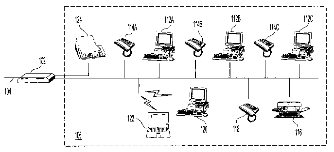
FIG. 1 is a block diagram of an access system which incorporates an integrated
access device (IAD) in accordance with the present invention. As shown in FIG.
I, the
access system 100 comprises an access device 102, a transmission line 104
which is
connected to the access device 102, and a network 106 which is also connected
to the access
device 102. The transmission line 104 can be a single digital subscriber line
(DSL) litre.
The access device 102 is an TAD. It allows users to physically network
multiple client
computers and phones together to share a single DSL line and Inteznet
connection. As
shown in FIG. l, the network 106 connects a plurality of computers 1 I2A,
112B, and 1 I2G,
such as personal computers (PCs), a plurality of telephone equipment 114A,
1148, and
2~ 114C, such as telephone sets and FAX machines 124, ancillaries 116 such as
printers and
scanners, IP phone 118, such as VoIP (voice over Internet protocol
(IP)),'VoDSL (voice
over DSL), and VoATM (voice over asynchronous transfer mode (ATM)). The
network
106 can also he wirelessly connected to remotely located computers I20 and
mobile
computers 122 such as laptops and personal data assistants (PDAs).
FIG. 2 is a front perspective view of one embodiment of the access device
according
to the present invention. In the access device 200 shown in FIG. 2, theze is a
plurality of
Light Emitting Diode (LEDs) and two personal computer memory card intematianal
association (PCMCIA) card ports.
At the front is a LED panel 202, located on which are a power LED 204, a DSL
LED 206, a first PCMCIA LED 208, a second PCMCIA LED 210, and an aetivifiy LED
-5-
CA 02410203 2002-11-22
WO 01/93048 PCT/USO1/17532
group 212. These LEDs, as will be discussed in detail below, indicate the
status and
activities of various components of the access device 200. Located on one side
of the
access device 200, as shown in FIG. 2, is a port panel 214, which contains a
first PCMCIA
port 216 and a second PCMCIA port 218. These two ports receive PCMCIA cards,
including PCMCIA cards that support wireless eomxnunieations such as for
establishing a
virtual private network (Vl'N).
The power LED 204 indicates the application of power to the access device 200.
When power is on, the power LED 204 shows green light. Otherwise, when the
power is
off, the green light is off. The DSL LED 206 indicates the DSL connection and
the
synchronization with asymmetric DSL (ADSL) transceiver unit (ATU). When DSL is
connected and is synchronized with ATU-C (ATU central), the DSL LED 206 shows
green
light. When DSL is connected and is not synchronized with ATU-C, the DSL LED
206
shows yellow light, When there is no bSL connection, the DSL LED 206 shows no
light.
The first PCMC1A LED 208 indicates the status of the first PAMCIA port 216.
When
pCMCIA port 21; 6 has a PCMCIA card glugged in, the PCMCIA LED 208 shows green
light. Otherwise, when PCMCIA port 216 does not have a pCMCIA card plugged in,
the
pCMCIA LED 208 shows no light. Similarly, the second PCMCIA. LED 210 indicates
the
status of the second PAMCIA port 218. When PCMCIA pozt 218 has a PCMCIA card
plugged in, the PCMGTA LED 210 shows green light, Otherwise, when PCMCIA port
218
does not have a PCMCIA card plugged in, th,e PCMCIA LED 210 shows no light,
Finally,
the activity LED group 212 comprises a plurality of LEDs to indicate the
activity of the
access device 200 on a 0-100% scale. Preferably, there axe 6 LEDs, with the
one on the left
lighting up most frequently even if there is little activity and the one on
the right lighting up
only when the activity reaches near 100°t°. Table I summarizes
the indication of all the
LEDs on the LED panel 202 of the access device 200.
k'IG. 3 is a rear view of one embodiment of the access device according to the
present invention. In the access device 300 shown in PIG. 3, at the rear side
is a connection
panel 302, A plurality of ports and slots aze located on the connection panel
302 for
connections. Power adapter port 304 accepts a power cord, preferably with 24V
AC
transformer, and is controlled by power switch 306. DSL port 308 receives a
DSL
transmission line. $thernet port 310 comprises 4 Ethernet hubs for wired
networking with
computers. USB slot 312 is for universal serial bus (USB) connection with
computers and
its connection status is indicated by USB link LED 314. When there is a USB
connection, a
USH link LED 314 shows gze.en light. Otherwise, when there is no USH
connection, the
US$ link LED 314 shows no light. Duo! HPi'~IA port 316 is for home phoneline
networking
-6-
CA 02410203 2002-11-22
WO 01/93048 PCT/USO1/17532
LED No Light Color Light
power LED 204 power off green power on
DSL LED 206 tto DSL connectiongreen DSL connected and
(dual
color) synchronized with
ATU-C
yellowDSL connected and
but not
synchronized with
ATU-C
first PCMCIA first PCMCIA green first PCMCIA card
LED card not
208 plugged in plugged in
second PCMCIA second PCMCIA green second PCMCIA card
card
LED 2.10 not plugged in plugged in
activity LEDs no activity green activity on a 0-100%
212 scale
Table 1: Indications of LEDs on the LED panel.
alliance (H'PNA) connection. It comprises a first jack 316b far phone
connection and a
second jack 316a for line connection, with their connection status indicated
by an HPNA
link LED 318 and their activity status indicated by an HPNA activity LED 320.
When there
's ~ HPNA connection, the HPNA link LED 318 shows green light. Otherwise, when
there
is no HPNA connection, the HPNA link LED 318 shows no light. Also, when there
is an
IIPNA connection, the HPNA activity LED 320 flashes green light in a frequency
relative to
the intensity of the activities over the HPNA connection. Serial port 322 is
for connection
to telemetry service input, The telemetry service includes remote control,
among other
functionalities. Voice slot 324 is for telephony service input. Prefezably, it
comprises up to
4 RJ-11 connections. The telephony service includes VoIP (voice over IP) and
VoATM
(voice aver ATM). Audio-in port 326 is for music.-on-hold input. The
indications of the
LEDs of the connection panel 302 shown in FIG. 3 and FIG, 4, below, are
summarized in
Table 2. It is understood that the lights, slots, connections and other
features may appear
on p~'els axed surfaces of the access device othez than the ones in the
preferred embodiment.
FIG. 4 is an enlarged view of a portion of floe rear view of one embodiment of
the
access device according to the present invention. As shown in FIG. 4, located
below a
voice slot 424 is an Ethernet port 410, which comprises 4 Ethernet hubs 412,
414, 416, and
418. There are four Ethernet link LEDs 402 and four Ethernet activity LEDs
404. For each
E~emet hub, an Ethernet link LED 402 indicates its link status and an Etheznet
activity
LED 404 indicates its activity status. When there is art Ethernet connection
at az~ Ethemet
CA 02410203 2002-11-22
WO 01/93048 PCT/USO1/17532
hub, the associated Ethernet link LED 402 shows green light. Otherwise, when
there is no
Ethemet connection at the Ethemet hub, the associated Ethemet link LED 402
shows no
light. Also, when there is an Ethernet connection, the associated Ethernet
activity LED 404
flashes yellow light in a frequency relative to the intensity of the
activities over the Ethernet
S connection. The indications of tl~e LEDs of the cormection panel 302 shown
in FTG. 4 and
p'IG. 3, above, are summarized in Table 2. It should be noted that other
numbers of
Ethernet hubs may be provided.
LED No Light Color Solid Light Flashes
US13 link no USB connectiongreen USB connected NIA
LED
3I4
HPNA lintlc.no 1-IPNA connectiongreen HPNA connected NIA
LED
318
I HPNA activityno activity green NIA. activity
S
LED 320
Ethernet the associated green the associated NlA
link
LED 402 Ethernet hub Ethemet hub
not
connected connected
Ethernet no activity yellowNIA TxIRx
activity
LE1J 404 activity
Table 2: indication of LEDs on the connection panel.
With the capacity of providing a variety of options, an access device in
accordance
wi.~ ~e present invention can satisfy different users having different needs.
For example,
for home networking, the access device 200 provides Internet access to
multiple users
simultaneously over a single telephone line, while retaining the benefit of
bringing voice
service to the home on the same telephone line as the Internet service. For
small office
networking, the access device 200 provides multiple local area network (LAN)
options with
multiple interfaces, such as Ethernet, T-IPNA, and wireless LAN (WLAN), all
over a single
ADSL connection. For home offtce or telecornmuting, the access device 200
provides
virtual private networking (VPN), separates FAX and voice lines, and brings
private branch
exchange (PBS functions.
F1G, 5 shows an Ethemet network with an access device according to the present
~5 invention. As shown. in FIG. 5, the Ethernet network 500 comprises an
access device 502, a
_g,
CA 02410203 2002-11-22
WO 01/93048 PCT/USO1/17532
plurality of computers, shown generally as 504, and at least one peripheral
506. Each of the
plurality of computers 504 is coz~meeted to an Ethernet hub on the access
device 502. The
peripherals 506 can be devices such as printers and scannezs and are connected
to the
computers 504, The access device 502 is connected to a single DSL line 510
through which
DSL services are provided by a DSL service provider, shown generally as 508.
In the
Ethernet network 500, each computer 504 has DSL access through the single DSL
line 5I0.
Also, each computer 504 has access to shared files and peripherals 506.
Prefezably, the
access device has up to four wired Ethernet connections. Additional computers
may be
added through the use of additional Ethernet hubs.
I O FIG. 6 shows an HPNA network with an access device according to the
present
invention. As shown in FIG. 6, the HPNA network 600 comprises an access device
602, a
plurality of computers 604, and peripherals 606. Each computer 6Q4 is
connected to the
access device 602 via a telephone Line 618. A dual jack 6I6 receives input
from a single
DSL transmission Iine 610 fihrough which DSL services are provided by a DSL
service
provider 608. The dual jack 616 is connected to the access device 602 via both
an HPh3A
line 612 and a DSL connection line 614. In the HPNA network 600, each computer
604 has
DSL access over the single DSIJ line 610. Also, each computer 604 has access
to shared
files and peripherals 606.
FIG. 7 shows a wireless network 700 with an access device 702 according to the
present invention. As shown in FIG. 7, the wireless network 700 comprises an
access
device 702 and a plurality of computers 704. Each computer 704 is connected to
the access
device 702 by radio signals transmitted and received by a radio transmitter
720 attached to
each computer 704. The access device 702 is connected to a single DSL line 710
through
which DSL services are provided by a DSL service provider 708. Also, a PCMCIA
card
with Wireless LAN (WLAN) capabilities is plugged into the access device 702 to
enable the
access device 702 to use the radio signals. Preferably, the PCMCIA card uses a
borne radio
frequency (HRF) card. In the wireless network 700, each computer ?04 has DSL
access
over the single DSL line 710,
FIG. 8 shows a hybrid network 800 with an access device 802 according to the
present invention. It is a network which combines the features of the Ethernet
network of
FIG. S, tl~e HPNA network of FIG. 6, arzd the wireless network of FIG. 7. In
addition, it
also involves the use of the USB connection of the access device. As shown in
FIG. 8 the
hybrid network 800 comprises an access device 802, one or more Ethezxiet-
enabled
computers 804a, one or more HPNA-enabled computers 804b, one or more wireless-
enabled computers 804c, a USB-enabled computer 804d, and peripherals 806. The
Ethemet
computers 804a are computers connected to the Ethemet hubs on the access
device 802, the
_g_
CA 02410203 2002-11-22
WO 01/93048 PCT/USO1/17532
HPNA computers 804b are computers connected to the HPNA connections via a
telephone
line 818 on the access device 802, the USB corrlputer is a computer connected
to the USB
connection of the access device 802, and the wireless computers 804c are
computers
connected to the access device 802 via radio or even light signals. The
peripherals 806 are
connected to the computers. A dual jack 816 receives input from a single DSL
transmission
line 810 through which DSL services are provided by a DSL service provider
808, The dual
jack 816 is connected to the access device 802 via both an FIPNA line 812 and
a DSh
connection line 814. In the hybrid network 800, each computer has DSL access
through the
single DSL line 810. Also, each computer has access to shared files and
peripherals 806,
FTG. 9 is a block diagram of one embodiment of the access device in accordance
with the present invention. It shows the major components on the mother board
of the
access device. As shown in FZG. 9, access device 900 comprises a DSL jack 9a2,
a DSL
line interface 90~, and an xDSL transceiver 906. The DSL jack 902, DSL line
interface
904, and xDSL transceiver 906 function as an ADSL transceiver unit (ATU) and
support IP
forwarding (routing) and point-to-point protocol {PPP). The DSL jack 902
receives a DSL
line. The DSL line interface 904 interfaces with DSL signals Coming from the
DSL line. Xt
may also function as a POTS {plain old telephone system) filter. The xDSL
transceiver 906
is a netwozk adapter which transmits and receives the DSL signals. It also
supports
software dowxlloading. Having the functions as an ATU and those that will be
discussed in
detail below, the access device acts as a bSL modern and combines the
functions of a
gateway, router, and Ethernet hub to provide high.speed Internet access to PCs
sharing a
local netwozk. It provides point-to-point protocol over Ethemet (PPPOE)~
tunneling through
network address translation (NAT). Preferably, the I3SL jack 902 is a
registered jack-45
(Rf-45) and the xDSL transceiver 906 is an ALCATEL~ ADSL DMT chipset (MTIC-
20140). DSL line interface is well known in the art. Table 3 lists the
preferred products for
the major components shown in FIG. 9, except those well known in the art. In a
preferred
embodiment, the DSL jack 902 corresponds to the DSL port 308 of FICr. 3.
The access device 900 also comprises PCMCIA sockets 910 for acceptance of
PCMCIA cards, flash memory 912 into vyhich software drivers and the like may
be stored or
;p downloaded, and SDRAM 914. These components constitute a PCMCZA interface
and
function to receive and service PCMCIA cazds, This PCMCIA interface preferably
supports
16 bit type-II PCMCIA cards. It also support Bluetooth and other protocols.
Supported
1'CMCIA cards include conventional PC cards, such as streaming video and video
capture
cards, as well as WLAN cards, such as Eluetooth, IEEE802.1 la, FEEE802.1 lb,
HomeRF,
- 10-
CA 02410203 2002-11-22
WO 01/93048 PCT/USO1/17532
Component Preferred product
DSL jack 902 R1-45 jack
~.DSL transceiver ALCATEL~ ADSL DMT chipset (MTK-20140}
906
FPGA 908 Altexa~ gate array
PCMCLA sockets 910 standard 64 pin sockets
flash memory 912 SHARP~ 32 Mb flash memory
SDRAM 914 SHARPS 16 Mb SDRAM
miarocontroller 918 Motorola~ M855 processor
serial connector 922 dual RS-232 connector
LAN repeater 926 Hex repeater with 6 ports
Ethernet jacks 930 Quad Integrated RJ-45 jacks
USB port 932 Type-H USB
HPNA port 934 telephone jack
LAN oscillator 940 25 MHz oscillator
microcontroller oscillator3-5 MHz oscillator
946
Table 3: The pzefezred products for the major coimponents shown in F1G, 9.
HiperLAN, HipexLAN2, and RadioLan 10 Mbps WLAN PCMCIA, cards. Listed in Table
4
axe some o~the applications supported by the PCMCIA interface. Also, listed in
Table 5
are some of the modes of operation supported by the PCMCIA interface,
Preferably, the
number of sockets in PCMCL~1 sockets 910 is 2, the PCMCIA sockets 910 are
standard 64
pin sockets, the flash memory 912 is a SHARPS 32 Mb flash memory, and the
SDRAM 914
is a SHARP'S 16 Mb SDRAM. In a prefezxed embodiment, the PCMCIA sockets 910
correspond to the ~zst and second PCMCIA ports 216 and 218 of FIG 2. The
PCMCIA
cards can be plugged and unplugged easily. They can be changed according to
needs. >~ or
example, a user can use different plug-ins for different applications. Also,
the user can
update versions of applications by plugging in a PCMGIA card of a newer
version. It is
xloted that changing PCMCIA cards does not affect the design of the access
device 900.
-11-
CA 02410203 2002-11-22
WO 01/93048 PCT/USO1/17532
Application Card Type
Wireless LAN X02.11 ~l0
S 'Wireless LAN proprietary 1/0
Wireless local loop v0
Bluetooth, HomerRF (SWAP) ' Il0
DOCSIS 1.0 Cable Modem I/0
HPNA UO
T1 ISDN P1ZI 1JO
DAML Il0
MPEG II Video r/O
HDSL2 UO
SDSL 1/O
Home Security 1I0
Cordless Phone base unit (DECT, VoIP) I/0
Security and encryption card niemary
Table 4: Applications supported by the PCMCIA interface.
2~
35
-12-
CA 02410203 2002-11-22
WO 01/93048 PCT/USO1/17532
Number Mode
1 'Wireless peer-to-peer networking (LAN) or
Bthernet Bridge
2 Wireless HUB networking (Router)
3 Point-to-point WLL
4 Point-to-multpoint WLL
ISDN BRI/PRI (for SDSL/SHDSL/HDSL applications)
6 MEG II video distribution
7 DAML support (2-4 channel)
8 >iDSLlSDSL interface
9 Dial-up or derived connection for aggregation
of secuzity signals (for
security interfaces)
1$ 10 Cozdless Phone Hase Unit
11 Zoomed Video '
12 Hardware keys, 3DES, or SIM (for security and
encryption)
Table 5: Modes of operation supported by the k~MLtA mterzace.
The access device 900 may also comprise field programmable gate array (FPGA)
908 and microcontroller 918. Microcontroller 918 preferably is a
microprocessor. FPGA
908 and microcontroller 918 communicate with each other and process signals
from the
xDSL transceiver 906 and the PCMCIA cards at the PCMCIA soclEets 910. The
~'PGA 908
communicates with the xDSL transceiver 906 through a system bus to receive
signals such
as data, control, and serial/detonator. Alternatively, the micxocontroller 91
S may
communicate with the Fl?GA 908 through an ATM Utopia interface and a dedicated
control
interface. The FPGA 908 communicates with the PGMCIA cards through a system
bus and
the miorocontroller 918 communicates with the PCMCIA cards through a system
bus and a
PCMCIA control, A software driver is provided to each individual PCMCIA card,
Such
drivers can be downloaded by ways such as floppy disk, CD, or network access
to a service
provider. Preferably, the FPGA 908 is an Altera~ gate array and the
microcontroller 918 is
a Motorola~ M855 processoz. It supports AALS encapsulation o~ Ethernet frames
according
to known R.FC (Request Por Comments) speci~xcations.
3$ The access device 900 further may comprise a serial connector 922, which is
connected to the FPGA 908 and functions to receive telemetry services, such as
a remote
-13-
CA 02410203 2002-11-22
WO 01/93048 PCT/USO1/17532
radio frequency (RF) control, a radio device or the like, a low speed serial
wireless
networking, or a utility meter reader. In a preferred embodiment; however, the
serial
connector 922 is a dual RS-232 connector and is self powered. In a preferred
embodiment,
the DB connector 924 corresponds to the serial port 322 ofFIG. 3.
x'he access device 900 further may comprise a LAN repeater 926, lire interface
928,
Ethernet jacks 930, USB port 932, HPNA port 934, board 936, Ethemet LEDs 938,
and
LAN oscillator 940. These components function for LAN networking. The Ethernet
jacks
930 provide Ethernet connections to computers. Preferably, the number of jacks
in the
Ethernet jacks 930 is 4, the Ethernet jacks 930 are Quad Integrated RJ-45
jacks, and the
l0 Ethernet connections are through l0baseT hubs. A line interface is well
known, in the art.
The status and activities of the Ethernet connection are indicated by Ethernet
LEDs 938. In
a preferred embodiment, ttae Ethemet jacks 930 correspond to the Ethernet
ports 310 of
)rIG. 3 and the Ethemet LEAs 938 correspond to the Ethernet link LEDs 402 and
Ethernet
activity LEDs 404 of FIG. 4.
The USB port 932 provides USB connection to computers. Preferably, it is a
Type
B USB. The status of the USB connection is indicated by a USB LED (not shown).
In a
preferred embodiment, this LED corresponds to the USB link LED 314 of FIG. 3
and the
USB port 932 corresponds to the USB port 312 of FIG. 3.
The HPNA port 934 provides HPNA connection to telephone sets. The status and
activities of the I rPNA connection are indicated by HPNA LEDs (not showx~).
The HPI~TA
connection is capable of functioning as a PBX or Centrex. In a preferred
embodiment, these
LLDs correspond to the HpNA link LED 318 and the HPhtA activity LED 320 of
FIG,_3
and the HPNA port 934 corresponds to the HPNA port 316 of FIG. 3.
The board 936 can be an I=thernet-to-USB/HPNA board, It is an IC board
dedicated
for the USB and HPNA connections at the USB port 932 and the I~PNA port 934,
respectively. Preferably, it is ar IC board that is separate from the mother
board. It
communicates with the line interface 928 on the mother board to connect the
USB port 932
and the HfNA port 934 to the LAN repeater 926. The LAN repeater 926 ties
together the
connections from the USB port 932, the IiPNA port 934, and the Ethernet jacks
930,
establishing a local area network (LAN). The LAN repeater 926 connmunicates
with the
microcontroller 918 so that signals from the xDSL transceiver 906 and PCMCIA
cards at
the PCMCIA sockets 910 can be passed to the LAN and signals from the LAN can
be
passed to the xDSL transceiver 906 and PCMCIA cards at the PCMC1A sockets 910.
Also,
the LAN repeater 926 is connected to a LAN oscillator 940 whioh serves as a
clock for the
LAN repeater 926. Preferably, the LAN oscillator 940 is a 25 MHz oscillator
and the LAN
-14-
CA 02410203 2002-11-22
WO 01/93048 PCT/USO1/17532
repeater 926 is a Hex repeater with 6 ports, of which 4 ports are for
Etherxiet connections,
one port is for a US13 connection, and one port is for an hiPNA connection.
The access device 900 may additionally comprise DSL LEA 942, PGMCIA LEDs
944, microcontroller oscillator 946, momentary switch 948, and D1P header 950.
These
,5 cozn;ponents communicate with the microcontroller 918. The DSL LED 942
indicates the
status and activities of the D5L connection. In a preferred embodiment, it
corresponds to
the DSL LED 206 of FIG. 2. The PCMCIA LEDs 944 indicate the status and
activities of
the PCMCIA connections. In a preferred embodiment, they correspond to the
first and
second PCMCIA LEDs 208 and 210 of FIG. 2, The DIP header 950 is connected to
an
internal background debug interface (not shown) for the purpose of debugging
in the
background. The rziomentary switch 948 is for the purpose of resetting the
microeontroller
918 to a default, or initial, state. The microcontrvller oscillator 946 serves
as a clock of the
microcontroller oseiliatox 946 and is preferably a 3-5 MI~z oscillator.
Momentary switches
and DIP headers are well knoum in the art,
The access device 900, as shown in FIG. 9, rnay also comprise an expansion bus
interface 962. It communicates with both the rnicrocontroller 918 and the FPGA
908. It is
also for the purpose of communicating with expanded components, such as the
components
fox audio-in and voice functions, which will be discussed below in relation to
FIG. 10.
The power supply system of the access device 900 includes, as shoum in FIG. 9,
a
power port 952, a power supply 954, and a power LED 956. The power port 952
receives
power from a power cord plugged into a conventional socket. The power supply
954
outputs the power at a plurality of voltages to drive to different components.
The power
LED 956 indicates the status of power connection. In a preferred embodiment,
the power
LED 956 corresponds to the power LED 204 of FIG 2. Also, the power port 952
receives a
power cord from a power adapter, preferably with 24V AC transformer. In a
preferred
embodiment, it corresponds to the power adapter port 304 of FIG. 3. In
addition, power
supply 954 output power at a plurality of voltages such as +30V DC, +5V DC, ~-
3.3V DG,
+2.5V DC, and ~12V DC.
Through a combination of software and hardware connections to the CPU, all LAN
port connections are bridged together in the access device. Thus, the wireless
I,AN, IIPNA,
USB and Ethernet ports all act as a single logical connection to the end user
enabling
bynamic Lost Configuration Protocol (DI~iCP) such that all bridging and
routing protocols
have the same appearance.
The fle,~cible nature of an access device in accordance with the present
invention
allows for a variety of connectivities and protocols. ~;. wide vaziety of
optional "user-
pluggable" boards may be used with the aGGesS device of the present invention.
One such
..15-
CA 02410203 2002-11-22
WO 01/93048 PCT/USO1/17532
board is a modular 'WAN interface "plug in card" which may be configured for
ADSL,
G.SHDSL, VDSL, ISDN BRT/PRI and cable modem front ends. Another is a modular
VSIAN interface which includes HomePNA 2.0 or HPNA2,0, USB and/or powexline,
Still
. another is a board with low speed telemetzy port which may have serial
connections
installed for telemetry/meter readinglinternet appliances, and low power R.P
modules which
plug in and provide low speed wireless connectivity(<100kbps), or xemote
wireless meter
reading capability. The two Type II PCMCTA or cardbus slots also allow for
expansion to
such capabilities ss wireless LAN, harddisk, and HPNA 2.0, among others,
p'IG. 10 is a black diagram of another embodiment of the access device in
accordance with the present invention. It shows the major components on an
expansion
board 1002, used in conjunction with the mother board 1004, of the access
device. As
shown in FIG. 10, access device 1000 comprises an expansion hus interface
1062,
designated by the vertical dashed line, which coxresponds to the expansion bus
interface 962
of FIG. 9. The expansion bus interface 1062 provides communication between the
mother
I S boaxd 1004 on the right hand side of FIG, 10 and the expansion board 1002
on the left hand
side of FIG. 10. Preferably, the expansion bus interface 1062 comprises a host
processor
interface (HPI) 1422, a ADC (address/data/control) interface 1024, and a
network timing
reference (NTR) 1026. The mother board 1004 comprises a mother 1~PGA 1008, a
microcontroller 1018, a power port 1052, and a power supply 1054,
corresponding to the
FPGA 908, microcontroller 918, power port 952, and power supply 954,
respectively, of
FIG. 9. In addition, the mother board 1004 also comprises a power expansion
connector
1058, which supplies power to the expansion board 1002. The power port 1052
zeceives
power from a power input 1092 rectified by a rectifier 1094. Preferably, the
power .
expansion connector 1 OS8 supplies a 30V DC power to the expansion board 1002.
The expansion board 1002 of the access device 1000 provides audio-in and voice
fiu~etions. As shown on the left hand side of FIG. 10, it comprises a digital
signal processor
(DSP) 1066 and an expansion >;PGA 1068. The expansion FPGA 1068 serves as a
pulse
code modulation (PCM} interface between incoming audio-in and voice sip~als
and the
DSP 1066. The DSP 1066 and expansion FPGA 1068 communicate with each other and
~d'z ~e mother 1;PGA 1008 and the micracontzoller 1018 to process the incoming
audio-in
and voice signals. Specifically, the DSP 1066 and expansion FPGA 1068
communicate
with each other via a PCM Highway bus1032. The PCM Highway bus comprises
multiple
channels. For example, it may comprise 24 channels. The DSP 1066 also
communicates
with the expansion FPGA 1068 through a DSP HINT bus 1034, In addition, the DSP
1066
co~nunicates with the microcontroller 1018 through the I~PI 1022 and the
expansion
FPGA 1068 communicates with the microcontroller 1018 through the ADC
-16-
CA 02410203 2002-11-22
WO 01/93048 PCT/USO1/17532
(address/data/control) interface 1024. Further, the expansion FPGA 1068
communicates
with the mother FPGA 1008 through the NTR 1026. Preferably, the DSP 1066
comprises
Tr DSP 5409 mufti-channel buffered serial ports (MCBSPs). Table 6 lists the
preferred
products for the majoz components shown in F1G. 10, except those well known in
the art.
The DSP 1066 is connected to a SRAM 1072 fox expanded memory. Preferably,
S12A.M 10?2 is a l2nS 256Kx16 SRAM. The DSP 1066 is also connected to an DSP
oscillator 1074 which serves as a clock for the DSP 1066. Preferably, the DSP
oscillator
1074 is a 20M~iz oscillator.
The expansion FPGA 1068 communicates with a low pass filter {LPF) 1076 and an
1 p expansion FPGA oscillator I 0?8. The LPF 1076 serves as a loop for the
purpose of
controlling timing. The expansion FPGA oscillator 10?8 senses as a clock for
the
expansion FPGA 1068. Preferably, the expansion FfGA oscillator 1078 is an
8.192 MHz
voltage control crystal oscillator (VCXO oscillator). I-iowever, one skilled
in the art can use
other means, such as a network timing reference (NTR) or adaptive timing
recovery, to
15 serve as a clock for the expansion FPGA 1068.
For music-on-hold, the access device 1000 ftu~ther may comprise an audio-in
port
1080, in the form of a conventional stereo jack oz the like. As shown in F1G.
10, the audio-
in port 1080 provides connection to and receives audio-in signals. It feeds
the signals to a
music coder-decoder (Codec) 1082. The music Codec 1082 performs the conversion
20 between analog sound and digital codes and communicates with the expansion
FPGA 1068
to process the incoming audio-in signals. Preferably, the audio-in port 1084
is a 3.Smtn
stereo jack and supports 8 kHz sampled music. Tn a preferred embodiment, the
audio-in
port 1080 corresponds the audio-in port 326 of FIG. 3,
The access device 1000, as shown in IaIG. 10, further comprises a voice slot
1086
25 anal a voice codee 1084. The voice slot 1086 receives voice services, such
as telephone
services, including VoIP and VoATM, using a variety of protocols including
MGCP, SIP,
H.323, and 1=L248, which are standards well known in the industry. The voice
codec 1084
registers voice signals and performs the conversion between sound analog and
digital codes.
It communicates with the expansion FPGA 1068 through a controllstatus bus I
036 and a
3p PCM and Frame Sync (FS) bus 1038. Preferably, the voice slot 1086 consists
of 4 plain old
telephone service (POTS) RJ-I 1 jacks and the voice codec 1084 contains 4 SI-
3210 codecs
~,vhich include 4 subscriber line interface circuits (SLICs) and 4 AIU-Law
codecs. The
codec options include 6.71 l, 6.726, 6.723.1, G,729A and 6.728. The voice
codex 1084 is
capable of supporting call progress tones out of band with actual transmission
and reception
35 taking place via the pxograuamable SLIC. Also, the voice codee 1084
comprises a voice
-I7-
CA 02410203 2002-11-22
WO 01/93048 PCT/USO1/17532
codex (voeodez) to support VoIP/VoATM. In a preferred embodiment, the voice
slot 1086
corresponds to the voice siot 324 of FIG. 3.
The access device 1000 may further comprise an expansion board power supply
1088, which receives power frona the powex expansion connector 10S$ and
supplies power
g to various components of the expansion board 1002. The mother board 1004 and
the
expansion boaxd 1002 are grounded by common ground 1090,
Corrxponent Preferred product
DSP 1066 TI DSP 5409 (MCBSPs).
SRAM 1072 l2nS 2S6Kx16 SRAM,
DSP oscillator 1074 20MHa oscillator
expansion FPGA oscillator8.192 MHz VCXO oscillator
1078
audio-in port 1080 3.Smm stereo jack
voice slot 1086 Rr-l l jack
voice codes 1084 SI-32I0 codes
Table 6; Preferred major components shown in FIG. 10.
As discussed above, an access device according to the present invention may
use a
single DSL line, which can carry both voice and data signals simultaneously.
Sometimes,
the voice and data signals interfere with each other, producing unwanted noise
in the voice
transmission. Therefore, when the access device is used for both voice and
data signals
over a single DSL line, an additional device is needed to minimize the
interference.
26 The options available foz this additional device include a plain old
telephone service
(POTS) splitter and microfzlters, both of which are well known in the art, A
POTS splitter
splits the incoming signals over the DSL line and sends the signal out thzough
its voice or
data port, based on the signal's frequency, Alternatively, a microfilter can
be used at each
telephone wall jack connected to the DSL. It filters out high frequencies
associated with
data signals and pass only low frequencies associated with voice signals to a
telephone set.
FIG. 11 shows an access system which incorpoxates an access device according
to
the present invention with a POTS splitter. As shown in FIG. 1 l, the access
system 1100
comprises a l>SL line 1102, a POTS splitter 1104, a data line. 1106, a voice
line 1108, an
access device 1110, computers 1112, telephone sets 1114, and jacks 1. l l 8.
The DSL line
1102 receives DSL transmission from a DSL service provider, such as a
telephone company
1120, and passes I?SL signals to the POTS splitter 1104. The POTS splitter
1104 splits the
-18-
CA 02410203 2002-11-22
WO 01/93048 PCT/USO1/17532
incoming DSL signals based on their frequencies and sends voice signals to the
voice line.
1108 and data signals to the data line 1106. The data line 1106 passes the
data signals to the
access device 1110 which is wired or wirelessly connected to computers 1112.
The voice
Iine I 108, on the other hand, passes the voice signals to the jacks 1118,
from which the
,5 telephone sets 1114 are connected.
FIG, I2 shows an access system which incorporates an access device according
to
the present invention with microfilters. As shown in FIG. 12, the access
system 1200
comprises a DSL line 1202., an access device 1210, computers 1212, telephone
sets 1214,
microfilters 1216, and jacks 1218. The DSL line 1202 xeceives DSL transmission
from a
DSL service provider, such as a telephone company 1220, and passes DSL signals
to the
access device 1210. The access device 1210 is wired or wirelessly connected to
computers
1212 through LAN I224, The DSL line 1202 also passes DSL signals to the jacks
1218
through twisted pair 1222. Each telephone set 1214 is connected to a jaclt
1218 through a
microfilter 1216. The microfiltex 1216 filters out high frequencies associated
with data
IS signals and pass only low frequencies associated with voice signals to the
telephone set
1214.
From a user's perspective, the access device can be treated as a modem with
extended functionalities. By making appropriate connectiozts according to the
discussions
above, a user may use it far a variety of purposes. Referring to F1G. 3, for
example, a user
may connect an ADSL phone line cable to the DSL port 308, a power cable with;
a 24V' DC
adapter to the power adapter port 304, and a computer with an Ethernet cable
to the Ethernet
port 310. Also, the usex may install a POTS splitter before the. access
device, as discussed
above in relation to FIG. I I, or micxofilters before telephone sets, as
discussed in relation to
PIG. 12.
if needed, the user may also plug a telephone line into the first jack 3168 of
the dual
T~PNA ports 3 I 6, referring to FIG. 3, and lead an HPNA cable from the second
jack 316A
to a telephone set or a telephone wall j ack. The user may also connect a
computer to the
USB slot 3I2 through a USB cable. The USB slot 312 may also be used for
wireless
communications. For this purpose, an access HRF USB adapter can be connected
to a
remote computer. The 1_TSB adapter uses RF to communicate, through the access
device of
the present invention, with other computers connected to the access device.
Also, the user
may connect the serial port 322, the voice slot 3?A, or the audio-in port 32f
appropriately,
as discussed above, if telerrretry services, telephony services, or music-on-
hold services,
respectively, are desired.
To obtain various functions, the user may, for example, plug in up to two
PCivICIA
cards into the first and second PCMCIA ports 216 and 218 of FIG. 2. The user
may plug in
- 19-
CA 02410203 2002-11-22
WO 01/93048 PCT/USO1/17532
different PCMCIA cards fox different purposes and change PCMCIA cards as
needed. Fox
example, for wireless communications from a laptop computer to other
conaputers
connected to the access device, the user may plug in a WLAN PCMCIA card.
Meanwhile,
the user may fit an access HltF PCMCIA card adapter into the laptop computer's
PCMCIA
socket that supports the TdRF PCMGIA card. The PCMCIA adapter uses RF to
communicate, through the access device, with other computers connected to the
access
der.~ice.
To download various software and drivers or to upgrade the access device, a
user
can use floppy disks, CDs, or a network connected to a provider of such
services. The
software is downloaded to a client computex which is connected to the access
device. The
client computer communicates with the access device to upgxade, ox even change
the
personality of, the access device. In other words, the access device can be
upgraded and/or
configured according to one's needs.
To have access to the Internet through the access device, a computer needs to
have a
1 S browser, preferably Microsoft' Internet explorer 4.0 or later, or
Netscape~' navigator 4.0 or
Iatex, The minimum networking requirement for a computer includes a 486/66 MHz
processor, Windows 98 or Windows ME, a 16 MB ~A~I, a 10 MB of available hard
disk
space. The minimum requirement also includes an available USB port, an
available HIPNA
port, an available PCMCIA slot, ox an Ethernet port. The extra requirement for
wireless
networking includes an. access I-IRF USB adapter or an access HRF PCMCIA card,
Certain software needs to be installed on a client computer for accessing the
access
device. An installation CD containing a software package for this purpose is
eduipped with
the access device of the present invention. For example, software is needed
for the use of
the USB port. To install the USB software, a user inserts the installation CD
into the
~mputer after connecting the USB cable between the USB port of the access
device and the
USB port on the computer and after starting Windows 98 or Windows ME. An "Add
New
~iardware Wizard" window will appear, as shown in the example in FIG. 13 with
on-screen
installation instructions for the user to follow.
Before use, the access device needs to be configured. To configure the access
device, a user needs to connect a client computer to the access device and
connect the
access device to a DSL line. Using the modem feature of the access device, the
user uses
the web browser on the computer to access a specifted home page designated for
the access
device of the present invention. The URt, of the home page is
http:192.168.1.1:8080. The
home page, as shown in the example in FxG. 14, provides on-line configuration
instructions
fox the user to configure the access device. The configuration makes the
access device a
- 20 -
CA 02410203 2002-11-22
WO 01/93048 PCT/USO1/17532
scalable xDSL modem with modular VVAN interface plug-in card, which may be
configured
as ADSL, G.SHDSL,'VDSL, ISDN BRTlPR.r, or cable modem front end.
FIG. 15 is a flow chart summarizing the installation procedure and the use of
the
access device according to the present invention, The access device can be
considered as a
"super modem". The access device is flexible enough to satisfy most networking
by
serving as a gateway for a home or a small office. The network established by
the access
device enables a single DSL line to be shared by multiple platforms.
As shown in FIG. 15, at step 1502, a user filters voice signals. If the user
uses a
DSL line only for data transmission, the user can skip to stop 1504. On the
other hand, if
the user uses the DSL line for both data and voice transmission, the user
installs either a
POTS splitter between the DSL line and the access device or a microfilter at
each phone
jack.
Steps 1504 through 1510 are to connect various options provided by the access
device. These options axe for the basic use of the access device. Steps 1516
through 1524
are to use the expanded options provided by the access device,
At step 1504, the user may connect HRF network for wireless networking. In
this
step, the user plugs in an HItF PCMCIA caxd into one of the. two PCMCIA slots,
attaches
an antenna to the PCMCIA card, installs an HRF device on the PC to be used in
the wireless
network, and installs an HRF PCMCIA driver on the PC from an installation CD
or disk.
2p The wireless networking enables teIecommuting.
At step 1506, the user may connect HPNA network. In this step, the user
connects
an HPNA cable between the HPNA connector on the access device to one of the
two outlets
of a dual jack. The dual jack receives input from a DSL line, through a POTS
splitter if the
DSL line carries bath data and voice signal. The other outlet of the dual jack
is connected
to the DSL port of the access device.
At step 1508, the user may connect USB network, In this step, the user
connects a
PC to the USB port of the access device.
At step 1510, the user may connect Ethernet network. In this step, the user
connects
a PC to any ono of the 4 Ethemet ports on the access device, T he user also
equips the PC to
be so connected with an P.thernet card.
At step 1512, the user connects to an Internet sezvice pxvvider (ISP). For
example,
the user may connect to the Westell website for Internet services.
At step 1514, the user co~gures the access device. In this step, the user uses
a PC
that has been connected to the access device, points to the URL of a
designated ISP, such as
'~ostell, gets on-screen and step-by-step instructions, and configwes the
access device. At
this point, the installation of tt~e access device is complete and the user
can use the
-21-
CA 02410203 2002-11-22
WO 01/93048 PCT/USO1/17532
established connections, such as the wireless connection, the USB connection,
the Ethemet
connection, or the HPNA connection for home networking applications or small
office
networking applications.
At step 1516, the user may connect an audio-in application at fine audio-in
poxt of the
access device. Por example, the user can connect a radio to the access device
for a radio-
on-hold application.
At step 1518, the user may connect a voice application, such as VoIP and VoATM
application, to a voice port of the access device. Also, the user may use a
voice port of the
access device for video applications.
1 p At step 1520, the user may make a connection to the telemetry port of the
access
device for telemetry applications, such as a remote control, a utility meter,
and a security
monitor. Por example, a remote control application enables the access device
to be
xernotely controlled, a utility meter enables a remote reading of a utility
meter, such as a gas
meter, and a security nnonitor enables a remote monitoring of a home security
system.
15 At step 1522, the user may add PCs to the network. The user may use any of
the
connection options to expand the network by adding more PCs, phone sets, ox
peripherals,
At step 1524, the user may plug in a PCMCIA to a PCMCIA port on the access
device. The PCMCIA: card can carry any application supported by the access
device. Also,
the usex can change a PCMC.IA card for different applications. This modular
feature makes
2p it possible to change the "personality" of the access device without having
to make physical
changes to the access device itself. It also makes it possible to upgxade the
access device by
a simple PCMCIA card swapping, without having to nnake physical changes to the
access
device.
It should be kept in mind that the ozder of the steps presented in p'ig. 15 is
not
25 critical. It should also be kept in mind that an access device need not
have all the
functionalities implied by the steps, and so one or more of the steps may not
been available
on some access devices.
Finally, while the invention has been described and illustrated herein with
respect to
preferred embodiments, it should be apparent that various alternatives,
modifications,
3p ~daptions, and variations will be apparent to those skilled in the art and
may be made
utilizing the teachings of the present disclosure without departing from the
scope of the
invention and are intended to be within the scope of the invention as defined
by the claims
herein.
22 -