Note: Descriptions are shown in the official language in which they were submitted.
CA 02410238 2002-11-25
WO 01/97974 PCT/USO1/19595
METHODS AND DEVICES FOR ENHANCING BONDED SUBSTRATE
YIELDS AND REGULATING TEMPERATURE
COPYRIGHT NOTIFICATION
Pursuant to 37 C.F.R. ~ 1.71(e), Applicants note that a portion of this
.10 disclosure contains material which is subject to copyright protection. The
copyright
owner has no objection to the facsimile reproduction by anyone of the patent
document
or patent disclosure, as it appears in the Patent and Trademarlc Office patent
file or
records, but otherwise reserves all copyright rights whatsoever.
CROSS-REFERENCES TO RELATED APPLICATIONS
15 Pursuant to 35 U.S.C. ~~ 119 and/or 120, and any other applicable
statute or rule, this application claims the benefit of and priority to USSN
60/212,701,
filed on June 19, 2000, the disclosure of which is incorporated by reference.
BACKGROUND OF THE INVENTION
The manufacture of microfabricated devices, such as integrated circuits,
20 microprocessors, microfluidic components, among many others, can require
very high
levels of precision in all aspects of the fabrication process, in order to
accurately and
reliably produce the assorted microscale features of these devices. Many non-
microscale devices similarly must be efficiently manufactured in order to
achieve cost
effectiveness.
25 The fabrication of many devices, whether microscale or non-microscale,
often entails the bonding or laminating of two or more substrate layers, in
order to
produce the assembled device. While many bonding techniques are routinely
utilized
to mate or laminate multiple substrates together, these methods all suffer
from a
number of deficiencies. Fox example, silica-based substrates are often bonded
together
30 using thermal bonding techniques. However, in these thermal bonding
methods,
substrate yields are often less than ideal, as a result of uneven mating or
inadequate
contact between the substrate layers prior to the thermal bonding process.
Similarly, in
bonding semi-malleable substrates, these bond voids or variations in the
contact
CA 02410238 2002-11-25
WO 01/97974 PCT/USO1/19595
between substrate layers, e.g., resulting from uneven application of pressure
to the
substrates, may adversely impact device performance. In particular, when a
bond void
coincides with, or otherwise adjoins, a microchannel or other desired cavity
of a
microfluidic device, it alters or interferes with fluid flow patterns within
the device,
which can bias assay results. Additionally, optimal semiconductor device
function
typically requires the interface between the semiconductor and heat sink to be
free of
unattached regions between semiconducting layers in order to properly minimize
electrical resistance heating and to maximize the conduction of heat away from
the
layers. Further, the presence of voids in bonding between laminated optical
surfaces
also leads to the diminished utility of assorted ocular instrumentation. Many
other
manufacturing methods are also negatively impacted by the occurrence of bond
voids.
Particular sources of bond voids in, e.g., microfluidic devices, include
particles trapped between substrates during the bonding process. There are
generally
two types of particles that cause incomplete bonding in microfluidic devices.
The first
type includes glass, polymer, or other substrate fragments, e.g., that are
generated as
by-products during the fabrication of features, such as microchannels into the
substrate
surfaces. These "hard defects" remain throughout the fabrication process and
act as
spacers between substrate layers to create the unattached regions. The other
type of
particle is organic matter that typically decomposes during certain high
temperature
bonding techniques. Nonetheless, these organic materials or "soft defects"
typically
leave behind voids in the bond between substrate surfaces.
Many applications performed using various electronic, microfluidic, or
other devices entail precise temperature control over selected device regions.
For
example, high-throughput is achieved in certain microfluidic assays such as
the
polymerase chain reaction (PCR) step in, e.g., single nucleotide polymorphism
(SNP)
genotyping, by performing multiple reactions simultaneously in parallel
reaction
channels of a given device. This typically requires temperature uniformity
across the
multiple channels. In many devices, however, significant amounts of heat are
lost, e.g.,
to the surrounding substrate material. Heat lost in this manner generally
results in
unequal temperature distributions among channels, which thereby inhibits
reaction
specificity.
Accordingly, due to the cost of substrate materials, and the precise
manufacturing requirements of many microscale and non-microscale devices
generally,
2
CA 02410238 2002-11-25
WO 01/97974 PCT/USO1/19595
and microfluidic devices, particularly, it would be desirable to provide
techniques for
preventing bond voids from affecting functionalized or otherwise specified
regions of
bonded surfaces. It would also be desirable to selectively regulate
temperature within
many of these devices. The present invention provides these, and other
features, which
will become apparent upon complete review of the following.
SUMMARY OF THE INVENTION
The present invention is generally directed to improved methods and
devices for manufacturing bonded substrates, and particularly, to improved
methods
and devices for bonding together microfabricated substrates iri the
manufacture of
microfluidic devices, which prevent bond voids from affecting specified
regions of
bonded substrates. These improved methods and devices for bonding substrates
are
generally applicable to a number of fabrication processes, and are
particularly well
suited to the manufacture of microfluidic devices. In overview, the invention
includes
disposing venting elements in substrates to intercept bond voids that form
during
bonding processes and to direct those forming voids away from specified
regions of the
particular device.
In one aspect, the invention relates to a fabrication element that includes
a body structure having a venting element disposed therein or at least
partially
therethrough. In certain embodiments, for example, the venting element is
disposed
completely through the body structure. However, prior to body structure
fabrication,
the body structure typically includes a first and a second substrate. The
first and second
substrates are generally substantially planar. Further, at least one of the
first and
second substrates includes the venting element or a portion thereof disposed
thereon or
therethrough. Additionally, one or more of the first and second substrates
further
optionally also include a channel network, a port, both, or portions thereof
disposed
thereon or therethrough. In certain embodiments, the venting element or the
portion
thereof is separate from (i.e., not in fluid communication with) any other
components
disposed thereon or therethrough. In other embodiments, the venting element or
the
portion thereof adjoins (i.e., fluidly communication with) one or more ports
or one or
more portions thereof disposed thereon or therethrough.
In one embodiment, after the substrates have been bonded, the body
structure is optionally divided to form a plurality of body structures (e.g.,
in which each
of the plurality of body structures is a microfluidic device). In general,
mass
3
CA 02410238 2002-11-25
WO 01/97974 PCT/USO1/19595
production of body structures, e.g., in the form of fabrication elements,
significantly
enhances manufacturing throughput. For example, each of the plurality of body
structures is optionally formed by cutting, scoring, breaking, or etching the
body
structure.
Among the advantages of the present invention is that the venting
element thermally insulates at least a first portion of the body structure
from at least a
second portion of the body structure, which reduces thermal coupling between
the first
and second portions. In certain embodiments, for example, the venting element
is
disposed in the body structure and produces a stagnant vapor region that
reduces
convective transport between venting element surfaces. In embodiments where
the
venting element is disposed at least partially through the body structure, at
least one
surface of the body structure optionally further includes at least one
substrate disposed
over at least a segment of the venting element to produce a stagnant vapor
region that
reduces connective transport between venting element surfaces.
In preferred embodiments, at least one of the first and second portions
further includes at least one cavity disposed therein, such as, when the body
structure
includes at least one microfluidic device. Optionally, the at least one cavity
includes a
plurality of cavities in which at least two adjacent cavities include one or
more venting
elements disposed therebetween. In certain embodiments, one or more electrodes
are
disposed in or proxirrial to the at least one cavity. In these embodiments, an
electrical
power supply is typically operably connected to the one or more electrodes to
deliver
current to fluidic materials disposed in the at least one cavity, which
current resistively
heats the fluidic materials. For example, the fluidic materials optionally
include nucleic
acids and resistive heat denatures the nucleic acids. The venting element is
optionally
separate from (i.e., not in fluid communication with) the cavity or any other
component
disposed within or through at least a portion of the body structure. In these
embodiments, the body structure also typically includes ports, capillary
elements, or
both, in fluid communication with the cavity (e.g., a microchannel network).
Optionally, the venting element is in fluid communication with at least one
port
disposed in the body structure, which port is separate from (i.e., not in
fluid
communication with) the cavity.
The present invention also includes methods of fabricating a body
structure. The methods include forming at least a first and a second substrate
in which
4
CA 02410238 2002-11-25
WO 01/97974 PCT/USO1/19595
at least one of the first and second substrates includes at least one venting
element, or a
portion of a venting element, disposed thereon or therethrough. The methods
also
include bonding the first and second substrates together to form the body
structure.
Additionally, the methods typically include providing the first and second
substrates to
be substantially planar and the bonding step to comprise heat laminating,
adhering,
welding, or clamping the first and second substrates together to form the body
structure. As indicated, in certain embodiments the methods additionally
include
dividing the body structure to form a plurality of body structures (e.g., in
which each is
a microfluidic device). The body structure is optionally divided by cutting,
scoring,
breaking, or etching the body structure.
One advantage of the invention is that the venting element thermally
insulates at least a first portion of the body structure from at least a
second portion of
the body structure, which reduces thermal coupling between the first and
second
portions. In certain embodiments the venting element is disposed in the body
structure
and produces a stagnant vapor region that reduces convective transport between
venting
element surfaces. As described above, the body structure optionally includes
the
venting element disposed at least partially therethrough (e.g., completely
through the
body structure). In these embodiments, the method optionally further includes
bonding
at least one additional substrate over at least a segment of the venting
element to
produce a stagnant vapor region that reduces convective transport between
venting
element surfaces. In preferred embodiments, at least one of the first and
second
portions further includes at least one cavity disposed therein. Optionally,
the at least
one cavity includes a plurality of cavities in which at least two adjacent
cavities include
one or more venting elements disposed therebetween.
As mentioned, although the methods of the invention are applicable to a
wide array of manufacturing processes, in preferred embodiments the body
structure
comprises at least one microfluidic device. In these embodiments, the at least
one of
the first and second substrates typically also includes at least one cavity,
or a portion
thereof, disposed thereon. The methods also generally include fabricating one
or more
ports through at least one of the first or second substrates such that at
least one of the
one or more ports fluidly communicates with the at least one cavity.
Optionally, the
methods include fabricating one or more ports through at least one of the
first or second
substrates such that at least one of the one or more ports fluidly
communicates with the
CA 02410238 2002-11-25
WO 01/97974 PCT/USO1/19595
at least one venting element (i.e., not in fluid communication the at least
one cavity),
e.g., to vent bond voids from the at least one venting element through the one
or more
ports during substrate bonding.
The methods optionally include fabricating the at least one venting
element to include at least one venting channel network, a plurality of
venting cavities,
or both. Optionally, the methods include fabricating each of the plurality of
venting
cavities to include regularly or irregularly shaped cavities, each cavity
including three
dimensions, in which two of the three dimensions together form a shape that
includes a
triangle, a square, a rectangle, a trapezoid, a regular n-sided polygon, an
irregular n-
sided polygon, a circle, an oval, or the lilce. Each of the plurality of
venting cavities is
optionally fabricated at regular or irregular intervals (e.g., at least about
10 ~.m) from
one another.
In embodiments where the body structure is a microfluidic device, the
methods generally include fabricating the at least one cavity to include a
microchannel
network. In these embodiments, the at least one venting channel network
typically
includes a first venting channel networlc, at least one venting channel of
which is
disposed proximal to a first side of one or more microchannels in the
microchannel
network. The methods also optionally include fabricating a second venting
channel
network, at least one venting channel of which is disposed proximal to a
second side of
the one or more microchannels in the microchannel network. Typically, the at
least one
venting channel of the first and second venting channel networks are
fabricated to be
disposed substantially parallel to the one or more microchannels.
The methods of the present invention include fabricating the first and
second venting channel networlcs in various alternative configurations. For
example,
the at least one venting channel of the first and second venting channel
networks are
typically fabricated to terminate at least about 0.05 mm (e.g., 0.1 mm, 0.3
mm, 0.5,
mm, 1 mm, or more) from an edge of a port when the one or more microchannels
fluidly communicate with the port. The methods also include fabricating the at
least
one venting channel of the first and second venting channel networks to each
comprise
a width of at least about 5 pm (e.g., 10 Vim, 50 pm, 100 Vim, or more).
Optionally, the
at least one venting channel of the first and second venting channel networks
are
fabricated to each include cross-sectional midpoints disposed at least about
60 ~m from
a cross-sectional midpoint of the one or more microchannels. The one or more
6
CA 02410238 2002-11-25
WO 01/97974 PCT/USO1/19595
microchannels are typically fabricated to include a width of at least about 60
hum.
Furthermore, the methods optionally include merging two or more venting
channels in
the first or second venting channel networks in regions where cross-sectional
midpoints
of two or more venting channels are separated by less than about 50 ~,m.
In certain embodiments, the methods of the invention include fabricating
a third venting channel network that includes one or more venting channels
proximal to
one or more edges of the body structure. The one or more venting channels
typically
include widths of at least about 0.1 mm. Additionally, the methods optionally
include
fabricating the one or more venting channels at least about 3 mm from the one
or more
edges of the body structure. In these embodiments, the one or more venting
channels
of the first and second venting channel networlcs are typically fabricated to
be in fluid
communication with the third venting channel network.
BRIEF DESCRIPTION OF THE DRAWING
Figure 1 schematically illustrates the layered fabrication of a typical
microfluidic device that includes two separate substrates.
Figure 2A schematically illustrates a microfluidic device body structure
that includes venting channel networks. Figure 2B schematically illustrates a
magnified view of a portion of the microfluidic device body structure depicted
in
Figure 2A.
Figure 3 schematically illustrates a microfluidic device body structure
that includes venting cavities.
Figure 4 schematically illustrates a fabrication element that includes
multiple microfluidic body structures.
Figure 5 schematically illustrates one microfluidic device body structure
produced by severing it from the fabrication element depicted in Figure 4.
Figure 6 schematically illustrates a mounting table and vacuum chuck
for bonding substrates together.
Figure 7 is a data graph showing results of microfluidic resistive heating
simulations.
Figure 8A schematically depicts a top view of a microfluidic device
having venting elements disposed to either side of each of three parallel
channels
7
CA 02410238 2002-11-25
WO 01/97974 PCT/USO1/19595
disposed therein. Figure 8B schematically illustrates a cross-sectional view
of the
device schematically depicted in Figure 8A.
DETAILED DISCUSSION OF THE INVENTION
The present invention is directed to improved methods of manufacturing
component substrates, and more particularly, to improved methods of bonding
substrates together in the manufacture of various devices. These improved
methods of
bonding substrates are generally applicable to a number of microfabrication
processes,
and are particularly well suited to the manufacture of microfluidic devices.
More
specifically, the present invention may be utilized to prevent bond voids from
affecting
specified regions of bonded surfaces. The invention also relates to thermally
insulating
selected device regions.
As used herein, a "bond void" refers to a region between bonded
surfaces in which the surfaces are unintentionally not attached, adhered,
contacted,
joined, or otherwise bonded together. These manufacturing defects, which are
typically
caused by particulate matter trapped between the bonded surfaces, inhibit the
attainment of economies of scale in many different production processes. Thus,
one
significant advantage of the methods and devices of the present invention
which effect
bond void control is greater production efficiencies (e.g., higher yields of
defect-free
products, lower manufacturing costs, etc.).
In particular, the device body structures of the invention are typically
fabricated by forming at least two mating substrates (e.g., planar substrates)
in which at
least one of those substrates includes one or more venting elements, or a
portion of
those elements, disposed on a surface. Thereafter, those surfaces are bonded
together
to form the particular device body structure. Alternatively, more than two
planar
substrates, whose surfaces optionally include venting elements or portions of
those
elements, are fabricated and bonded together. As used herein, a "venting
element"
refers to an element (e.g., a bond void venting element), such as a cavity, a
channel, or
other functionally equivalent feature, which intercepts bond voids that form
between
substrate surfaces during bonding processes to prevent such bond voids from
affecting
specified regions on the substrate surfaces by directing the forming voids
away from
those regions. The specified regions typically include functional regions or
elements of
a particular device body structure, or of pre-assembled device body structure
components (e.g., substrates or the like) that include the functional
elements. For .
8
CA 02410238 2002-11-25
WO 01/97974 PCT/USO1/19595
example, functional elements of microfluidic devices typically include
microchannel
networks or other microscale chambers. In certain microelectronic devices,
functional
elements typically include transistors, diodes, capacitors, resistors,
interconnection
therebetween, or the like. Venting elements (e.g., venting cavities, venting
channels, or
the like) are generally disposed proximal to the functional regions of the
body structure
to be protected from bond voids during the manufacturing process. Venting
elements
additionally thermally insulate regions or zones of devices in or through
which they are
disposed, e.g., by reducing the lateral flow of heat therein.
The conditions under which substrates are bonded together are generally
widely understood, and such bonding of substrates is generally carried out by
any of a
number of methods, which typically vary depending upon the nature of the
substrate
materials used. For example, thermal bonding of substrates is optionally
applied to a
number of substrate materials, including, e.g., glass or silica-based
substrates, as well as
polymer based substrates. Such thermal bonding typically includes mating
together the
substrates that are to be bonded, under conditions of elevated temperature
and, in some
cases, application of external pressure. The precise temperatures and
pressures will
generally vary depending upon the nature of the substrate materials used.
For example, for silica-based substrate materials, i.e., glass (borosilicate
glass, PyrexTM, soda lime glass, etc.), quartz, and the like, thermal bonding
of substrates
is typically carried out at temperatures ranging from about 500°C to
about 1400°C, and
preferably, from about 500°C to about 1200°C. For example, soda
lime glass is
typically bonded at temperatures around 550°C, whereas borosilicate
glass typically is
thermally bonded at or near 800°C. Quartz substrates, on the other
hand, are typically
thermally bonded at temperatures at or near 1200°C. These bonding
temperatures are
typically achieved by placing the substrates to be bonded into high
temperature
annealing ovens. These ovens are generally commercially available from, e.g.,
Fischer
Scientific, Inc. and LabLine, Inc., among others.
Polymeric substrates that are thermally bonded, on the other hand,
typically utilize lower temperatures and/or pressures than silica-based
substrates, in
order to prevent excessive melting of the substrates and/or distortion, e.g.,
flattening of
the interior portion of the device, i.e., channels or chambers. Generally,
such elevated
temperatures for bonding polymeric substrates vary from about 80°C to
about 200°C,
depending upon the polymeric material used, and will preferably be between
about
9
CA 02410238 2002-11-25
WO 01/97974 PCT/USO1/19595
90°C and 150°C. Because of the significantly reduced
temperatures required for
bonding polymeric substrates, such bonding is typically carried out without
the use of
high temperature ovens, as used in the bonding of silica-based substrates.
This allows
incorporation of a heat source within a single integrated bonding system, as
described
in greater detail below.
Adhesives are also optionally used to bond substrates together according
to well known methods, which typically include applying a layer of adhesive
between
the substrates that are to be bonded and pressing them together until the
adhesive sets.
A variety of adhesives are optionally used in accordance with these methods,
including,
e.g., UV curable adhesives, that are commercially available. Alternative
methods are
also optionally used to bond substrates together in accordance with the
present
invention, including e.g., acoustic or ultrasonic welding and/or solvent
welding of
polymeric parts.
Typically, a number of microfabricated devices are manufactured at a
time, e.g., in the form of fabrication elements. As used herein, a
"fabrication element"
refers to a product (e.g., when a single device body structure is fabricated),
or an
intermediate (e.g., when multiple device body structures are fabricated
initially as a
single unit), of a technique in which two or more component surfaces are
bonded
together. For example, polymeric substrates are optionally stamped or molded
in large
separable sheets that are thereafter mated and bonded together to form an
intermediate
structure, which includes numerous discrete units once the fabrication element
is
segmented. Individual devices or bonded substrates are then separated from the
larger
intermediate sheet. Similarly, for silica-based substrates, individual devices
are
optionally fabricated from larger substrate wafers or plates, allowing higher
throughput
of the manufacturing process. Specifically, a number of channel structures are
typically
manufactured into a first substrate wafer or plate which is then overlaid with
a second
substrate wafer or plate. The resulting multiple devices are then segmented
from the
larger intermediate substrates or fabrication elements using known methods,
such as
sawing or cutting (see, e.g., U.S. Pat. No. 4,016,855 to Mimata, incorporated
herein by
reference), scoring and breaking (see, e.g., U.S. Pat. No. 5,945,334 to
Besemer et al.),
and the lilce.
Figure 1 illustrates two layer body structure 100, for a microfluidic device.
In preferred aspects, bottom portion 102 of the device comprises a solid
substrate that is
CA 02410238 2002-11-25
WO 01/97974 PCT/USO1/19595
substantially planar in structure, and which has at least one substantially
flat upper
surface 104. A variety of substrate materials are optionally employed as the
bottom
portion. Typically, because the devices are microfabricated, substrate
materials will be
selected based upon their compatibility with known microfabrication
techniques, e.g.,
photolithography, wet chemical etching, plasma etching, laser ablation, air
abrasion
techniques, LIGA, reactive ion etching, injection molding, embossing, and
other
techniques. The substrate materials are also generally selected for their
compatibility
with the full range of conditions to which the microfluidic devices may be
exposed,
including extiemes of pH, temperature, electrolyte concentration, and
application of
electric fields. Accordingly, in some preferred aspects, the substrate
materials optionally
include materials normally associated with the semiconductor industry in which
such
microfabrication techniques are regularly employed, including, e.g., silica-
based
substrates (e.g., glass, quartz, or the like) and silicon-based substrates
(e.g., polysilicon,
etc.) as well as other substrate materials, such as gallium arsenide and the
like. In the
case of semiconductive materials, it will often be desirable to provide an
insulating
coating ar layer, e.g., silicon oxide, over the substrate material, and
particularly in those
applications where electric fields are to be applied to the device or its
contents.
In additional preferred aspects, the substrate materials will comprise
polymeric materials, e.g., plastics, such as polymethylmethacrylate (PMMA),
polycarbonate, polytetrafluoroethylene (TEFLONT""), polyvinylchloride (PVC),
polydimethylsiloxane (PDMS), polysulfone, polystyrene, polymethylpentene,
polypropylene, polyethylene, polyvinylidine fluoride, acrylonitrile-butadiene-
styrene
copolymer (ABS), or the like. Such polymeric substrates are readily
manufactured using
available microfabrication techniques, as described above, or from
microfabricated
masters, using known molding techniques, such as injection molding, embossing
or
stamping, or by polymerizing the polymeric precursor material within the mold
(see, e.g.,
U.S. Patent No. 5,512,131). Such polymeric substrate materials are preferred
for their
ease of manufacture, low cost and disposability, as well as their general
inertness to most
extreme reaction conditions. Again, these polymeric materials optionally
include treated
surfaces, e.g., derivatized or coated surfaces, to enhance their utility in
the microfluidic
system, e.g., to provide enhanced fluid direction, e.g., as described in U.S.
Pat. No.
5,885,470 (J. Wallace Parce et al.) issued 3/23/99, and which is incorporated
herein by
reference in its entirety for all purposes.
11
CA 02410238 2002-11-25
WO 01/97974 PCT/USO1/19595
The channels and/or cavities of the microfluidic devices are typically
fabricated into upper surface 104 of bottom substrate 102 of the device, as
microscale
grooves or indentations 106, using the above described microfabrication
techniques.
Although not shown, venting elements (e.g., venting channels, venting
cavities, or the
like), which are discussed in greater detail below, are also typically
fabricated into upper
surface 104 of bottom substrate or portion 102. Top portion or substrate 108
also
includes first planar surface 110, and second surface 112 opposite first
planar surface
110. In the microfluidic devices prepared in accordance with certain aspects
of the
methods described herein, top portion 108 optionally includes at least one
aperture, hole
or port 114 disposed therethrough, e.g., from first planar surface 110 to
second surface
112 opposite first planar surface 110. In other embodiments, aperture, hole or
port 114 is
optionally omitted, e.g., where fluids are introduced solely through external
capillary
elements. Although not shown in Figure 1, venting elements are also optionally
fabricated into first planar surface 110 of top portion or substrate 108.
Additionally,
although described in terms of microscale grooves or indentations 106
fabricated into
bottom substrate 102 and aperture, hole or port 114 disposed through top
portion 108, it
will be appreciated that these functional components could also have the
opposite
orientation, or both components could be fabricated in the same substrate.
Other
alternatives include fabricating both functional components in each substrate
layer and/or
including more than two substrate layers in a particular microfluidic device
in which each
layer includes ports and/or microscale indentations (e.g., microchannels,
etc.).
As mentioned, the venting elements of the present invention typically
include, e.g., venting channel networlcs, venting cavities, or both,
fabricated in device
body structures. In certain preferred embodiments, venting channels are
disposed along
at least a portion of and substantially parallel to one or more sides of one
or more
microchannels in microchannel networks fabricated in the body structures of
the
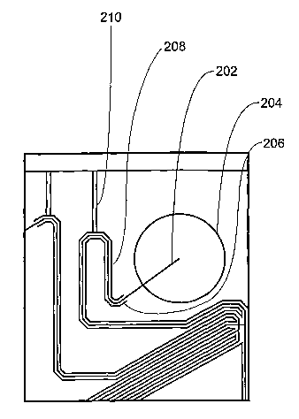
devices. This is further illustrated in Figure 2A, where microfluidic device
body
structure 200 includes venting channel networlcs with venting channels
disposed on two
sides of each microchannel 202. Figure 2B schematically illustrates a
magnified view
of a portion of the body structure depicted in Figure 2A. In this example, a
first venting
channel network includes first venting channel 206 disposed proximal to a
first side of
microchannel 202 in the microchannel network. This embodiment also optionally
12
CA 02410238 2002-11-25
WO 01/97974 PCT/USO1/19595
includes a second venting channel networle in which second venting channel 208
is
disposed proximal to a second side of microchannel 202 of the microchannel
network.
The first and second venting channel networks of microfluidic device
body structure 200 include various alternative formats. For example, as shown
in
Figures 2A and 2B, first and second venting channel (206 and 208,
respectively) of the
first and second venting channel networks are optionally disposed
substantially parallel
to microchannel 202 in the microchannel network. Individual venting channels
of the
first and second venting channel networks optionally include widths of at
least about 5
hum (e.g., 10 ~,m, 50 Vim, 100 ~.m, or more). Additionally, the individual
venting
channels of the first and second venting channel networks typically terminate
at least
about 0.05 mm (e.g., 0.1 mm, 0.3 mm, 0.5, mrn, 1 mm, or more) from an edge of
port
204 when microchannel 202 in the microchannel network fluidly communicates
with
port 204. This prevents fluid flow into the venting channels during operation
of the
device. Although not shown in Figure 2, venting channels optionally fluidly
communicate with ports that are not in fluid communication with microchannel
networks or other device cavities, e.g., to vent bond voids that form during
substrate
bonding. Also, two or more venting channels in the first or second venting
channel
networks typically merge in regions where cross-sectional midpoints of the two
or more
venting channels are separated by at most about 50 ~.m, e.g., to simplify the
fabrication
process. Furthermore, a cross-sectional midpoint of a venting channel is
generally
disposed at least about 60 ~,m from a cross-sectional midpoint of a
microchannel in the
microchannel network. The microchannels typically include a width of at least
about
60 Vim.
As indicated above, in certain embodiments, one or more edges of the
body structure, or a fabrication element (discussed below) which includes a
plurality of
body structures prior to being divided, include a third venting channel
networlc that
includes one or more venting channels, which typically include widths of at
least about
0.1 mm. For example, a venting channel of the third venting channel network
generally
includes a width in the range of from about 0.1 mm to about 3 mm (e.g., 0.2
mm, 0.23
mm, 0.3 mm, 0.35 mm, 0.5 mm, 1 mm, 2 mm, etc.). A venting channel of the third
venting channel network is optionally disposed at least about 3 mm from the
edges of
the body structure. In these embodiments, one or more venting channels of the
venting
channel networks typically fluidly communicate with the third venting channel
network
13 .
CA 02410238 2002-11-25
WO 01/97974 PCT/USO1/19595
to vent bond voids, that form during bonding steps, away from, e.g.,
microchannels or
other functional regions of the device.
In some embodiments of the invention, device body structures are
manufactured with venting cavities disposed therein. Although effective
against bond
voids caused by soft defects (e.g., various types of organic matter), this
form of venting
element is particularly effective against bond voids produced by hard defects,
such as
residual substrate materials (e.g., fiagments of glass, plastic, or the like)
left behind
when microchannel networks or other cavities are fabricated in substrate
surfaces prior
to bonding, as described above:
Figure 3 schematically illustrates one microfluidic device embodiment
that incorporates venting cavities. As shown, plurality of venting cavities
306 is
disposed proximal to two sides of microchannel 302 which intersects with port
304 in
microfluidic device body structure 300. Although depicted as regular shapes,
each
venting cavity is optionally irregularly shaped. Combinations of regular and
irregular
shapes are also possible. For example, two of the three venting cavity
dimensions
together optionally form shapes that include triangles, squares, rectangles,
trapezoids,
regular n-sided polygons, irregular n-sided polygons, circles, ovals, or the
like.
Venting cavities are typically fabricated with volumes of at least about 1
~.m3 (e.g., 50
~.m3, 100 ~,m3, 500 ~,m3, 1000 ~,m3, or more). Additionally, venting cavities
typically
include a depth of at least about 0.1 ~,m (e.g., 1 ~,m, 10 Vim, 100 Vim, or
more). Other
alternatives include spacing each venting cavity at least about 10 hum from
other
venting cavities. Furthermore, venting cavities are optionally regularly or
irregularly
spaced from one another, and at least about 5 ~,m from an edge of a nearest
microchannel, a nearest port, or other functional microfluidic device element.
It will be appreciated that, although venting elements (e.g., venting
channel networlcs, venting cavities, etc.) are optionally fabricated for
communication
with the external environment (e.g., intersections with certain venting
channels of the
third venting channel network, intersections with ports that are not in fluid
communication with other device cavities, or the like), they are also
optionally
fabricated for complete enclosure (i.e., inaccessible to the external
environment) within
bonded components (e.g., fabrication elements, individual body structures, or
the like).
For example, in pre-bonded substrates, venting channel networks are optionally
disposed or positioned in a substrate surface such that they do not or will
not (i.e., upon
14
CA 02410238 2002-11-25
WO 01/97974 PCT/USO1/19595
bonding) intersect with any other component (e.g., other venting channel
networks,
venting cavities, microchannels, ports, or the like) fabricated into the same
surface, or a
different substrate surface to be mated with the substrate surface. Venting
cavities are
similarly also optionally positioned in pre-bonded substrate surfaces. Upon
bonding
(discussed below), venting elements so positioned are completely sealed within
the
bonded structure. This is schematically illustrated by, e.g., plurality of
venting cavities
306 shown in Figure 3.
As a further option, components, such as chambers, cavities, ports, or
the like are fabricated through a substrate such that when the substrate is
bonded to
another substrate, they do not fluidly communicate with any elements (e.g.,
functional
regions) disposed in the other substrate. In Figure 5, this is depicted by,
e.g., non-
functional ports 508. Although not shown in Figure 5, venting elements are
optionally
fabricated to fluidly communicate with such components.
After components such as ports, microchannels, venting elements, arid
the like have been fabricated, first planar surface 110 of top substrate 108
is then
mated, e.g., placed into contact with, and bonded to planar surface 104 of
bottom
substrate 102, covering and sealing the grooves and/or indentations 106 in
planar
surface 104 of bottom substrate 102, to form the channels and/or chambers
(i.e., the
interior portion) of the device at the interface of these two components.
(FIG. 1).
Holes 114 in the top portion of the device are oriented such that they are in
communication with at least one of the channels and/or chambers formed in the
interior
portion of the device from the grooves or indentations in the bottom
substrate. In the
completed device, these holes function as reservoirs for facilitating fluid or
material
introduction into the channels or chambers of the interior portion of the
device, as well
as providing ports at which electrodes may be placed into contact with fluids
within the
device, allowing application of electric fields along the channels of the
device to
control and direct fluid transport within the device.
Optionally, electrodes are disposed relative to the grooves and/or
indentations in the surface of the bottom substrate before the top and bottom
substrates
are mated and bonded. As described further below, these electrode are used,
e.g., to
resistively heat fluidic materials disposed within device cavities. In certain
embodiments, the electrodes or portions thereof are not covered by the top
substrates.
For example, a top substrate is optionally placed adjacent to an electrode
disposed
CA 02410238 2002-11-25
WO 01/97974 PCT/USO1/19595
relative to the grooves and/or indentations in the surface of the bottom
substrate. These
electrodes are generally patterned metal layers of essentially any geometric
shape. For
example, portions of electrodes exposed to fluidic materials in device
cavities typically
include surface areas between about 1 x 10⁻⁶ cm2 and about 100 x 10-4 cm2.
Additionally, at least segments of the electrodes optionally include an outer
layer (e.g.,
platinum, etc.) disposed over an inner layer (e.g., a metal adhesion layer,
such as
titanium, tungsten, an alloy thereof, or the like). Incorporated electrodes
typically
include thicknesses of at most about 0.1 ~m to properly form device cavities
and to
avoid the formation of bond voids upon substrate bonding. Techniques for
fabricating
electrodes suitable for the present invention are generally known.
As mentioned above, multiple microfabricated devices are typically
manufactured at the same time, such as in the form of fabrication elements. To
further
illustrate microfluidic device mass production, Figure 4 depicts fabrication
element
400, which includes multiple microfluidic device body structures. As shown,
each
body structure includes microchannel network 402, individual microchannels of
which
fluidly communicate with certain ports 406 disposed within fabrication element
400.
Additionally, venting channel network 404 is also disposed proximal to at
least portions
of microchannel network 402. Edge or frame channel 408 (e.g., a venting
channel of
the third venting channel network) intersects with venting channel network 404
for
venting bond voids, that form during the substrate bonding step, away from
microchannel networlc 402. As mentioned, fabrication element 400 is optionally
divided to form a plurality of microfluidic device body structures using
techniques
discussed above. Figure 5 shows microfluidic device body structure 500
produced by
severing it from fabrication element 400 depicted in Figure 4. As shown,
microfluidic
device body structure 500 includes microchannel network 502, ports 506, and
venting
channel network 504. In the context of Figure 4 and the above description, the
venting
channel networks protect individual discrete channel networks from bond voids,
whereas frame channels protect multiple discrete channel networks from voids.
However, as described herein, both structures are similar, if not identical in
their basic
structures and functions, e.g., venting channels to block or redirect bond
voids, and can
thus be interchangeably used.
As noted above, the top or second substrate is overlaid upon the bottom
or first substrate to seal the various channels and chambers. In carrying out
the bonding
16
CA 02410238 2002-11-25
WO 01/97974 PCT/USO1/19595
process according to preferred embodiments of the present invention, the
mating of the
first and second substrates is carried out using vacuum to maintain the two
substrate
surfaces in optimal contact, e.g., to minimize the occurrence of bond voids.
However,
as described herein, when bond voids do form, the presence of venting elements
(e.g.,
venting channels, venting cavities, or the like) inhibits them from spreading
into
functionalized regions (e.g., regions having microchannels, etc.) of the
devices. In
particular, the bottom substrate is typically maintained in optimal contact
with the top
substrate by mating the planar surface of the bottom substrate with the planar
surface of
the top substrate, and applying a vacuum through the holes that are disposed
through
the top substrate. In addition, in one set of embodiments, a wicking agent
(e.g., water
or he lilce) is placed between the top and bottom substrate surfaces prior to
application
of the vacuum to assist in establishing optimal contact between the surfaces
to be
bonded. Typically, application of a vacuum to the holes in the top substrate
is carried
out by placing the top substrate on a vacuum chuck, which typically comprises
a
mounting table or surface, having an integrated vacuum source. In the case of
silica-
based substrates, the mated substrates are optionally subjected to elevated
temperatures,
e.g., in the range of from about 100°C to about 200°C, in order
to create an initial bond,
so that the mated substrates may then be transferred to an annealing oven,
without any
shifting relative to each other.
One example of an apparatus for use in accordance with the methods
described herein is shown in Figure 6. As shown, the apparatus includes
mounting
table 600, which includes platform surface 602, having vacuum port 604
disposed
therethrough. In operation, the top substrate (not shown), e.g., having the
plurality of
ports or holes disposed therethrough, is placed upon the platform surface and
maintained in contact with that surface by virtue of the application of a
vacuum through
vacuum port 604. The platform also typically includes one or more alignment
structures (e.g., alignment pins 606, alignment ridges, walls, wells, or the
like) to
ensure alignment of the substrates in the appropriate position, e.g., over
vacuum port
604, as well as aligning the individual substrate portions with other
substrate portions.
In addition to such structures, alignment is also optionally facilitated by
providing the
platform at an appropriate angle, such that gravity will maintain the
substrate in contact
with the alignment structures. Vacuum port 604 is disposed through the
platform
surface and mounting table, and is connected via a vacuum line 608 to a vacuum
source
17
CA 02410238 2002-11-25
WO 01/97974 PCT/USO1/19595
(not shown), e.g., a vacuum pump. For additional details, see, e.g., U.S. Pat.
No.
5,882,465 to McReynolds, above, which is incorporated herein by reference in
its
entirety for all purposes.
Although not shown in Figure 6, the top or second substrate is placed
upon platform surface 602 such that the planar surface of the top substrate
faces away
from platform surface 602 of mounting table 600, and such that the holes or
ports in the
substrate are in communication with vacuum port 604 in platform surface 602 of
mounting table 600. As mentioned, alignment of the holes over vacuum port 604
is
typically accomplished through the incorporation of one or more alignment
structures
upon platform surface 602. In order to apply vacuum simultaneously at a
plurality of
the holes in the top substrate, a series of vacuum ports are optionally
provided through
platform surface 602. Preferably, however, platform surface 602 comprises a
series of
grooves 610 fabricated therein, and extending outward from one vacuum port
604, such
that each of the plurality of holes in the top substrate will be in
communication with
vacuum port 604 via at least one of these "vacuum passages" (i.e., grooves
610) when
the top substrate is placed upon platform surface 602.
The bottom substrate (not shown in Figure 6), also having a first planar
surface, is then placed on the top substrate such that the first planar
surface of the
bottom substrate mates with that of the top substrate. As mentioned, a wicking
agent
(e.g., water or the like) is also optionally placed between the substrate
surfaces to assist
in establishing optimal contact between the surfaces to be bonded. Again, the
alignment structures present upon the platform surface typically operate to
align the
bottom substrate with the top substrate as well as maintain the substrates
over vacuum
port 604. The alignment of the various substrate portions relative to each
other is
particularly important in the manufacture of microfluidic devices, wherein
each
substrate portion typically includes microfabricated elements which are
designed to be
in fluid communication with other microfabricated elements on another
substrate
portion.
A vacuum is then applied through grooves 610 on platform surface 602,
and to the holes through the top substrate. This acts to pull the two
substrates together
by evacuating the air between their planar surfaces. Specifically, upon mating
the top
substrate with the bottom substrate, the holes disposed through the top
substrate will
generally be in communication with the intersecting channel structures
fabricated into
18
CA 02410238 2002-11-25
WO 01/97974 PCT/USO1/19595
the planar surface of the bottom substrate. However, the holes will not
communicate
with venting elements fabricated into the substrates. In these methods, the
channel
networks enhance the efficiency of the bonding process. For example, these
channel
networks typically cover large areas of the surface of the bottom substrate,
or the space
between the two substrates. As such, they typically enhance the efficiency
with which
air, wicking agent, or the lilce are evacuated from this space between the two
substrates,
which is critical to the bonding process. Again, although described in terms
of ports
fabricated in one substrate and channels fabricated in the other, it will be
appreciated
that ports and channels are optionally fabricated in the same substrate andlor
in both
substrates.
In addition to more efficiently removing air, wicking agent, etc. from
between the substrates, the application of vacuum at each of the plurality of
holes in the
top substrate, as well as through the intersecting channel structures between
the two
substrates results in a more even application of the pressure forcing the
substrates
together. Specifically, unevenly applied pressures in bonding methods
typically have
substantial adverse effects on the bonding process. For example, uneven
application of
pressures on the two substrates during the bonding process typically results
in uneven
contact (i.e., bond voids) between the two surfaces of the two substrates,
which, as
described above, reduces the efficiency and quality, as well as the effective
product
yield of the bonding process.
Further, even where substrates are completely bonded under such
uneven pressure, e.g., for thermally bonded polymeric substrates or substrates
bonded
with adhesives, such uneven pressures typically result in variations in the
dimensions of
the internal structures of the device from one location in a microfabricated
device to
another. Again, the channel networks extending across wide areas of the
interior
portion of the two substrates, e.g., fabricated into the surface of the second
substrate,
allows application of vacuum across a substantially larger, and more evenly
distributed
area of the interior portion of the substrates. Furthermore, although not
directly
affected by the application of vacuum, venting elements, as discussed, serve
to prevent
bond voids that do form from impacting the channel networks.
In addition to a vacuum chuck, bonding systems also optionally include
a heat source, e.g., a controllable heat source such as a heat gun, for
elevating the
temperature of the top and bottom substrates while they are mounted on the
platform
19
CA 02410238 2002-11-25
WO 01/97974 PCT/USO1/19595
surface/mounting table. For bonding silica-based substrates, this optional
heat source
applies an elevated temperature to the two substrates to create a preliminary
bond
between the substrates, so that they may be readily transferred to an
annealing oven
without the substrates shifting substantially relative to each other. This is
generally
accomplished by heating the two substrates to between about 90°C and
about 200°C. In
the case of polymeric substrates, this heat source typically takes the place
of the
annealing oven by elevating the temperature of the polymeric substrates to
appropriate
bonding temperatures, e.g., between about 80°C and 200°C.
Further, this is optionally
done while the substrates are mounted upon the mounting table, and while a
vacuum is
being applied to the substrates. As mentioned, this has the effect of
maintaining an
even, constant pressure on the substrates throughout the bonding process.
Following
such initial bonding, the substrates are transferred to an annealing oven,
e.g., as
described above, where they are subjected to bonding temperatures between
about
500°C and 1400°C, again, as described above.
It will be readily appreciated that the heat source portion of the
apparatus optionally includes multiple heat sources, i.e., heat guns, or
optionally
includes heating elements integrated into the apparatus itself. For example, a
thermoelectric heater is optionally fabricated into or placed in thermal
contact with the
platform surface/mounting table, which itself, is optionally fabricated from a
thermally
conductive material. Such thermal bonding systems are equally applicable to
both
polymeric substrates and silica-based substrates, e.g., for overall bonding of
polymeric
substrates, or for producing the initial, preliminary bonding of the silica-
based
substrates.
Alternate bonding systems for incorporation with the apparatus
described herein include, e.g., adhesive dispensing systems, for applying
adhesive
layers between the two planar surfaces of the substrates. This is optionally
done by
applying the adhesive layer prior to mating the substrates, or by placing an
amount of
the adhesive at one edge of the adjoining substrates, and allowing the wiclung
action of
the two mated substrates to draw the adhesive across the space between the two
substrates.
In certain embodiments, the overall bonding system optionally includes
automatable systems for placing the top and bottom substrates on the mounting
surface
and aligning them for subsequent bonding. Typically, such systems include
translation
CA 02410238 2002-11-25
WO 01/97974 PCT/USO1/19595
systems for moving either the mounting surface or one or more of the top and
bottom
substrates relative to each other. For example, robotic systems are optionally
used to
lift, translate and place each of the top and bottom substrates upon the
mounting table,
and within the alignment structures, in turn. Following the bonding process,
such
systems also optionally remove the finished product from the mounting surface
and
transfer these mated substrates to a subsequent operation, e.g., separation
operation,
annealing oven for silica-based substrates, etc., prior to placing additional
substrates
thereon for bonding.
Many applications performed in or by the devices of the present
invention are temperature dependent. In the context of microfluidics, for
example, one
temperature control technique entails resistively or Joule heating fluidic
materials
within microfluidic devices by flowing current through electrodes or other
conductive
components positioned, e.g., within a microchannel or other device cavity. The
resulting flow of current into fluid within the cavities of a device
resistively heats the
fluid by dissipating energy through the electrical resistance of the fluid.
Specific microfluidic applications that involve resistive heating include
nucleic acid amplification methods, such as the widely-known polymerase chain
reaction (PCR). The PCR typically includes repeated thermocycles that denature
double-stranded target nucleic acids, hybridize single-stranded target and
primer
nucleic acids, and elongate primer strands with a polymerase. Many variations
of this
basic technique are also known, including asymmetric PCRs, assembly PCRs,
reverse
transcription PCRs (RT-PCRs), ligase chain reactions (LCRs), or the like.
Amplification methods, such as these, are described further in, e.g., F.M.
Ausubel et al.,
eds., Current Protocols in Molecular Biolo~y, Current Protocols, a joint
venture
between Greene Publishing Associates, Inc. and John Wiley & Sons, Inc.
(supplemented through 2000), Sambrook et al., Molecular Cloning - A Laboratory
Manual (2nd Ed.), Vol. 1-3, Cold Spring Harbor Laboratory, Cold Spring Harbor,
New
Yorlc (1989), Newton and Graham, PCR (2nd Ed.), Scientific Publishers, Oxford,
England (1997), Herrington and O'Leary, eds., PCR 3: In Situ Hybridization,
IRL Press
at Oxford University Press, Inc., Oxford, England (1997), Smeltzer, ed., PCR
In
Bioanal~: Methods in Molecular Biolo~y, Vol. 92, Humana Press, Towata, N.J.
(1998), and Innis et al., eds., PCR Strategies, Academic Press, San Diego, CA
(1995).
21
CA 02410238 2002-11-25
WO 01/97974 PCT/USO1/19595
Nucleic acid sequencing or genotyping techniques, such as the Sanger
dideoxy method, which is generally known in the art, are also optionally
performed
using the microfluidic devices arid methods of providing resistive heat in the
present
invention. The dideoxy method typically includes performing repeated
thermocycles to
extend primers hybridized to single-stranded target nucleic acids with a
polymerase
(e.g., Taq DNA polymerase) in reaction mixtures that also include the four
dNTPs, and
one of the four dideoxy analogues (e.g., a 2',3'-dideoxy analog), which
terminates the
extension reaction upon incorporation. Sequences are typically determined by
detecting signals, e.g., from radioactive or fluorescent labels incorporated
into the
extended primer strands. Sequencing formats, including cycle sequencing are
described in a variety of references, including, e.g., Rapley, PCR Sequencing
Protocols,
Humana Press, Towata, N.J. (1996), Griffin and Griffin, Eds., DNA Seguencing
Protocols, Humana Press, Towata, N.J. (1993), Roe et al., DNA Isolation and
Sectuencin~, John Wiley & Sons, New York, N.Y. (1996), Adams et al., Eds.,
Automated DNA Seduencin~ and Analysis, Academic Press, San Diego, CA (1994),
and Alphey, DNA Sequencing from Experimental Methods to Bioinformatics,
Springer
Verlag, New York, N.Y. (1997). See also, Maxam and Gilbert (1977) "A New
Method
for Sequencing DNA," Proc. Natl. Acad. Sci. U.S.A. 74:560-564 and Sanger et
al.
(1977) "DNA Sequencing with Chain-Terminating Inhibitors," Proc. Natl. Acad.
Sci.
U.S.A. 74:5463-5467. Applications of sequencing and other techniques in
microfluidic
systems are found in, e.g., published PCT applications WO 98/45481, WO
00/50172,
and WO 00/50642.
Although, nucleic acid amplification and sequencing are discussed
above for purposes of illustration, it will be appreciated that the
resistively heating
microfluidic cavities is optionally used for essentially any other application
or assay in
which temperature control is desired.
To increase throughput, multiple reactions are optionally performed
simultaneously in parallel reaction channels of a particular device. In these
applications, it is typically desirable to achieve temperature uniformity
across the
multiple heated channels and also to reduce the power requirements to maintain
temperatures within the device above the ambient temperature. In microfluidic
devices
that lack venting elements, there may be significant amounts of heat lost to
the
substrate material, which results in temperature distributions between
channels. This is
22
CA 02410238 2002-11-25
WO 01/97974 PCT/USO1/19595
illustrated in Figure 7, which provides a data graph that shows the results of
steady
resistive heating simulations performed in a device modeled to include nine
parallel
channels. Neighboring channels of the modeled device were separated by 250 ~m
from
one another. The modeled device also included a 22C isothermal lower surface
or
bottom and the applied voltage was 2000V. Temperature (°C) is indicated
on the
abscissa, while the particular channel number is provided on the ordinate.
Average
temperature 700 was between about 106°C and 107°C. As shown,
individual channel
temperatures 702 varied by as much as about 25°C in the simulations.
Such
temperature variation would be unacceptable, e.g., for PCR applications since
tight
temperature control is generally necessary in order to maintain reaction
specificity.
The largest temperature variations are typically projected at the
outermost channels of a given device, as they lack channels adjacent to their
outer
edges with which to couple, and as a consequence, dissipate heat into larger
regions of
open substrate, e.g., portions of the substrate lacking channels disposed
therein. In
preferred aspects, the invention provides insulating venting elements, such as
voids,
cavities, channels, or the lilce disposed proximal to at least these outermost
channel
edges, thereby gaining substantial uniformity of temperature over the full
range of
channels. As used herein, "substantial uniformity" refers to temperatures that
vary by,
e.g., less than about 30%, less than about 20%, less than about 10%, or less
than about
5%, or less from one channel to any other channel in a particular device. For
example,
substantially uniform temperatures typically vary by, e.g., less than about
10°C, less
than about 5°C, less than about 2°C, or less. In certain
aspects, insulating venting
elements may be provided only at these outermost edges and not between the
heated
channels, so as to allow the various heated channels to be thermally coupled,
thereby
potentially reducing the energy requirements of the system.
In the present invention, venting elements are optionally fabricated to
provide discontinuous changes in the thermal conductivity of the particular
substrate
material to reduce the lateral flow of heat. In particular, a venting element
forms an air-
gap that provides a significant barner to heat transfer between regions in the
device.
For example, an air gap will thermally insulate and reduce thermal coupling
between
two heated channels. This is illustrated in Figure 8A, which schematically
depicts a top
view of microfluidic device 800. As shown, microfluidic device 800 includes
parallel
23
CA 02410238 2002-11-25
WO 01/97974 PCT/USO1/19595
channels 802, each of which fluidly communicates with two ports 804. As also
shown,
parallel channels 802, each include venting elements 806 disposed to either
side to
reduce the thermal coupling between parallel channels 802, which permits,
e.g.,
independent temperature control of each channel 802. As depicted, venting
elements
806 are disposed completely through microfluidic device 800. Figure 8B
schematically
illustrates a cross-sectional view of microfluidic device 800. Although not
shown,
venting elements 806 are optionally disposed only partially through or
completely
within microfluidic device 800. Optionally, venting elements are used to
thermally
insulate multiple cavities or channels in a selected region or zone of a
device, e.g., to
maintain the cavities in the selected region at a selected temperature and to
reduce
thermal interference with other zones.
In certain aspects, it is preferred that the venting elements are disposed
partially through the microfluidic device. In particular, it is often
desirable to fabricate
venting elements, e.g., thermal insulating elements or void venting elements
using the
same processes used to fabricate the channels within the microfluidic device,
e.g.,
photolithography/wet chemical etching, injection molding, embossing, e'tc. As
such,
the various non-channel venting elements will appear very similar to the
operative
channels of the device (e.g., fluid conduits). In certain aspects, better
thermal
insulation may be achieved by providing such insulating channels deeper than
the fluid
channels of the device to provide optimal thermal insulation, or as provided
above,
providing such elements disposed entirely through at least one of the
substrates of the
device.
In certain embodiments, for example, the venting element is disposed in
the body structure and produces a stagnant vapor region that reduces
convective
transport between venting element surfaces. In embodiments where the venting
element is disposed at least partially through the body structure, at least
one surface of
the body structure optionally further includes at least one substrate disposed
over (e.g.,
bonded as described above) at least a segment of the venting element to
produce a
stagnant vapor region that reduces convective transport between venting
element
surfaces.
In addition to the temperature control advantages provided by insulating
different portions of a given device from one another, the total amount of
power used to
heat a channel is reduced, because less of the device is heated to maintain a
selected
24
CA 02410238 2002-11-25
WO 01/97974 PCT/USO1/19595
temperature. Furthermore, venting elements also enhance heat removal in the
vertical
direction. Optionally, an active cooling element, such as a cooling fan, a
cooled heat
sink, a pettier cooler, or the like, is used to further enhance the vertical
removal of heat
from the device.
Although the methods and devices of the present invention are
optionally applied to any process in which specific substrate regions are to
be protected
from the impact of bond voids, in preferred embodiments, the invention relates
to the
fabrication of microfluidic devices. As a result, this disclosure emphasizes
the
microfluidic applications of the present invention.
As used herein, the term "microscale" or "microfabricated" generally
refers to structural elements or features of a device which have at least one
fabricated
dimension in the range of from about 0.1 ~.m to about 500 hum. Thus, a device
referred
to as being microfabricated or microscale will include at least one structural
element or
feature having such a dimension. When used to describe a fluidic element, such
as a
channel, passage, chamber or conduit, the terms "microscale,"
"microfabricated" or
"microfluidic" generally refer to one or more fluid channels, passages,
chambers or
conduits which have at least one internal cross-sectional dimension, e.g.,
depth, width,
length, diameter, etc., that is less than 500 ~,m, and typically between about
0.1 ~m and
about 500 ~,m.
In the devices of the present invention, the microscale channels or
chambers preferably have at least one cross-sectional dimension between about
0.1 ~,m
and 200 Vim, more preferably between about 0.1 ~.m and 100 [gym, and often
between
about 0.1 ~m and 50 p,m. Accordingly, the microfluidic devices or systems
prepared in
accordance with the present invention typically include at least one
microscale channel,
usually at least two intersecting microscale channels, and often, three or
more
intersecting channels disposed within a single body structure. Channel
intersections
optionally exist in a number of formats, including cross intersections, "Y"
andlor "T"
intersections, or any number of other structures whereby two channels are in
fluid
communication.
The manufacture of many different microscale systems is optionally
adapted in accordance with the methods and devices of the present invention
by, e.g.,
incorporating venting cavities, venting channels, frame channels, or the like,
into pre-
CA 02410238 2002-11-25
WO 01/97974 PCT/USO1/19595
assembled substrate surfaces, as discussed below. These systems are described
in
numerous publications by the inventors and their coworkers. These include
certain
issued U.S. Patents, including U.S. Patent Nos. 5,699,157 (J. Wallace Parce)
issued
12/16/97, 5,779,868 (J. Wallace Parce et al.) issued 07/14/98, 5,800,690
(Calvin Y.H.
Chow et al.) issued 09/01/98, 5,842,787 (Anne R. Kopf-Sill et al.) issued
12/01/98,
5,852,495 (J. Wallace Parce) issued 12/22/98, 5,869,004 (J. Wallace Parce et
al.) issued
02/09/99, 5,876,675 (Colin B. Kennedy) issued 03/02/99, 5,880,071 (J. Wallace
Parce
et al.) issued 03/09/99, 5,882,465 (Richard J. McReynolds) issued 03/16/99,
5,885,470
( J. Wallace Parce et al.) issued 03/23/99, 5,942,443 (J. Wallace Parce et
al.) issued
08/24/99, 5,948,227 (Robert S. Dubrow) issued 09/07/99, 5,955,028 (Calvin Y.H.
Chow) issued 09/21/99, 5,957,579 (Anne R. Kopf-Sill et al.) issued 09/28/99,
5,958,203 (J. Wallace Parce et al.) issued 09/28/99, 5,958,694 (Theo T.
Nilciforov)
issued 09/28/99, 5,959,291 (Morten J. Jensen) issued 09/28/99, 5,964,995 (Theo
T.
Nikiforov et al.) issued 10/12/99, 5,965,001 (Calvin Y. H. Chow et al.) issued
10/12/99,
5,965,410 (Calvin Y. H. Chow et al.) issued 10/12/99, 5,972,187 (J. Wallace
Parce et
al.) issued 10/26/99, 5,976,336 (Robert S. Dubrow et al.) issued 11/2/99,
5,989,402
(Calvin Y. H. Chow et al.) issued 11/23/99, 6,001,231 (Anne R. Kopf-Sill)
issued
12114/99, 6,011,252 (Morten J. Jensen) issued 1/4/00, 6,012,902 (J. Wallace
Parce)
issued 1/11/00, 6,042,709 (J. Wallace Parce et al.) issued 3/28/00, 6,042,710
(Robert S.
Dubrow) issued 3/28/00, 6,046,056 (J. Wallace Parce et al.) issued 4/4/00,
6,048,498
(Colin B. Kennedy) issued 4/11/00, 6,068,752 (Robert S. Dubrow et al.) issued
5/30/00,
6,071,478 (Calvin Y. H. Chow) issued 6/6/00, 6,074,725 (Colin B. Kennedy)
issued
6/13/00, 6,080,295 (J. Wallace Parce et al.) issued 6/27/00, 6,086,740 (Colin
B.
Kennedy) issued 7/11/00, 6,086,825 (Steven A. Sundberg et al.) issued 7/11/00,
6,090,251 (Steven A. Sundberg et al.) issued 7/18/00, 6,100,541 (Robert Nagle
et al.)
issued 8/8/00, 6,107,044 (Theo T. Niluforov) issued 8/22/00, 6,123,798
(Khushroo
Gandhi et al.) issued 9/26100, 6,129,826 (Theo T. Nikiforov et al.) issued
10/10/00,
6,132,685 (Joseph E. Kersco et al.) issued 10/17/00, 6,148,508 (Jeffrey A.
Wolk) issued
11/21/00, 6,149,787 (Andrea W. Chow et al.) issued 11/21/00, 6,149,870 (J.
Wallace
Parce et al.) issued 11/21/00, 6,150,119 (Anne R. Kopf-Sill et al.) issued
11/21/00,
6,150,180 (J. Wallace Parce et al.) issued 11/21/00, 6,153,073 (Robert S.
Dubrow et al.)
issued 11/28/00, 6,156,181 (J. Wallace Parce et al.) issued 12/5/00, 6,167,910
(Calvin
Y. H. Chow) issued 1/2/01, 6,171,067 (J. Wallace Parce) issued 1/9/01,
6,171,850
26
CA 02410238 2002-11-25
WO 01/97974 PCT/USO1/19595
(Robert Nagle et al.) issued 1/9/01, 6,172,353 (Morten J. Jensen) issued
1/9/01,
6,174,675 (Calvin Y. H. Chow et al.) issued 1/16/01, 6,182,733 (Richard J.
McReynolds) issued 2/6/01, 6,186,660 (Anne R. Kopf-Sill et al.) issued
2/13/01,
6,221,226 (Anne R. Kopf-Sill) issued April 24, 2001, 6,233,048 (J. Wallace
Parce)
issued 5/15/01, 6,235,175 (Robert S. Dubrow et al.) issued 5122/01, 6,235,471
(Michael
Knapp et al.) issued 5/22/01, and 6,238,538 (J. Wallace Parce et al.) issued
5/29/01.
These systems are also described in various PCT applications by the
inventors including, e.g., WO 98/00231, WO 98/00705, WO 98/00707, WO 98/02728,
WO 98/05424, WO 98/22811, WO 98/45481, WO 98/45929, WO 98146438, and WO
98/49548, WO 98/55852, WO 98/56505, WO 98/56956, WO 99/00649, WO 99/10735,
WO 99/12016, WO 99/16162, WO 99/19056, WO 99/19516, WO 99/29497, WO
99/31495, WO 99/34205, WO 99/43432, WO 99/44217, WO 99/56954, WO 99/64836,
WO 99/64840, WO 99/64848, WO 99/67639, WO 00/07026, WO 00/09753, WO
00/10015, WO 00/21666, WO 00/22424, WO 00/26657, WO 00/42212, WO 00/43766,
WO 00/45172, WO 00/46594, WO 00/50172, WO 00/50642, WO 00/58719, WO
00/60108, WO 00/70080, WO 00/70353, WO 00/72016, WO 00/73799, WO 00/78454,
WO 01/02850, WO 01/14865, WO 01/17797, and WO 01/27253.
While the foregoing invention has been described in some detail for
purposes of clarity and understanding, it will be clear to one spilled in the
art from a
reading of this disclosure that various changes in form and detail can be made
without
departing from the true scope of the invention. For example, all the
techniques and
apparatus described above may be used in various combinations. All
publications,
patents, patent applications, or other documents cited in this application are
incorporated by reference in their entirety for all purposes to the same
extent as if each
individual publication, patent, patent application, or other document were
individually
indicated to be incorporated by reference for all purposes.
27