Language selection

Search

Patent 2411127 Summary

Third-party information liability

Some of the information on this Web page has been provided by external sources. The Government of Canada is not responsible for the accuracy, reliability or currency of the information supplied by external sources. Users wishing to rely upon this information should consult directly with the source of the information. Content provided by external sources is not subject to official languages, privacy and accessibility requirements.

Claims and Abstract availability

Any discrepancies in the text and image of the Claims and Abstract are due to differing posting times. Text of the Claims and Abstract are posted:

  • At the time the application is open to public inspection;
  • At the time of issue of the patent (grant).
(12) Patent: (11) CA 2411127
(54) English Title: SIGNAL LAMPS AND APPARATUS
(54) French Title: LAMPES ET APPAREILS DE SIGNALISATION
Status: Expired and beyond the Period of Reversal
Bibliographic Data
(51) International Patent Classification (IPC):
  • H05B 45/52 (2020.01)
  • B61L 5/18 (2006.01)
(72) Inventors :
  • TICHBORNE, FRANK GEORGE (United Kingdom)
  • BURTON, COLIN (United Kingdom)
(73) Owners :
  • SIEMENS RAIL AUTOMATION HOLDINGS LIMITED
(71) Applicants :
  • SIEMENS RAIL AUTOMATION HOLDINGS LIMITED (United Kingdom)
(74) Agent: SMART & BIGGAR LP
(74) Associate agent:
(45) Issued: 2014-08-19
(22) Filed Date: 2002-11-05
(41) Open to Public Inspection: 2003-06-11
Examination requested: 2007-04-13
Availability of licence: N/A
Dedicated to the Public: N/A
(25) Language of filing: English

Patent Cooperation Treaty (PCT): No

(30) Application Priority Data:
Application No. Country/Territory Date
0129610.2 (United Kingdom) 2001-12-11

Abstracts

English Abstract

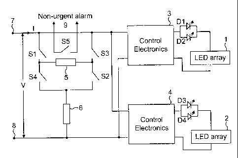
An LED signal lamp comprises at least two separate LED arrays which have separate power feeds and wherein the LEDs of the arrays are positioned with respect to each other such that when lit they provide a composite light signal output and such that when the LEDs of only one of the two arrays are lit they provide a light signal with a visible distinctive pattern. A distinctive pattern is revealed, either lit or dark. Typically this pattern may be formed as a letter such as "X" or "F" or may be foamed as a striped effect, for example. An LED signal apparatus comprises input signal power supply terminals 7,8 for the apparatus; a series connection of switch means S1 to S4 and a ballast load 6 connected across the supply terminals 7,8; an LED signal lamp 1,2 connected to the terminals to be supplied with current therefrom; and switch operating means D1 to D4, in the supply path to the LED lamp, for controlling the state of the switch means S1 to S4 in the series connection, whereby total failure or substantially total failure of the current to the LED signal lamp results in said switch operating means D1 to D4 causing said switch means to open to disconnect the ballast load 6 from power from the supply terminals 7,8.


French Abstract

Une lampe à signal à diodes électroluminescentes (DEL) comprend au moins deux réseaux de DEL possédant des alimentations distinctes et dont les DEL sont positionnées les unes par rapport aux autres de manière que, lorsqu'elles sont allumées, elles fournissent une sortie de signal de lumière composite et de façon que, lorsque les DEL de seulement un des deux réseaux sont allumées, elles fournissent un signal de lumière présentant un motif distinctif visible. Un motif distinctif lumineux ou sombre apparaît. Généralement, ce motif peut former une lettre, comme « X » ou « F », ou un effet à bandes, par exemple. Un appareil à signal à DEL comprend des bornes d'alimentation de signal d'entrée (7,8) pour l'appareil; une connexion en série de moyens de commutation S1 à S4 et une charge de délestage (6) connectée aux bornes d'alimentation (7,8); une lampe à signal à DEL (1,2) connectée aux bornes à alimenter par du courant à partir de ces dernières; et des moyens de commutation D1 à D4, dans la voie d'alimentation de la lampe à DEL, pour commander l'état des moyens de commutation S1 à S4 dans la connexion en série, la coupure totale ou quasi totale du courant à la lampe à signal à DEL faisant en sorte que ledit commutateur active les moyens de commutation D1 à D4, ce qui entraîne l'ouverture desdits moyens de commutation pour déconnecter la charge de délestage (6) du courant provenant des bornes d'alimentation (7,8).

Claims

Note: Claims are shown in the official language in which they were submitted.


8
Claims:
1. An LED signal lamp comprising at least two separate LED arrays which are
connected in parallel such that they have separate power feeds and circuitry
connected with
the LED arrays and wherein the LEDs of the arrays are positioned with respect
to each other
such that when lit they provide a composite light signal output and such that
should the
current through either array fail, the LEDs of the other array may still
light, and when the
LEDs of only one of the two arrays are lit the lamp provides a signal with a
visible distinctive
pattern to provide a first indication of a failure of an array, said circuitry
providing an alarm
as a second indication of said failure.
2. An LED signal lamp according to claim 1 wherein the distinctive pattern
is revealed,
either lit or dark.
3. An LED signal lamp according to claim 2 wherein the pattern is formed as
an
alphabetic letter or as a striped effect.
4. An LED signal lamp comprising at least two separate LED arrays which
have
separate power feeds and a switchable routing arrangement such that current
may flow along
different routes through the routing arrangement in dependence of a switching
state of the
routing arrangement, and wherein the LEDs of the arrays are positioned with
respect to each
other such that when lit they provide a composite light signal output and such
that should the
current through either array fail, the LEDs of the other array may still
light, and when the
LEDs of only one of the two arrays are lit the lamp provides a signal with a
visible distinctive
pattern providing a first indication of the failure of an array and the
switchable routing
arrangement is switched to provide an alarm as a second indication of the
failure of said
array.
5. An LED signal lamp according to claim 4, wherein the switchable routing
arrangement comprises a plurality of switches.
6. An LED signal lamp according to claim 5, wherein the LEDs of only one of
the two

9
arrays are lit, the routing arrangement is switched to enable current to flow
through a
particular route, thus activating the alarm.
7. An LED
signal lamp according to claim 6, wherein the switches are controlled by
respective switch operating means responsive to the flow of current though an
LED array.

Description

Note: Descriptions are shown in the official language in which they were submitted.


CA 02411127 2002-11-05
"
1
Signal Lamps and Apparatus
The present invention relates to signal lamps and apparatus and particularly,
although not exclusively, to railway signal lamps and apparatus and
particularly to lamps
and apparatus utilising Light Emitting Diodes (LEDs) as light emitters instead
of normal
filament bulbs.
An LED signal consist of a multiplicity of LEDs which collectively produce a
monochromatic light emitting from a viewing aperture equivalent in size to a
conventional
filament lamp light signal aperture. Since the source is not a single filament
as in a bulb,
the LEDs are arranged in a pattern of points over the aperture. Use of LEDs
has the
advantage over single filament bulbs that, whilst individual LEDs may fail,
this does not
cause complete failure of the signal lamp as occurs with a bulb single
filament failure. A
failure in the control supply to the LEDs would, however, cause a complete
failure.
According to one aspect of the present invention an LED signal lamp comprises
at
least two separate LED arrays which have separate power feeds and wherein the
LEDs of
the arrays are positioned with respect to each other such that when lit they
provide a
composite light signal output and such that when the LEDs of only one of the
two arrays
are lit they provide a light signal with a visible distinctive pattern.
According to one embodiment of the invention an LED signal lamp is formed with
two LED arrays, each forming half of the signal display and each having
separate control
electronics supplied from the signalling supply. Hence if either half fails,
either in the
electronics or =some of the LEDs such that current ceases to flow in the
array, then half of
the LEDs extinguish. The LEDs of the two arrays are arranged such that, on
extinguishing
of one array with the remaining half of the LEDs formed by the other array
remaining =
alight, a distinctive pattern is revealed, either lit or dark. Typically this
pattern may be
formed as a letter such as "X" or "F" or may be formed as a striped effect,
for example. A
viewer (typically a train driver) of a signal in this state will interpret the
displayed signal

CA 02411127 2002-11-05
2
as a valid signal, but a signal that has to be reported as defective in
appearance, resulting
in a maintenance alert where the defective aspect of the signal can be
replaced.
An LED signal lamp typically takes less power (6 Watts) than an equivalent
filament lamp type signal(30 Watts). Hence when replacing Filament lamp
signals with
LED signal lamps in the existing railway signalling, the LED signal current
needs to be
ballasted to equate with that of a Filament lamp when lit, to enable the
existing signal
interlocking circuitry to detect a dark signal failure. The ballasting is
effected utilising a
ballast resistor in parallel with the LED signal across the signal supply.
With the typical
levels of power consumption mentioned above, this ballast resistor will take
approximately
80% of the supplied current.
In the existing railway signalling network, it is substantial cessation of
supply
current during a signal operation phase that indicates signal failure. It is,
therefore,
imperative that some form of interlock be applied to ensure that, if LED
current stops, the
ballast load is also disconnected from the supply. This has typically been
performed by a
fuse blow circuit. However because of the active nature of this circuit, it is
inherently less
reliable than the dropped relay version as applied to a filament lamp which is
inherently
fail safe.
According to a second aspect of the present invention, an LED signal apparatus
comprises input signal power supply terminals for the apparatus; a series
connection of
switch means and a ballast load connected across the supply terminals; an LED
signal lamp
connected to the terminals to be supplied with current therefrom; and switch
operating
means, in the supply path to the LED lamp, for controlling the state of the
switch means in
the series connection, whereby, during operation of the apparatus, total
failure or
substantially total failure of the current to the LED signal lamp results in
said switch
operating means causing said switch means to open to disconnect the ballast
load from
power from the supply terminals.

CA 02411127 2014-02-25
54106-1457
3
Advantageously, the switch operating means may comprise an optocoupled
diode for controlling an electronic switch such that, if electric current
flows through the diode,
the electronic switch closes and vice versa.
In preferred embodiments of the invention, the LED signal lamp comprises at
least two separate LED arrays arranged jointly to provide a signal light
output for the lamp
and wherein each of said arrays has an individual switch control means in its
supply path and
said ballast load is connected to said supply terminals through a plurality of
switch means
each controlled by a respective one of the switch control means and the
arrangement is such
that provided current flows to one of said arrays, the corresponding switch
control means
controls its respective switch means to permit current to flow through the
ballast load.
Preferably, in such an arrangement, detection means are provided to detect
that not all the
switch means are a permitting flow of current to the ballast load and to
provide a non-urgent
alarm signal to that effect. Such an alarm signal would normally indicate
failure of current
flow through the array associated with the corresponding switch control means.
The detection
means may comprise a relay with its relay coil connected between switch means
controlled
points, in the supply to the ballast load, that are at substantially the same
voltage during
closure a of all switch means but which are at different voltages, in the
event of opening of
only one of the switch means, such that relay operating current flows through
the relay coil.
Preferably, a pair of switch control means are connected in parallel in the
supply to an array such that supply of current to the array is not interrupted
solely as the result
of failure of a single switch control means. Additionally there may be a pair
of switch means
each associated with a respective one of the pair of switch control means.
According to one aspect of the present invention, there is provided an LED
signal lamp comprising at least two separate LED arrays which are connected in
parallel such
that they have separate power feeds and circuitry connected with the LED
arrays and wherein
the LEDs of the arrays are positioned with respect to each other such that
when lit they

CA 02411127 2014-02-25
54106-1457
3a
provide a composite light signal output and such that should the current
through either array
fail, the LEDs of the other array may still light, and when the LEDs of only
one of the two
arrays are lit the lamp provides a signal with a visible distinctive pattern
to provide a first
indication of a failure of an array, said circuitry providing an alarm as a
second indication of
said failure.
According to another aspect of the present invention, there is provided an LED
signal lamp comprising at least two separate LED arrays which have separate
power feeds and
a switchable routing arrangement such that current may flow along different
routes through
the routing arrangement in dependence of a switching state of the routing
arrangement, and
wherein the LEDs of the arrays are positioned with respect to each other such
that when lit
they provide a composite light signal output and such that should the current
through either
array fail, the LEDs of the other array may still light, and when the LEDs of
only one of the
two arrays are lit the lamp provides a signal with a visible distinctive
pattern providing a first
indication of a failure of an array and the switchable routing arrangment is
switched to
provide an alarm as a second indication of the failure of said array.
For a better understanding of the present invention, reference will now be
made
to the accompanying drawings, in which, solely by way of example:
Figure 1, shows diagrammatically the circuit of one embodiment of railway
signal lamp apparatus in accordance with the second aspect of the invention;
and

CA 02411127 2002-11-05
4
Figure 2, shows diagrammatically the circuit of a second embodiment of railway
signal lamp apparatus in accordance with the second aspect of the invention.
In both figures, the same references have been used for the same or
corresponding
elements.
The circuit arrangement of Fig.1 has two LED arrays 1 and 2, housed together
in
the same lamp (not shown) and designed to provide together the output signal
light for the
lamp. LED array 1 is connected to an array control electronics unit 3 through
two supply
lines, in one of which there are two optocoupled diodes D1 and D2. Similarly,
LED array
2 is coupled to control electronics unit 4 through two separate supply lines,
of which one
includes parallel connected optocoupled diodes D3 and D4.
Two signal power terminals for the apparatus are referenced 7 and 8 and the
signal
supply voltage and current are shown as V and 1 respectively. These supply
terininals are
connected directly, to supply signal power thereto, to the control electronics
units 3 and 4.
A ballast load 6 is connected across terminals 7 and 8, one end being
connected directly to
terminal 8 with the other end being connected to terminal 7 through two pairs
of switches
S1, S4 and S3, S2. The switches of each pair of switches are connected in
series between
terminal 7 and said other end of the ballast load 6. The junction between the
switches of
each pair of switches are connected via the coil of a relay 5. Switch contacts
S5 of relay 5
are coupled to a "non-urgent alarm" output 9. The switching state of each of
the switches
S1 to S4 is controlled by the correspondingly numbered optocoupled diodes D1
to D4. =
As indicated, the LED signal lamp is formed with two LED arrays 1 and 2, each
forming half of the signal display.and each having separate control
electronics supplied
fiom the signalling supply. Hence, if either half fails, either in the
electronics or in the LED
array such that current ceases to flow in the array, then half of the LEDs
extinguish. The
LEDs of the two arrays are arranged such that, on extinguishing of one array
with the
remaining half of the LEDs formed by the other array remaining alight, a
distinctive pattern

CA 02411127 2002-11-05
is revealed, either lit or dark. Typically this pattern may be formed as a
letter such as "X"
or "F" or may be formed as a striped effect, for example. As a result, a
viewer (typically a
train driver) of a signal in this state will interpret the displayed signal as
a valid signal but
one that has to be reported as defective in appearance, resulting in a non-
urgent
5 maintenance alert where the defective aspect of the signal can be replaced.
In the Fig.1 circuit, when power is applied to the input terminals 7,8, both
control
electronics units 3and 4 provide independent power to LED arrays 1 and 2 via
the diodes
D1 and D2 (for LED array-1) and D3 and D4 (for LED array-2). These four
optocoupled
diodes, control switches SI, S2, S3 and S4 respectively such that if current
flows through
DI electronic switch S1 closes. Normally, on application of signal power,
current flows
through all 4 diodes D1-D4 and hence Sl-S4 are closed. This results in the
ballast load 6
being in circuit, connected across the power supply terminals 7 and 8, and the
combined
effect of the ballast load 6 and the LED current, via the 2 sets of control
electronics are
arranged to be equivalent in load to that of a normal filament signal lamp.
Hence, the
normal hot filament proving circuit, in the standard existing control signal
interlocking
arrangement, will detect what it believes to be a normally operating filament
signal lamp
and react conectly. In this normal condition the voltage across the coil of
the non-urgent
alarm relay 5 is effectively zero and hence the contact S5 (which is normally
closed)
remains closed.
In the case where current stops flowing through one or other LED array
(causing it
not to be lit), then two switches will open. For example if LED array 1 fails,
then S1 and
S2 open and current then flows via S3, the relay coil and S4 to the ballast
load 6. Similarly
if LED array 2 fails then S3 and S4 open and current then flows via Sl, the
relay coil 5 and
S2 to the ballast load 6. Hence in either of these partial failure cases, the
non-urgent alarm
output 9 is signalled by the opening of contact S5. However the signal load
cuiTent,
although reduced slightly, is still sufficient to indicate to the interlocking
control that the
lamp is operational. This is equivalent to the first filament failure alarm in
a conventional
signal.

CA 02411127 2002-11-05
,
6
In the very rare event that current stops being supplied to both LED arrays,
then all
4 switches SI to S4 open and the ballast load is removed from circuit. This
effect, plus the
loss of current to both arrays results in a loss of load current from the
interlocking control
arrangement sufficiently to guarantee the asserting of an Urgent Alarm in the
interlocking
control, which sets safe operation of the signalling. In this case the non-
urgent alarm is not
set but that is not a problem since it is overridden by the Urgent Alarm. The
operation of
the Urgent Alarm circuit is thus fault tolerant, and hence very reliable.
Combined with the
duplex operation of the LED arrays this arrangement may enable the meeting of
a UK
specified railway signalling reliability target of <1 undetected dark signal
lamp in 10"
hours.
The arrangement of Fig. 2 differs from that of Figure 1 solely in the
arrangement of
the switches S1 to S4 and by the addition of two resistances R1 and R2. In
this
arrangement switches S1 and S2 form one pair and S3 and S4 form another.
Switch pair
S1,S2 is connected in series with resistance R1 between supply line 7 and said
other end of
the ballast load 6. Similarly switch means pair S3 ,S4 is connected in series
with resistance
R2 between supply line 7 and said other end of ballast load 6.
This circuit arrangement provides a reliable switch S1 in series with S2,
respectively operated optically by DI and D2 passing current. In the case of
LED array 1
stopping taking current (either by the LED array 1 or the control electronics
unit 3 failing),
a voltage is generated across R2 sufficient to cause activation of the non-
urgent alarm relay
5 with current flowing through the coil via resistance RI. Similarly, if LED
array 2 stops
taking current then S3 and S4 are opened and a voltage is generated across RI
sufficient to
activate the non-urgent alarm relay 5 via R2.
The circuit arrangement of Fig.2 has the advantage that if any of the four
switches
S1 to S4 fails short-circuit, the circuit continues operation correctly,
whereas if any of the
four switches fails open-circuit, it activates the non-urgent alarm. In both
cases, the signal
continues to operate correctly with the ballast load connected. In all other
respects the

CA 02411127 2002-11-05
=
7
operation of the second variant is the same as the first
In combination with the distinctively patterned LED arrays, which will alert
drivers
to a partially failed lamp for these to be independently reported, reliability
is further
enhanced.

Representative Drawing
A single figure which represents the drawing illustrating the invention.
Administrative Status

2024-08-01:As part of the Next Generation Patents (NGP) transition, the Canadian Patents Database (CPD) now contains a more detailed Event History, which replicates the Event Log of our new back-office solution.

Please note that "Inactive:" events refers to events no longer in use in our new back-office solution.

For a clearer understanding of the status of the application/patent presented on this page, the site Disclaimer , as well as the definitions for Patent , Event History , Maintenance Fee  and Payment History  should be consulted.

Event History

Description Date
Inactive: IPC removed 2020-12-07
Inactive: First IPC assigned 2020-12-07
Inactive: IPC assigned 2020-12-07
Inactive: IPC expired 2020-01-01
Inactive: IPC removed 2019-12-31
Time Limit for Reversal Expired 2019-11-05
Common Representative Appointed 2019-10-30
Letter Sent 2018-11-05
Grant by Issuance 2014-08-19
Inactive: Cover page published 2014-08-18
Pre-grant 2014-06-04
Inactive: Final fee received 2014-06-04
Letter Sent 2014-04-24
Amendment After Allowance Requirements Determined Compliant 2014-04-24
Inactive: Amendment after Allowance Fee Processed 2014-02-25
Amendment After Allowance (AAA) Received 2014-02-25
Notice of Allowance is Issued 2013-12-10
Letter Sent 2013-12-10
Notice of Allowance is Issued 2013-12-10
Revocation of Agent Requirements Determined Compliant 2013-12-05
Inactive: Office letter 2013-12-05
Appointment of Agent Requirements Determined Compliant 2013-12-05
Appointment of Agent Request 2013-11-28
Revocation of Agent Request 2013-11-28
Letter Sent 2013-11-28
Inactive: Approved for allowance (AFA) 2013-11-15
Inactive: QS passed 2013-11-15
Amendment Received - Voluntary Amendment 2013-01-22
Inactive: S.30(2) Rules - Examiner requisition 2012-08-08
Amendment Received - Voluntary Amendment 2011-07-29
Inactive: S.30(2) Rules - Examiner requisition 2011-02-07
Amendment Received - Voluntary Amendment 2010-07-28
Inactive: S.30(2) Rules - Examiner requisition 2010-03-18
Inactive: Office letter 2009-01-26
Amendment Received - Voluntary Amendment 2007-07-20
Letter Sent 2007-05-08
All Requirements for Examination Determined Compliant 2007-04-13
Request for Examination Requirements Determined Compliant 2007-04-13
Request for Examination Received 2007-04-13
Letter Sent 2006-08-24
Inactive: IPC from MCD 2006-03-12
Letter Sent 2004-11-22
Inactive: Single transfer 2004-11-22
Inactive: Office letter 2004-11-22
Inactive: Office letter 2004-04-13
Application Published (Open to Public Inspection) 2003-06-11
Inactive: Cover page published 2003-06-10
Letter Sent 2003-04-23
Inactive: Single transfer 2003-03-14
Inactive: First IPC assigned 2003-02-04
Inactive: IPC assigned 2003-02-04
Inactive: Courtesy letter - Evidence 2003-01-14
Inactive: Filing certificate - No RFE (English) 2003-01-06
Filing Requirements Determined Compliant 2003-01-06
Application Received - Regular National 2003-01-06

Abandonment History

There is no abandonment history.

Maintenance Fee

The last payment was received on 2013-11-04

Note : If the full payment has not been received on or before the date indicated, a further fee may be required which may be one of the following

  • the reinstatement fee;
  • the late payment fee; or
  • additional fee to reverse deemed expiry.

Please refer to the CIPO Patent Fees web page to see all current fee amounts.

Owners on Record

Note: Records showing the ownership history in alphabetical order.

Current Owners on Record
SIEMENS RAIL AUTOMATION HOLDINGS LIMITED
Past Owners on Record
COLIN BURTON
FRANK GEORGE TICHBORNE
Past Owners that do not appear in the "Owners on Record" listing will appear in other documentation within the application.
Documents

To view selected files, please enter reCAPTCHA code :


To view images, click a link in the Document Description column. To download the documents, select one or more checkboxes in the first column and then click the "Download Selected in PDF format (Zip Archive)" or the "Download Selected as Single PDF" button.

List of published and non-published patent-specific documents on the CPD .

If you have any difficulty accessing content, you can call the Client Service Centre at 1-866-997-1936 or send them an e-mail at CIPO Client Service Centre.


Document
Description 
Date
(yyyy-mm-dd) 
Number of pages   Size of Image (KB) 
Description 2002-11-05 7 361
Claims 2002-11-05 2 91
Abstract 2002-11-05 1 36
Drawings 2002-11-05 1 20
Representative drawing 2003-02-06 1 10
Cover Page 2003-05-20 1 47
Claims 2007-07-20 3 145
Claims 2010-07-28 2 47
Claims 2013-01-22 2 50
Description 2014-02-25 8 393
Representative drawing 2014-07-24 1 10
Cover Page 2014-07-24 1 47
Filing Certificate (English) 2003-01-06 1 159
Courtesy - Certificate of registration (related document(s)) 2003-04-23 1 107
Reminder of maintenance fee due 2004-07-06 1 111
Acknowledgement of Request for Examination 2007-05-08 1 176
Commissioner's Notice - Application Found Allowable 2013-12-10 1 162
Maintenance Fee Notice 2018-12-17 1 183
Correspondence 2003-01-06 1 25
Correspondence 2004-04-13 1 7
Correspondence 2004-11-22 1 15
Fees 2004-10-27 1 31
Fees 2005-10-04 1 38
Correspondence 2006-08-24 5 406
Fees 2006-10-25 1 41
Fees 2007-10-23 1 44
Correspondence 2009-01-26 1 19
Fees 2008-11-04 1 43
Fees 2009-11-03 1 45
Fees 2013-11-04 1 23
Correspondence 2013-11-28 7 249
Correspondence 2013-12-05 1 15
Correspondence 2013-12-05 1 18
Correspondence 2014-04-24 1 17
Correspondence 2014-06-04 2 74