Note: Descriptions are shown in the official language in which they were submitted.
CA 02411300 2002-11-06
WAVELENGTH LOCKER AND OPTT~4AL SYSTEM USING THE SAME
Field Of The Invent: ion
This invention: relates to photonic devices in
general, and more part:icuLa.rl~r to tunable filters and
tunable lasers.
Background Of The Invention
Tunable Fabry-Perot fi:~te:~s and tunable vertical
cavity surface emitting lasers i'JGSEL's; have recently
generated considerable interest in the art. Among
other things, these devices arty believed to have
application for a wide range of different optical
components and systems, e..g., wavelength division
multiplexing (WDM) fiberoptic v~ystems, switches,
routers, etc.
In some tunable: Fabry-Per.;:~t filters and in some
tunable VCSEL's. tuning is achieved by using an
electrost<~tic fielri to move a top mirror relative to a
bottom mirror, whereby to change tree length ~~f the
Fabry-Perot cavity and hence t;~ne t:he wavelength of the
device.
CA 02411300 2002-11-06
__
While such <3 c:onstruction is advantageous in that
it provides a fast and easy w~:~y to tune the device, in
practice it has prc,~ven di f f i ct~ 1 t. to produce relatively
uniform devices. Signifi~~ant performance v~criations
S typically occur from devine--to-device and from
b~~tch-to-:batch. In addition:, .significant performance
variations can also occur w4atra specific dE~vi.ce over
tame, as the devi.c~~ ages, char=,:~es temperature, etc.
Summary Of The Invention
As a result, c>ne object. cf the present invention
is to provide a no~~yel wavelengt4h l~:~cker for use in
tuning a tunable Fabry-Perot filter and; or a tunable
V:>CEL to a precise, known wavelength.
1S Another object of the FrE~Lent invention is to
provide a novel meth-god for tuning a tunable Fabry-Perot
filter and/or a tunable VSCEL t:o a precise, known
wavelength.
Still another <:object of toe present invention is
to provides a novel <:>ptical sys:em incorporating the
aforementioned wave:;.ength loc:k~~r.
These and other: objects a.~ a addressed b;~ the
present invention. In one f~~rrn of the invewtion, there
CA 02411300 2002-11-06
._
is provided apparatus for use in tuning a tunable
optical device to a target wavelength, the apparatus
comprising a beam ~>p:litter for tapping a portion of the
Eight emerging froth the tunable optical device; a
S walk-off reflector for dividing the portion of light
from the beam splitter into a fal~.irality of >r~eams; a
multiple etalon for tailoring ~he light frotr. at least
two of the pluralit~l of bE>atr~s e~rov.i.ded by the walk-off
reflector; a multiple detector for detecting light from
1C> the multiple etalon and the wa_~k-off reflector, the
multiple detector providing a plurality of output
signals; and a control unit fvc>x controlling the tunable
oF~tical dEVice by p~:~cmiding a :control signal to the
tunable optical device accordi~vg to the output signals
15 provided by the mu.l.t:iple detecr:r~r.
Brief Description Of The Dran~irms
These and other objects arid features of the
present invention will be more fully di:~closed by the
20 following detailed description of the preferred
embodiments of the invention, which is to be considered
toc3ether with the accompan~,ring drawings wherein like
numbers refer to like parts and further wherein:
CA 02411300 2002-11-06
Fig. 1 i.s a a::hematic: ride sectional view of a
tunable F'abry-Perot: filter;
Fig. 2 is a schematics aide sectional v:iew of a
tunable VCSEL,;
Fig. 3 is a schematir_ diagram of a novel optical
system comprising a tunab:Le Fabry-Perot filter or a
tunable VCSEL, and furt:her_ com.~~m:.ising a novE~l
wavelength locker for use in tuning the tunable
Fabry-Perot filter ~or tunable ','C.'>EL to a precise, known
wavelengt:~;
Fig. 3A is a schematic view taken along line 3A-3A
o:E Fig. 3.;
Fig. 9 i:5 a sc~~ematic diagram of a walk-off
reflector incorporated into the wavelength locker shown
in Fig. 3;
Fig. 5 is a schematic diagram of a multiple etalon
incorporated into ttue~ wavelengt=h locker shaw.n in Fig.
3;
Fig. 6 is a schematic diagram of the transmission
profile of a typical etalor~;
Fig. 7 is a s cr~emat:.ic diay:ram of the tr<snsmission
profiles of the multiple etaior. shown in Fig.. 3;
CA 02411300 2002-11-06
c
Fig. 8 is a schematic ~~idgram of the output
profiles of a multiple dete~~tcar incorporated into the
wavelength locker ~:hown in .=icx. 3;
Fig. 9 is a schemUti~~ c~i~gram of the transmission
profiles of a typi_c~al. eta.lor~ at two different power
levels;
Fig. 10 is a schematic di.~grarn of the regularized,
power independent output x~rc>files of the multiple
d.=tector incorpora~~~d into the wavelength locker shown
in Fig. 3; and
Fig. 11 is a lookup table illustrating how the
rEagularizc~d, power :ir-dependent: output profiles shown in
Fig. 10 may be used to tune a turnable device to a
target wavelength.
Detailed Description Of The Preferred Embodiments
In pending prier U.S. Patent Application Serial
Nc. 09/105, 399, filt~d 06/26/98 by Parviz TayE~bati et
al. for MICROELECTRCaMECHP~IICALLY TUNABLE, CONFOCAL,
VERTICAL CAVITY SURFACE ~.MIT'I'Ir~c~ LASER AND F~~BRY-PEROT
FILTER (Attorney' s Docket No . CORE-~33) , and in pending
prior U.S. Patent Application Serial No. 09/'_43,318,
CA 02411300 2002-11-06
_ E~~ _
filed 04/05/00 by Peidong Wang et al. for SINGLE MODE
OPERATION OF MICROS LECTROP~IEC:H.~.NI:CALLY TUNABLE,
HALF-SYMMETRIC, VE:R"TICAI., CAVI'I'r' ~LRFACE EMITTING LASERS
(.Attorney's Docket No. CORE-53), and in pending prior
U.S. Patent Application Serial No. 09/750,439, filed
12/28/00 :by Peidong Wang et a.i . Ior TUNABLE FABRY-PEROT
FILTER AND TUNABLE 'JE:RTICAL CA'u'ITY SURFACE EMITTING
LASER (At torney' s Docket Nra , Cs"RE-67 ) , there are
disclosed tunable Fabry-Perot filters and tunable
1U vertical cavity surface emitting lasers (VCS:EL's). The
three aforementionec:l patent applications are hereby
incorporated hereiru by referent-~e .
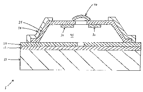
Looking now at Fig. 1, there is shown a tunable
Fabry-Perot filter 5. Filter ~ generally comprises a
substrate 10, a bottom mirror «i mounted to the top of
sL.bstrate 10, a bottom electrode 2~7 mounted t:o the top
of bottom mirror 15, a thin :nenlbrane support 25 atop
bottom electrode 20", a top eaect:rode 30 fixec) to the
underside of thin membrane support 25, a reinforces 35
fixed to the outside perimeter of thin membrane support
25, and a confocal trop mirror 90 se~. atop thin membrane
support 25, with an air cavity 4_'~ being formed between
bottom mirror 15 and top mirror 90.
CA 02411300 2002-11-06
As a result ofthis construction, a Fabry-Perot
filter is effectively created between top m:_rror 40 and
bottom mirror 15. Furthermore, by applying an
appropriate voltage across toy, electrode 30 and bottom
electrode 20, the position of r~op mirror 90 can be
changed relative t<~ bot:tom mirror 1 ~, whereby to change
t:he length of the Fabry-Ps=rcat ~~avi ~y, and hence tune
F~3bry-Perot filtor
Correspondingly, Gnd looking :next at Fig. 2, a
tunable vertical cavity surface emitting laser (VCSEL)
50 can be constructed by positioning a gain region (or
"active region") 55 between bottorrt mirror 15 and bottom
electrode 20. As a result, when gain region 55 is
appropriately stimu:iated, e.g., by optical pumping,
1'i Lansing can be estab:~ished bet:wf:~en t:op mirror 90 and
bottom mirror 15, hurthermore, by applying an
appropriate voltage across top ele~:trode 30 and bottom
electrode 20, the position of top mirror 90 cyan be
changed relative to bottom mirror 15, whereby to change
the length of the laser's reaor:ant cavity, and hence
tune VCSEL 50.
As noted above, tunable Fabry-Perot filters and
tunable VCSEL's of the type disclosed above ~,re
CA 02411300 2002-11-06
advantageous, since they can be quickly and easily
tuned to a desired waveler~g_h by simply changing the
v~ultage applied across the !_o~> electrode and the bottom
electrode.
However, it has also beer. s=ound that tunable
Fabry-Perot filters> and tunable vCSEL's of the type
disclosed above have performance characteristics which
can vary slightly from unit t,~~ unit. In adc.ition, it
has also been found t:hat: t:he per~crrnance
characteristics of any given urui.t= bean vary slightly in
accordance with its age, t:emperature, etc.
Accordingly, s t is ~:leneral.ly n~~>t possible to precisely
predict in advance ivhe exact vc.}lt:age which must be
applied to a particn..llar device iru corder to tune that
device to a specific wavelengt=1~. ';'his can present an
issue in some applications, particularly
telecommunications a:cpplicationa, where the devices may
need to be tuned tr:. precise, known wavelengths (e. g.,
to the ITL WDM grid).
Looking next at: Fig. 3, ttv~ere is shown .3 novel
optical system 100 wr~ich compress's a tunable
Fabry-Perot filter c~r tuzzablo~ vCSEL 105, and which
further comprises a novel ~wavea.engt:h tracker 200 for
CA 02411300 2002-11-06
__
u.se in tuning the t: unable Fabr y-Perot filter or
tunable VCSEL 105 t:o a precisf4, known wavelength.
More particularly, navel optical system 100
generally comprise:.. the tunab:ae Fabry-Perot filter or
tunable VCSEL 105, a pair of: c;ptical fibers 110 and
115, and a pair of collimating lenses 120 and 125.
Where tunable device 105 ~~ornpr~ises a tunable
Fabry-Perot filter, apt:ical fiber 110 might comprise an
input line and optical fiber' 1i.5 rnight comprise an
output line, with the tunable ~ abry-Perot filter
s~2rving to ensure that only light of a selected
wavelength passes from the input lire to the output
lane. Where tunab_1w device 105 comprises a tunable
VSCEL, optical fiber 110 might comprise an input line
to deliver pump light from Gn ;~pt_ical pump laser to the
VC:SEL, and optical ~.i.ber 11' might comprise an output
line for carrying oaf the laser light generated by the
VC:SEL .
The tunable dE:vice is preferably a tunable
Fabry-Perot filter c:ar tunable '~'CSEI_, of the type
disclosed above. Lt: should al.:_~o bE: appreciated,
however, that the tunable Fat~ry-Perot filter or tunable
VCSEL 105 may also c:amprise otrver known types of
CA 02411300 2002-11-06
._
tunable filters arjca tunable Vc_5EL' s compatible with the
~~resent invention.
Novel optical system 100 also comprises the novel
wavelength lackey a00 for use in tuning the tunable
F'abry-Perot filter or tunable VcSEL 105 to a precise,
known wavelength. Waveleng'uh loc);er 200 generally
comprises a beam s~~litter 205 ror tapping a small
amount of the lighr_ emergin<~ froPn tunable dE~vice 105; a
walk-off reflector 210 fo:r diG~.ding the light from beam
splitter 205 into first, record, third and fourth
beams; a multiple etalon ;Z1 'i f~:~r- tai lori ng the light
from the first, second and third beams provided by
walk-off reflector 210; a multiple detector 220 for
detecting the light from t=he first, second and third
beams as they emerge from mu:lr_zple etalon 215 and the
Eight from the four ~2'i beam provided by walk-off
rf~flector 205; and ,:~ control unit: :.'25 for controlling
the tuning voltages applied to tunable device 105
ac: cording 1.o the ou°.puts of multiple detector 220,
whereby to tune tum:~ble device 105 to a precise, known
wavelength .
Beam sp utter 205 comprises a beam sp a tter which
i~; adapted to divert: a small amount of the light
CA 02411300 2002-11-06
- 1.1 w-
emerging from tunable device ls'..~5 to walk-off reflector
210, while still passing t:he great majority of the
light emerging from tunable de:~ice 105 on to optical
fiber 115. By way of example taut: x7ot limitation, beam
s:plitter 205 might divert 2s of tehe light emerging from
tunable device 105 to walk;-c~ff detector 210 while
passing the remaining Q8o of tame light emerging from
tunable device 105 c7n tc:~ optical ffiber 115. Beam
sl?litter 205 preferably has a conventional design of
the sort well known: i.n the art:, except that it is
intended to divert 3 rectangular cculumn of light (i.e.,
a column of light having a rectangular cross-section)
to walk-o.ff reflector 210. To this end, it is
preferred that beam splatter 2_>5 have a working face,
as seen in Fig. 3A, with a rec~:angularly-shaped
reflective surface '.~'05A and nc>~~-reflective surfaces
205B.
Walk--off reflector 210 is shown in greaten detail
in Fig. 4. Walk-off- reflector 210 effectively creates
four parallel beams from the s4ngle beam received from
beam split:ter 205. More partic~ula< 1y, walk-off
rE~flector 210 receives a bean c>f light B~ from beam
splatter 205 and creates a first beam B,, a second beam
CA 02411300 2002-11-06
__ 1 ~
E.2, a third beam B_; and a four;:h beam B'. It should be
appreciated that walk-off rrafi.ector 210 merely divides
the beam B~ into four separar_e beatr~s B;, B,, B3 and B4;
the walk-off reflector dons not affect the ~ravelength
of the light during this beam division. ThL.s, the
wavelengths of beams B,, B_ , 3;; ~3na B~ are identical to
the wavelength of beam 8~..
Walk-off reflector 210 is pi:eferably formed out of
1.261 mm thick fused silica (n = 1.999), with the front
side 230 being caated (x- -- ?8.~$), and the back side
235 being coated (r = 100,), such that the beams walk
o:Ef at a :1 mm spac~_;:~g.
Multiple etalon 215 is sh~awn in greater detail in
F:_g. 5. Multiple e~ralon 215 essentially comecrises
1'i three separate Fabr~,e-Perot eta'ons; a first ~=talon 240,
a second etalon 295 and a third etalon 250.
In general, and loa);ing now at Fig. 6, Fabry--Perot
etalons have a peric:dic transmission profile TP
comprising a plurality of tr,an~>m.ission peaks P spaced
across a range of wavelengt.h:;. It will be appreciated
that the exact locations (i.a~., wavelengths) of these
transmission peaks P are a function of the w~~velength
of the light entering the etalon, and a function of the
CA 02411300 2002-11-06
.~
etalon's substrate thickness <xnd refractive index,
neither of which varies significantly with time.
In accordance with the present invention, first
etalon 290, second etalon 295 and third eta:lon 250 are
fabricated so that there is a r~rewdetermined
relationship betweE:m t:~ein re:~pective transmission
profiles. More particularly, and looking now at Fig.
7, the beam B,' emr>r;lir;g frc~m f i u-~,t: etalan 240 will
have a first transn;ission pro2:ile, the beam B~'
emerging from second etalon 2~~ will have a second
transmission profile which as phasa shifted a quarter
wavelength from the 'transmission profile of the beam
B~' emerg:ing from first etalon 290, and the beam B3'
emerging from third etalon 25G will have a transmission
profile which will consist: of a sinGle transmission
peak within the wavelengths of interest.
Multiple etalorv 215 may bc:~ foz~med in various ways
known in the art. 13y way of example but not
limitation, multipi~:e etalc~n 21'mas;~ comprise a
multilayered dielectric stag: ;~omprisi.ng a base layer
255, a second layer 260 deposited un base layer 255,
and a third layer 2F~5 deposite<~ an second layer 260.
In essence, base layer 255 farTCtS first etalon 240; base
CA 02411300 2002-11-06
._ ,_ 9
layer 255 and second layer ~%6!::~ together form second
etalon 245; and base layer 255, second layer 260 and
third layer 265 tc7c:~ether form third etalon :?50. In one
preferred form of the invention, f:~ase layer 255, second
layer 260 and third layer 265 are all forme<3 out of
Si02.
By placing walk-off reflector %10 and rlultiple
etalon 215 in series, in thc:~ r.anner Shown in Fig. 3,
the beam B, leaving walk-off reflector 210 will be
tailored by the transmission p~ofile of fir~:t etalon
240 so as to create the beam E;'; the beam B; leaving
walk-off reflector 2:10 will ~gy t.ai.lcred by the
transmission profile of second etalon 295 sc as to
cveate the beam 8:~; and the beam Bleaving walk-off
reflector 210 will be tailored by t:he transmission
profile o:E third etalon 250 so as to create the beam
B'.
3
Multiple detector 220 comprises four separate
detectors 270, 275, 280 and 28C:. Multiple detector 220
i~; positioned so tha:~t: the beam B~' falls on detector
270, the beam B;' falls on dE~tector 275, the beam B3'
falls on detector 2f30, and tlue beam B4 (which emerges
directly from walk-off reflectUr 210 and doea not pass
CA 02411300 2002-11-06
__ I 5
through multiple et:.alon 22.0) :alls on detect=or 285.
The outputs I~, I=, I3 and I. are passed from detectors
270, 275, 28G and % 85, resp~=ct: ivel y, to control unit
225.
In this respect it will lr~c appreciated that
inasmuch as the outputs I ; , I.~ and I _: correspond to the
beams B1', B~' and E3' emerging from first etalon 240,
second etalon 295 arid third etalo:~ 250, respectively,
and falling on de t:ectors ?7i., :_'~:~ arid 2fl0,
respectively, outputs I,, I~ arad I ~ wi 11 have an output
profile similar t:o the output tJrof:i.les of the beams
B1' , B2' and B;' , respectively. Compare, for example,
the output profiles of the c>utput_s I,, I and I3 in Fig.
8 to the output pr o f i 1 a s a f the beams B,' , B;' and B3'
in Fig. 7.
On the other hand, it: will also be appreciated
that inasmuch as th~:~ output a~ corresponds to the beam
B4 emerging directly from walk-cuff reflector 210 and
falling directly on detector 285, without passing
through multiple et<:zlon 215, thce output Ia wi.ll have a
substantially flat ~:~rofile, :;,uc_.h as that sho,an in Fig.
8.
CA 02411300 2002-11-06
I6 -
It should also be appreci.atec that the
t:ransmis:~ion profiles shown i:r, F'icxs. 6 and 7, and the
current profiles sloown in F.ig. 8, will vary according
to power. Thus, fc>r example, and looking now at Fig.
9, there are shown, the transm9 ssicn pro =files for a
given etalon at two different power levels.
However, the fact tW t ov:tpuI> is substantially
flat permits the current pr~f:~les shown in ~ig. 8 to be
regularized, i.e., to ire rendered power independent, by
determining the va:Lues (I,!1,,) , (I_/I,l and (I;/I4) .
Thus, and looking now at F'i~~. 1i), there is shown the
regularized, power~-independfmt. cur rent prof.~les
(I,/IQ), (I-=/Iq) and 7;./I4) :~.~~;ic:h correspond to the
beams B~' , B~' and B3' , respectivei°~, er-.e~rging from
first etalon 290, ;~~er_ond E~talc;r~ 295 and third etalon
2.50, respectively.
During initial calibration, control unit 225
rE~ceives the output: I;, I_, I_ and i.~ from the
detectors 270, 275, 2 80 and :?U 5, respectively, and uses
those outputs to build a lookup- t:ak77.e whereby the
control unit 225 ma~,r thereaftetr, daring operation in
the field, tune tun<:~ble devi,:~Ee 105 t.o the desired
wavelength.
CA 02411300 2002-11-06
More particularly, during calibration, tunable
device 105 is swept through a t:~ l~uxning range so as to
successively output: '~~iglt acro,s a range of
w;3velengths. Where tunab7.e devi<°e 7 05 is a tunable
falter, this can bra done by pa:>sing a broad~and light
source into the tunable fi.lter_ whi7_e the tunable filter
i:~ swept across it s t:uninc~ range; ail.ternatively, where
tunable device 105 is a tunable VC:~~EL, this can be done
by sweeping tine VCS~Ia across it::s tuning range while
lasing. Ln either ~:_ase, as A~,~ht:. :is emitted from
tunable device 105 across a rarxgE~ of wavelengths, this
light is simu:ltaneo~.~sly passed (i) to a wavelength
monitor located downstream. of .~ptic~al fiber 115, and
(i.i) into wavelength locker 'G~:~. ~~ontrol unit 225
1-'i builds a lookup table such thaw thEe control unit 225
ma;y thereafter tune tunable device 105 to the desired
wavelength.
In particular, as 'he tunable device is swept
through its tuning range, t:he normalized output (I3/IQ)
is monitored until i.ts peak is encountered; ,~t this
point the device has been t.u;oed ~o a known wavelength
Then, for each wave length ti.a., optical channel)
of interest, its location Cyan be identified along a
CA 02411300 2002-11-06
_. 1 g ...
specific normalized output profile (I,/I4) o.r (Iz/IQ) by
(i) counting the number of perks c>ncounterec~ "up" or
"down" from ~,F, ( i _i > ident:i f yir°sg wO~ether the slope of
that normalized output prof~wle is positive or negative
at that point, and (iii.) identif:;~ina the specific
magnitude of the normalized output (I,/I4) or (I~/Iq) .
This information c:an be recorded in a lookups table
(Fig. 1) stored in control u:it_ <?25.
In theory, it is possible to use just one of the
normalized output profiles II~.'I~j or (I:/I4) , in
addition to the normalized outlout_ I.~rofile (I3/IQ) , to
identify a specific' wavelencth. However, in practice,
it has been found t~.i~at t:he r.orrc~alir.ed output profiles
(I,/I4) and (I,/I~) t:end to have a relative shallow
slope about their pc~dks: as a aesult, a relatively
substantial change in wave~lengt:h may only result in a
very modest change in normali.zE=d output. This can be
difficult to detect and/or reqa..~ire the use of more
sensitive, and hence more expensive, components.
To addre.>s thi:>, it i.s ~~rf~~ferred that at least two
normalized output pr~afiles (~~:/ L4) «nd (I-./IQ) be
provided, where the two normal::zed output pr~~files are
offset from one another by a quarter wavelen~~th. With
CA 02411300 2002-11-06
_ 1 g __
such a construction, one of t: toe normalized ~~utput
profiles will alwa~,is have a s.ignif:icant slope whenever
t:he other of the r7 c:>rmalized o;~tput profiles has a
nominal slope, and vice versa..
During field c:~peration, G.h~=n it is desired to tune
turnable device 1~:'v tc a part..c~.~lar wavelength, the
c.evice is swept thrc~ug:~ it_s ti~:~.ing range as the
normalized output ~;L,;/I:) is m:vnit~red. whe:7 the peak
for the normalized output (l;!:~~) is located, the
tuning voltage is adjusted accwrd.ing to the lookup
table shown in Fig. 1i until t.:~e desired wavelength is
obtained.
By way of example, s~,:ppos~e it is desired to tune
tunable device 105 to optical crhannei "29". First
tunable device 105 is swept through its tuning range
until the peak for the no~maliwed output (I_/IQ) is
encountered. Then, while monit:o~ing the normalized
output (I>/I4), as indicated in the lookup treble for
cizannel 29, the turning vo~:tage i> adjusted so as to (i)
count up two peaks, (ii) bring the slope of the
normalized output ( I /I.: ) neclat ivF= (or falling) and
then (iiil bring ttac-~ normalieci output I:/I~) to a
magnitude of X~4. At this point °::unable device 105
CA 02411300 2002-11-06
aril l be accurately turned to t: he wavelength A~4, i . e. ,
channel 29.
Corresponding:~.y, suppcse it :is thereafter desired
to tune tunable device 105 t:o optical channel "22".
First tunable devi.r~e 105 is swept: through its tuning
range until t:he peak for the ~iormalized output (I3/IQ)
is encountered. Then, wh:il~~ ~r~or.it:oring t=he normalized
output (I,/I4) as indicated in the lookup table for
channel 22, t:he tuning voltaq== is adjusted so as to (i)
count down one peak, (ii) b~i:vg tae slope of the
normalized output ;I,/I.~) pcsit:i~~e (or rising), and
then (iii) bring tt;e normalzzE~d output (I,/I4) to a
magnitude X,~.. At this point t:uruak>le device 105 will
be tuned to the wavelength .h~,, i . c~~. , channel 22.
It will be appreciated that in the foregoing
construction, beam sp utter 2(~5 and walk-of:: reflector
210 essentially serve, collt~ct:ively, as a splitter unit
to tap a portion of the light ~rnerging from tunable
device 105 and create a plu_ality of beams which may
teen be fed into multiple e~aian 21a and multiple
detector 220. However, it :should also be appreciated
that alternative constructicn~. may also be provided.
Thus, for example, the beam sF~:itt.er may be configured
CA 02411300 2002-11-06
_. ~ ,~ _.
to generate a single round column of light, and the
multiple etalon 215 and multiple detector 220 will have
appropriate configurations o as to permit them to
appropriately tailor and det:ec:t portions (e.g.,
quadrants) of that column of: light. Alternatively, the
beam splitter may be configured to generate, and
multiple etalon X15 and multiple detector 2~:0 may be
c~~nfigured to use, a beam ofv 1 ~ght having other
cross-sectional shapes, a"g., E=l.liptical, square or
rectangular, other polygonal shapes, donut ~~hapes, etc.
It is to be understood that. the present invention
i:~ by no means limited t:o the Eu~artlcular cor..structions
and method steps di:aclosed above and/or shown in the
drawings, but also comprises army modificaticns or
equivalents within the scope of the claims.