Note: Descriptions are shown in the official language in which they were submitted.
CA 02411385 2002-12-23
TRANSITION CONTROLLED BALANCED ENCODING SCHEME
CROSS-REFERENCE TO RELATED APPLICATION
This application is related to U.S. Patent No. 5,999,571 issued on December 7,
1999 for an invention entitled "Transition Controlled Digital Encoding and
Signal
Transmission System".
BACKGROUND OF THE INVENTION
Field of the Invention
This invention relates to coding schemes for digital transmission systems.
More
particularly, the present invention relates to a DC-balanced, transition-
controlled coding
system in which an unbalanced datastream is converted to a DC-balanced stream
to
facilitate transmission.
II. Description of the Related Art
As electronic and computer technology continues to evolve, communication of
information among different devices, either situated near by or at a distance
becomes
increasingly important. For example, it is now more desirable than ever to
provide for
high speed communications among different chips on a circuit board, different
circuit
boards in a system, and different systems with each other. It is also
increasingly desirable
to provide such communications at very high speeds, especially in view of the
large
amount of data required for data communications in intensive data consuming
systems
using graphical or video information, multiple input-output channels, local
area networks,
and the like.
CA 02411385 2002-12-23
WO 97136408 PGTlUS97/05220
2.
It is particularly desirable to enable individual personal computers.
workstations, or other computing devices, within which data is normally
internally
transferred using parallel data buses. to communicate with each other over
relatively
simple transmission lines. Such transmission lines typically include only one
or two
conductors. in contrast with the 64-bit and wider data paths within computing
systems now commonly available. In the case of video data transmission to
computer displays, as well as in the case of high-speed video input from
digital
cameras to computer systems, existing interconnection interfaces typically
employ
such parallel data paths. Recently, the requisite bandwidth of such
interconnection
systems has increased as a consequence of increased display resolution. This
has
increased electromagnetic interference f EMI) as well as transmission line
noise,
thereby raising concerns as to safety and reliability. In addition, the large
number
of signal and data lines required by advanced liquid crystal display panels
has
increased the potential for mutual interference.
There have been a number of commercially available products which attempt
to provide high speed conversion of parallel data to serial form and
transmission
over a serial link. The Hewlett-Packard G-link chip set is one such product.
That
chip set includes a transmitter set and is capable of handling 21-bit wide
parallel
data. To obtain the necessary speed. however, the chip set is fabricated using
a
bipolar process. and the receiver and transmitter require separate chips. Such
a
solution is highly power consumptive and expensive.
Another commercial solution has been provided by Bull of France. The Bull
technology employs a frequency multiplier for parallel to serial data
conversion.
Such devices typically introduce noise into the silicon substrate and
interfere with
other multipliers on the chip. In addition, the Bull technology uses an
exclusive OR
tree for parallel to serial conversion. The use of exclusive OR trees is well
known,
together with the difficulty of equalizing the delay through all paths of such
devices.
Additionally, the Hull technology uses output signals having full logic
swings. This
results in slower performance.
CA 02411385 2002-12-23
wo 9~Pcrrtls9~roszzo
3.
Various techniques exist for improving the characteristics of transmission
over serial links. For example, transmission codes may be employed to alter
the
frequency spectrum of the transmitted serial data so as to facilitate clock
recovery
and enable AC coupling. Each transmission code will also typically provide
special
5 characters, not included within the data alphabet, to be used in character
synchronization, frame delimiting, as well as perhaps for diagnostic purposes.
Coding may also be employed to reduce transmission bandwidth as a means of
limiting the signal distortion occurring during propagation through the
transmission
medium. In the case of wire links, it is desirable to utilize codes with no DC
and
10 little low frequency content in order to allow for DC isolation of the
driver and
receiver circuitry from the transmission line, as well as to reduce signal
distortion on
the line. An efficient coding system should also be disposed to encode clock
information with the encoded data in a manner allowing for extraction of the
clock
information during decoding. This obviates the need for provision of a
separate
15 clock signal over a dedicated clock line, since the clock information
recovered
during decoding may be instead used by the receiver circuitry.
Within local area networks (LANs), transmission coding schemes exist for
converting words of various length to characters of greater length. For
example,
three-bit words may be converted to four-bit characters (3B148), four-bit
words may
20 be converted to five-bit characters (4B/SB), and so on. Typically, coding
and
decoding is achieved using a "key" in which each word is mapped to a
corresponding character. Unfortunately, the complexity of this type of mapping
scheme generally precludes utilization of random logic, and often requires
implementations involving look-up cables or the like. This is disadvantageous
given
35 chat look-up tables realized using ROM consume significant chip area and
tend to
slow circuit operation.
- A particular 8B/lOB coding scheme is described in U.S. Patent No.
4.486,739. In particular, a binary DC balanced code and associated encoder
circuit
are described as being operative to translate an 8 bit byte of information
into 10
CA 02411385 2002-12-23
WO 97136408 PCTlUS97/OS220
4.
binary digits for transmission. The 8B/lOB coder is partitioned into a SB/6B
plus a
38/4B coder. Despite ostensibly facilitating DC-balanced encoding, this system
tends to require relatively lengthy encoding and decoding intervals.
Although progress has been made in the development of coding techniques
disposed to facilitate serial data transmission, there remains a need for a
coding
scheme capable of efficiently supporting very high specd serial data
transmission.
Such a coding scheme should also be DC-balanced in order to facilitate AC
coupling
and clock recovery. In addition, it would be desirable to provide a coding
scheme
capable of facilitating real-time data transfer by allowing for rapid
synchronization
10 during decoding. In addition, it would be desirable to provide a coding
scheme
capable of producing a DC-balanced datastream without the necessity of
providing
additional bits to indicate whether a particular block was modified by the
balance-
encoding scheme.
CA 02411385 2002-12-23
5.
SUMMARY OF THE INVENTION
In accordance with one aspect of the present invention there is provided A
method
of producing a transition-optimized DC-balanced sequence of characters from an
input
sequence of data blocks, said method including the steps of:
receiving one input data block from said input sequence of data blocks, said
input
data block consisting of N bits, where N is a positive integer; and
generating a transition-optimized DC-balanced data block from said transition-
optimized data block by determining the number of transitions between adjacent
bits in
the input data block and selectively performing an inversion operation on said
input data
block as a function of said determination in order to produce a transition
optimized data
block, determining a DC-balance of said transition optimized data block,
comparing said
DC-balanced with a previously accumulated DC balance and selectively
performing an
inversion operation on said transition optimized data block as a function of
said
I S comparison, thereby creating said transition-optimized DC-balanced data
block consisting
of fewer than N+2 data bits.
In accordance with another aspect of the present invention there is provided a
method of producing a DC-balanced sequence of characters from an input
sequence of
data blocks, said method including the steps of:
receiving a first input data block in the input sequence of data blocks, said
first
input data block consisting of N bits, where N is a positive integer;
generating a first DC-balanced data block from said first input data block,
said
first DC-balanced data block consisting of at most N bits;
receiving a next input data block in the input sequence of data blocks, said
next
input data block consisting of N bits, wherein N is a positive integer;
generating a next DG-balanced data block from said next input data block, said
next DC-balanced data block consisting of at most N bits; and
combining the first DC balanced data block with the next DC balanced data
block
in order to produce said DC balanced sequence of characters.
In accordance with yet another aspect of the present invention there is
provided an
apparatus for producing a transition-optimized DC-balanced data block from an
input
CA 02411385 2002-12-23
a.
data block, said apparatus comprising:
means for receiving one input data block from said input sequence of data
blocks,
said input data block consisting of N bits, wherein N is a positive integer;
a transition counter for determining the number of logical transitions between
5 adjacent bits in the input data block;
a conditional alternate bit inversion logic for generating a transition-
optimized
data block from said input data block, wherein said conditional alternate bit
inversion
logic inverts a select group of bits within the input data block as function
of the number
of logical transitions determined by the transition counter; and
a DC balancing module for generating the transition-optimized DC-balanced data
block from said transition-optimized data block by comparing a current
disparity with a
cumulative disparity, said transition-optimized DC-balanced data block
consisting of
fewer than N+2 data bits.
In accordance with still yet another aspect of the present invention there is
provided an apparatus for producing a DC-balanced encoded frame from an input
frame
having N bits, where N is a positive integer, said apparatus comprising:
a shift register generator having an output value and N serially coupled
single bit
shift registers, wherein the shift register generator is loaded with a pseudo-
ransom binary
sequence, with each single bit shift having a predetermined value in the
sequence, and
further wherein the contents of each single bit shift register is loaded into
a next higher
order shift register as the shift register generator is clocked with the
contents of a last
single bit shift register in the N serially coupled shift registers being the
output value;
an exclusive-or circuit for combining the predetermined values in a select two
of
the single bit shift registers and loading an output from the exclusive-or
circuit into the
first single bit shift register;
means for receiving and inverting the input frame; and
a selector circuit for selectively outputting one of two inputs with a first
input for
receiving the inverted input frame from the means for inverting and a second
input for
receiving the input frame, wherein the selector circuit is coupled to the
shift register
generator and selectively outputs one o f the two inputs as a function of the
output value.
CA 02411385 2002-12-23
6.
BRIEF DESCRIPTION OF THE DRAWINGS
Additional objects and features of the invention will be more readily apparent
from the following detailed description and appended claims when taken in
conjunction
with the drawings, in which:
FIG. 1 is a block diagram depicting a DGbalanced encoding system of the
present invention implemented within a high-speed digital transmission system.
FIG. 2 shows the overall functional organization of a DC-balanced encoder of
the
present invention in the form of a data flow chart.
FIG. 3 provides a block diagrammatic representation of a decoder included
within
the transmission system of FIG. l .
FIG. 4 shows a random logic implementation of an alternate byte inversion
decoder module of the decoder of FIG. 3.
FIG. 5 is a flow chart depicting the synchronization process effected by a
decoder
synchronization module operative in conjunction with the decoder of FIG. 3.
FIG. 6 is a tlow chart depicting the synchronization process effected by the
decoder synchronization module during high-transition mode operation.
FIGS. 7A and 7B provide a schematic representation of an exemplary
implementation of the encoder.
CA 02411385 2002-12-23
WO 9?136408 PCTIUS9?5220
7.
FIGS. 8A and 8B provide a schematic representation of a prcferred
implementation of the decoder synchronization module.
FIGS. 9A and 9B provide a flowchart representation of an alternative
embodiment of a transition optimizer.
5 FIG. 10 depicts a logic circuit that implcmencs the transition optimizer of
FIGS. 9A and 9B.
FIG. 11 depicts a balance-encoding circuit for DC-balancing a transition-
optimized frame using frame-synchronous scrambling.
FIG. 12 depicts a balance-decoding circuit for decoding a DC-balanced frame
10 encoded with the balance-encoding circuit of FIG. 11.
FIG. I3 depicts a balance-encoding circuit for DC-balancing a transition-
optimized frame using self-synchronous scrambling.
FIG. 14 depicts a balance-decoding circuit for decoding a DC-balanced frame
encoded with the balance-encoding circuit of FIG. 13.
15 DESCRIPTION OF THE PREFER~D EMBODIMENT
I. System Overview
FIG. 1 is a block diagram depicting a transition-controlled, DC-balanced
encoding system of the present invention implemented within a high-speed
digital
transmission system 10. In the system 10 of FIG. 1. 8-hit bytes of parallel
data 14
20 are provided to a DC-balanced encoder 18 operative to effect transition-
controlled.
DC-balanced 8B/ l OB coding in accordance with the present invention. The
resultant
lOB encoded characters 22 are provided to a serializer 26 disposed to convert
the
10-bit characters into a serial data stream for transmission over a serial
data link 30
(e.g., an optical fiber cable. or twisted-pair copper wire). As is described
herein.
25 the relatively straightforward mathematical characteristics of the encoding
algorithm
performed by the encoder 18 allow for economical, high-speed implementations
in
random logic.
CA 02411385 2002-12-23
WO 97136408 PCTlUS97/052Z0
8.
The serial data stream is received from the serial data link 30 by a
deserializer 34 and converted into 10-bit character data 38. The 10-bit
character
data 38 is then decoded into 8-bit data bytes 42 by a decoder 44. As is
described
hereinafter, both the encoder 18 and decoder 4.4 may be economically realized
using
simple digital logic circuits capable of real-time data processing.
II. D_C_-Balanced Transition-Controlled Encoding and Decoding System
The following provides a detailed description of the 8B110B cransition-
controlled coding scheme carried out within the encoder 18. The transition-
controlled code disclosed herein contemplates the use of either a high-
transition or
low-transition set of "in-band" code characters. Each high-transition in-band
code
character is derived from an input data byte in which four or more logical
transitions
exist between the eight bits thereof. Similarly, each low-transition in-band
code
character is derived from an input data byte in which fewer than four logical
transitions exist between its eight bits. This schcme takes advantage of the
fact that
I28 of the 258 eight-bit ASCII codes include four or more logical transitions,
and
the remaining 128 ASCII codes include fewer than four logical transitions.
It has been found that each of the 128 eight-bit codes including fewer than
four logical transitions may be mapped to a corresponding eight-bit code
having four
or more logical transitions. and vice-versa. As is described herein. this
mapping
may be achieved by complementing predefined bits in each eight-bit code to be
mapped. During high-transition mode encoding, the bits within those input
bytes
having fewer than four logical transitions are selectively complemented and
thereby
mapped to bytes having four or more logical transitions. Alternately, during
low-
transition mode encoding the bits within those input bytes having four or more
logical transitions are also selectively complemented and thereby mapped to
bytes
having fewer than four logical transitions. During both encoding modes, a hit
of
predefined value is appended to the selectively complemented byte in order to
produce an intermediate 9-bit encoded symbol prior to creation of a
corresponding
10-bit encoded character. When the input byte includes the number of logical
CA 02411385 2002-12-23
WO 91!36A08 PGT/US9'T105220
9.
transitions mandated by the current encoding mode (i.e. high-transition mode
or low-
transition mode), the appended bit is set to the complement of the predefined
value
in order to identify which of the 9-bit intermediate symbols include
selectively
complemented bytes. This results in the entire set of 256 eight-bit codes
being made
available for encoding into 10-bit characters during both low-transition mode
and
high-transition mode operation.
It may thus be appreciated that each eight-bit code converted into a 10-bit
encoded character during high-transition mode operation includes four or more
logical transitions. Similarly, each eight-bit code converted into a 10-bit
encoded
character during low-transition mode operation includes less than four logical
transitions. These sets of 10-bit encoded characters capable of being produced
during high-transition and low-transition modes of operation may be
characterized as
a high-transition set of "in-band" encoded characters, and a low-transition
set of in-
band encoded characters, respectively. Beyond the 256 in-band characters
within
the high-transition set and the 256 in-band characters of the low-transition
set, there
exists a high-transition sec of 256 out-of-band 10-bit characters and a low-
transition
set of 10-bit characters. In accordance with another aspect of the invention,
various
synchronization and other special characters are defined using the high-
transition and
low-transition sets of out-of-band characters. Each character corresponding to
one
of these "out-of-band" characters associated with the high-transition set
includes less
than four logical transitions, and each of the out-of-hand characters
associated with
the low-transition set of code characters includes more than four logical
transitions.
The difference in the number of transitions between in-band and out-of-band
characters allows selected out-of-band characters to serve as control
characters, and
to be readily distinguished from in-band characters within the transmitted
data
stream.
Given the relatively high number of transitions within each of the in-band
characters of the high-transition set, the high-transition set of characters
may
advantageously be employed to facilitate timing recovery. On the other hand,
the
CA 02411385 2002-12-23
w0 97136408 PCTIUS97/05220
10.
low number of transitions within the code characters of the low-transition sec
makes
this set of characters ideal for use in applications in which it is desired to
minimize
power consumption andJor electromagnetic interference (EMI).
In accordance with one aspect of the invention, the synchronization characters
5 associated with both the low-transition and high-transition sets of code
characters are
selected so as to facilitate rapid synchronization during data recovery. When
the
low-transition set of code characters is being employed, a special group of
out-of-
band characters is used during synchronization. Each special synchronization
character includes a predefined number larger than four (e.g., 7) of logical
ZO transitions between binary character values, and a predefined number (e.g..
two) of
"non-transitions" between character values. As will be discussed below, the
special
synchronization characters are selected such that raadom Logic may be used to
distinguish each special synchronization character from the in-band characters
of the
low-transition set. The following constitutes an exemplary set of out-of-band
15 synchronization characters for use with the low-transition set of code
characters:
1100101010
1101001010
1101010010
1101010100
20 It is a feature of the invention that if one of the above out-of-band
synchronization characters is transmitted three or more consecutive times
within any
preamble period, the synchronization character is ensured of being detected
during
the associated data recovery process. In this regard a "preamble" sequence is
sent
during a preamble period preceding each transmission of encoded characters.
The
25 transmission of preamble sequences may occur not only as part of system
initialization, but also at various ocher times to ensure that synchronization
is
maintained between encoding and decoding processes.
CA 02411385 2002-12-23
WO 97/36408 PCT/US97IOSZZO
11.
The coding scheme of the present invention is predicated on particular
characteristics of the 256 different 8-bit binary code values. Referring to
TABLE I.
the 256 different 8-bit binary codes may be divided into eight groups G0-G7,
where
the binary codes within each group GO-G7 include the same number of
transitions.
It is observed that each binary code within group G0 can be converted to a
corresponding binary code within group G7 by inverting alternate bits within
the
group G0 code. In the same way, each of the binary codes within groups GI, G2
and G3 may be converted to one of the binary codes within groups G6, GS and
G4.
respectively, through inversion of alternate bits. As is described herein. the
high-
transition set of 10-bit characters is obtained by encoding of the 8-bit
binary codes in
groups GO-G3, and the low-transition set obtained by encoding groups G4-G7.
CA 02411385 2002-12-23
WO 97136408 PCT/US97IOSZZO
1'_.
TABLE I
NUMBER OF NZTMBER OF EXAMPLE B~'TES
GROUP TRANSTTIONS BYTES IN GROUP IN GROUP
GO 0 2 00000000. 11111111
GI 1 14 00000001, 11111110
G2 2 42 00000010. 11111101
G3 3 70 00000101, 11111010
G4 4 70 00001010, 11110101
GS 5 42 00010101, 11101010
G6 6 14 00101010. 11010101
I G7 7 ? 01010101, 10101010
During operation of the encoder 18 in a high-transition encoding mode, each
8-bit binary code within byte groups GO-G3 provided thereto is converted to a
corresponding binary code within byte groups G4-G7 through inversion of
alternate
bits. Conversely, during operation in the low-transition encoding mode, each 8-
bit
15 binary code within groups G4-G7 provided to encoder 18 is mapped to a
corresponding binary code within groups G0-G3. In the exemplary embodiment.
the
inversion of alternate bits is effected through the inversion of the even bits
of the 8-
bit binary codes. When the alternate bits of a given 8-bit code have been so
inverted. a predefined bit wnhin the resulting 10-bit encoded character
derived from
CA 02411385 2002-12-23
wo 9~r~6aoa Pcr~trs9~ros~.2o
13.
the given eight-bit code is set so as to indicate that mapping has occurred
between
byte groups.
Referring now to FIG. 2, the overall functional organization of the transition-
controlled DC-balanced encoder 18 of the prcsent invention is shown in the
form of
5 a data flow chart. In FIG. ?, the 8-bit parallel data 14 to be encoded is
latched
within an input latch 70 comprised of, for example, eight D-type flip-flops. A
_ transition counter 74 is operative to count the number of transitions (T) in
logical
value between adjacent bits of each byte of parallel data 14 within latch 70.
If D,.
D6, ... Do, (i.e., D[7:0] comprise the eight bits of data latched within the
input latch
70, then the transition counter 74 may determine T as follows:
T : _ (D7 xor D6) + (D6 xor Dg) + (DS xor D~ + (D4 xor D3)
+ (D3 xor D2) + (D2 xor Dl) + (Dl xor D~)
A COUNT line 78 is set to a predefined logical value by counter 74 if more
four or more logical transitions are counted between bits of the latched byte
(T >
15 3), and is set to the complement of the predefined logical value otherwise
(T <_ 3).
In what follows it will be assumed that COUNT = 0 if four or more logical
transitions are counted by counter 78 (T > 3), and that COUNT = 1 otherwise (T
<_ 3).
As is indicated by FIG. ?. a transition controller 82 is responsive to COUNT
line 78 and to a mode select Iine 86. Mode select line 86 determines whether
encoding is to be performed using the high-transition set or the low-
transition set of
code characters. When mode select line 86 indicates high-transition encoding
is in
effect, and COUNT line 78 registers that less than four logical transitions
exist
within the byte stored within latch 70. the transition controller 82 instructs
w25 conditional alternate bit inversion (CABI) logic 90 to invert the even
bits the byte
stored within latch 70. The resultant conditionally inverted byte, which will
have
four or more logical transitions, is stored within intermediate latch 94.
Conversely,
CA 02411385 2002-12-23
WO 97/36408 PCT/US97JOSZ20
14.
if high-transition encoding is in effect and four or more logical transitions
are
counted within the byte stored in the input latch 70, the transition
controller 82
causes CABI logic 90 to simply transfer the byte from latch 70 (without bit
inversion) to the intermediate latch 94. Accordingly, during high-transition
encoding
mode,
if T < 4,
then E[8:0) _ ' 1' D~D6DgD4D3D2D1D0,
else if T ? 4,
then E[8:0] _ '0' D~D6D5D4D3D'DIDo
where E[7:0] comprise the eight bits stored within the intermediate latch 94,
and
E[8] comprises the value of COUNT stored within COUNT latch 95.
When mode select line 86 indicates that low-transition encoding has been
selected, and COUNT line 78 registers that four or more logical transitions
are
present within the byte stored within latch 70, the transition controller 82
instructs
conditional alternate bit inversion (CABI) logic 90 to invert the even bits
the byte
stored within latch 70. Otherwise, if low-transition encoding being performed
and
four or more logical transuons are counted within the byte scored in the input
latch
70, the stored byte is simply transferred without bit inversion to the
intermediate
latch 94. Accordingly, during low-transition encoding mode.
if T > 3, then E[8:0) _ ' 1' D7D6DgD~D3D~DIDp,
else E[8:0) = '0' D~D6D5D4D3D~DIDo
After CABI logic 90 has provided a byte having a number of logical
transitions within the appropriate range to latch 94, a DC-balancing process
is
performed in which the cumulative disparity between complementary logical
values
within the stream of 10-bit encoded characters produced by the encoder 18. As
used
CA 02411385 2002-12-23
WO 97/36408 PGTlUS97I05220
15.
herein. the term "cumulative disparity" (D~,m) denotes the excess of one bits
relative
to zero bits produced by the encoder 18 subsequent to synchronization being
achieved with the decoder 44 in the manner described below. The teen "current
disparity" (D~,f) refers to the excess of one bits to zero bits within the
byte cutTentlv
stored within the latch 94. and is determined by disparity checkcr 96. A DC-
balancing module 98 serves to compare the current disparity to the cumulative
disparity stored within latch 99. The result of the comparison is then used to
determine whether the byte stored within latch 94 is inverted by conditional
byte
inversion (CTBI) logic 100 during the course of transfer thereof to output
register
104. In this way CTBI logic 100 serves to minimize the cumulative disparity
associated with the serial stream produced by the encoder 18. The following
provides a logical description of the manner in which each of the 10-bit
characters
T[9:0] in the DC-balanccd character stream produced by the encoder are derived
from the byte E[7:0] stored within the intermediate latch 94 and the bit E[8]
within
1 ~ COUNT latch 95 .
The current disparity (DNr) is computed by the disparity checker 96 as
follows:
D~"! : _ { (F.~ and E6) ~ f ES and E,~) + (E3 and E-,) + (E 1 and Ep) }
- {(E~ nor E6) + (ES nor E,~) + (E3 nor E2) + (E1 nor EO)}
Ii is noted that during operation in the high-transition mode, -2 <_ D~,m <_
2, while
during operation in the low-transition mode -4 <_ DP <_ 4. Within the DC
balancing module 98, if it is determined that DNr = 0 or D~,m = 0, then
if Eg = '0'
then T[9:0] _ ' I' EgF~E6EgEQE3E2E 1 Ep, and
25
D ~ cum = Dcum - Dour
else if Eg is not equal to zero,
then T[9:0] _ '0'EgE.~E6EgE4E3F~EtEp, and
CA 02411385 2002-12-23
wo 9~r~6aos Pcr~s9~roszzo
16.
D'~m=D~"",+D«~~
where D'~m is the updated cumulative disparity computed by disparity updater
108
and stored thereby within latch 99.
Alternately, if the DC-balancing module determines that the most significant
bit
(MSB) of DN~ and the MSB of D~"~ are not equivalent. then
T[9:0]='0'EgF~E6E5E4E3E'EIEp, and
D'«, = D~~ ~". DN~ - Eg
Finally, in all other cases if the MSB of D~ and the MSB of D~ are equivalent,
then, then
10 T[9:0] _ ' 1'EgE7~fi~gE4E3F.~EIF.p. and
D'~m = D~m - DNW' E8
In this way the cumulative disparity is reduced, and DC balance achieved.
through selective inversion of the byte E[7:0] by CBI logic 100 during the
course of
filling the output latch 104 as T[7:0]. It is observed that the logical value
of T[8] is
15 indicative of whether the even bits of byte D[7:0] received at input latch
70 were
complemented during generation of the byte E[0:8]. Similarly, the logical
value of
T[9] indicates whether byte E[7:0] was inverted during transfer to latch 104.
III. Decoding
Referring to FIG. l, the deserializer 34 receives the sequence of 10-bit
20 characters T[9:0] produced by the encoder and generates 10-bit paralle!
received data
upon bit lines RX9, RXa, ..., RXo (i.e., RX[9:0]). This 10-bit parallel
received data
is provided over bit lines RX[9:0] to the decoder 4.4, as well as to a decoder
synchronization module 114. As is described below in section IV, the
synchronization module 114 is operative to ascertain boundaries within the 10-
bit
CA 02411385 2002-12-23
WO 97136408 PGTIUS97IOSZ20
17.
parallel received data corresponding to the frame boundaries of the
transmitted data
(i.e., to T[9:0]). Specifically, synchronization module 114 determines upon
which
of the bit lines RX[9:0] the deserializer 34 is providing the received bits
corresponding to the first bit T[0] of each transmitted byte T[9:0]. Upon
making
this determination, the synchronization module 114 provides a frame boundary
pointer 118 to decoder 44 identifying the one of the bit lines RX[9:0]
corresponding
to the first bit T[0] of each transmitted 10-bit character T[9:0]. Upon
receiving this
synchronization information. the decoder 44 is disposed to decode the received
data
RX[9:0] in the following manner.
10 FIG. 3 provides a block diagrammatic representation of the decoder 44. The
10-bit parallel data produced by the deserialiter is seen to be received over
bit lines
RX[9:0] by a decoder switch 150. The decoder switch 150 serves to switch the
10-
bit data received over bit Lines RX[9:0] to switched bit Lines S[9:0] in
accordance
with frame boundary pointer value 118 provided by the synchronization module I
14.
Specifically, the one of the received bits RX[9:0] corresponding to the first
transmitted bit T[0] is switched to bit line S[0], the one of the received
bits RX[9:0]
corresponding to the second transmitted bit T[1] is switch to bit line S[1],
and so on.
The switched data impressed upon bit lines S[7:0], which coitesponds to the
transmitted data byte T[7:0), is stored within 8-bit latch 154. Similarly, the
20 switched data bit S[8], which corresponds to the transmitted bit T[8], is
provided to
1-bit latch 158. Since the logical value of bit line S[8] tracks the logical
value of
T[8], the bit line S[8] informs the Alternate Bit Inversion (ABI) decoder 160
as to
whether the even bits of the input data D[7:0] were complemented by CABI logic
90
(FiG. 2) during the encoding process. Likewise, the bit line 5[9] (which
tracks the
25 logical value of T[9]) informs the ABI decoder 160 as to whether CTBI logic
100
complemented the byte scored within latch 104 during the DC-balancing portion
of
the encoding process. In this way the decoder 160 is informed of the logical
operations performed upon the byte S[7:0] stored within 8-bit latch 154 during
the
encoding process, thereby facilitating straightforward decoding using random
logic.
CA 02411385 2002-12-23
WO 97!36408 PCTIU597/OSZ20
18.
Turning now to FIG. 4, there is shown a random logic implementation of the
ABI decoder i60. The ABI decoder includes a set of nine exclusive-or (XOR)
sates
N1-N9 for decoding the 10-bit frame-aligned data S[9:0] in order to produce
the 8
bit decoded byte DE[7:0]. In the implementation of FIG. 4, the XOR gates N1-N9
5 produce the decoded byte DE[7:0] as follows:
DE[7] : = S[7] xor S[9]
DE[6] : = S[6] xor (3
DE[5] : = S[5] xor S[9]
DE[4] : = S[4] xor l3
DE[3] : = S[3] xor S[9]
DE[2] : = S[2] xor Q
DE[1] := S[1] xor S[9]
DE[0] : = S[0] xor a
where (3 : = S[9] xor S[8].
IV. Synchronization
As mentioned above, the decoder synchrotuzation module 114 provides an
indication to the decoder 44 of the frame boundary of each transmitted 10-bit
character T[9:0]. The decoder module 114, together with the decoder switch 150
(FIG. 3), effectively function as a barrel-shifter to shuffle the parallel
data RX[9:0]
20 from the deserializer into the frame-aligned data S[9:0]. In accordance
with the
invention, a preamble sequence is produced by the encoder 18 at various times
(e.g.,
at system power-up) in order to facilitate frame boundary deoection by the
synchronization module 114. In the exemplary embodiment this preamble sequence
includes several repetitions of selected out-of-band characters easily
distinguishable
~5 from in-band characters. Again, during high-transition mode operation each
out-of
band character will include less than four logical transitions, and during low
CA 02411385 2002-12-23
wo s~r~saos pcrrus9~roszzo
19.
transition mode operation each out-of-band character will includes four or
more
logical transitions. As is discussed below, during operation in each mode
several
repetitions of specially selected out-of-band characters are produced by the
encoder
18 during the preambling period as a means of ensuring rapid frame boundary
identification within the decoder synchronization module 114. At the
conclusion of
the preambling period, the module 114 will "know" which of the bit lines
RXj9:0)
corresponds to the first bit Tj0] of the 10-bit transmitted character, and
will inform
decoder via frame boundary pointer 118.
By selecting an appropriate subset of out-of band characters for transmission
during the preambling period, the worst-case time required for synchronization
to be
achieved may be reduced relative to that required by conventional
synchronization
schemes. In particular, during low-transition mode operation the following out-
of-
band characters are used as "synchronization characters".
1100101010
1101001010
1101010010
1101010100
During high-transition mode operation, the following out-of-band characters
are used as svnchronizauon characters:
1000001111
1000011111
1000111111
1001111111
1011111111
_25 During each preambling period, three repetitions of the same
synchronization
character are produced by the encoder 18. As is described herein, by
processing the
21 bits most recently produced by the encoder 14, synchronization module 114
is
CA 02411385 2002-12-23
wo 9~r~Eaos rcrws9~rosizo
20.
able to detect at least one of the three repetitions of the synchronization
character
transmitted during a given preambling period. This advantageously allows
synchronization to be achieved within a relatively short preambling period.
Turning now to FIG. 5, a flow chart is provided of the synchronization
S process effected by the decoder synchronization module 114 during low-
transition
mode operation. During each clock cycle of the module 114, a block of ten bits
is
loaded from the deserializer 34 into a first 10-bit latch 150. Also during
each clock
cycle, a 10-bit block is transferred from the first 10-bit latch 150 to a
second 10-bit
latch i54. Similarly, the 10-bit block currently stored within the second 10-
bit latch
154 is transferred during each clock cycle to a third 10-bit latch 158.
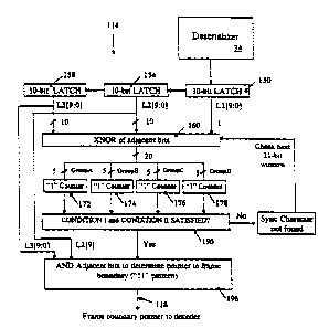
As is indicated by FIG. S, an exclusive-NOR (XNOR) operation (step 162) is
performed between adjacent bits included within a 21-bit "window" of data held
by
the latches 150.154,158. Specifically, this 21-bit window includes a 10-bit t
k
L3[9:0] from the third latch 158, a 10-bit block L2[9:0] froth the second latc
~4,
15 and the bit L1[9] from the first latch 150. In this regard the bit Ll[9] is
that bit
which becomes bit L2[9) upon being transferred to the second latch 154. As an
example of operation during the low-transition mode, consider a 21-bit window
(i.e.,
L3[9:0], L2[9:0], L1[9]) comprised of the following parallel bit sequence:
101101001010110100101
If an XNOR operation is performed between each pair of adjacent bits, the
following result is obtained:
00100010000010001000
As is indicated by FIG. 5, this 20-bit result of the XNOR operation (step
160) is divided into four 5-bit groups (i.e., Group A, Group B, Group C and
Group
D). In the current example, these four 5-bit groups are defined as follows:
OO1000100000I0001000 Result of XNOR operation}
CA 02411385 2002-12-23
WO 97136408 PCT/US97/05220
21.
00100 {Group A}
01000 {Group B}
00100 { Group C }
01000 {Group D}
The synchronization characters for both the high-transition mode and the low-
transition modes enumerated above have been selected such that particular
relationships arise between Groups A, B. C and D during the preambling period.
That is, when three consecutive occurrences of the same synchronization
character -
produced by the encoder 18 during preambling - are received by the
deseriaiizer 34
and provide as 10-bit parallel data to the synchronization module 114.
In an exemplary implementation, the following two relationships (Condition I
and Condition II) arise between Groups A. B, C and D during the preambling
period:
Condition I. The number of logical "I's" collectively present in Groups
A, B, C, and D is exactly four, and corresponds to one of the following
three cases:
Number of Logical I's
Case ou A Group B Gr a Groun D
#1 1 1 1 1
#2 2 0 2 0
#3 0 2 0 Z
As is indicated by FIG. 5, the number of "1's" in each of the Groups A, B. C
and D are determined by " 1 " counter modules 172. I74, 176 and 178,
respectively .
Since the number of "I's" within each Group A. B. C and D is determined by the
25 results of the XNOR operation between adjacent bits in the 21-bit window
(step
160), the number of "I's" within each group is indicative of the number of
"non-
transitions" in logical value between adjacent bits in each of four segments
of the
21-bit window associated with Groups A. B, C and D. In the current example, it
is
CA 02411385 2002-12-23
WO 97136408 PCTIUS97IQ5220
seen that each of Groups A, B. C and D each include a single " 1 " .
Accordingly,
the current example corresponds to Case #l.
Conditaor~ II. The sequence of bits comprising Group A is equivalent to
the bit sequence of Group C, and the sequence of bits comprising Group
5 B is equivalent to the bit sequence of Group D. That is, Group A =
Group C, and Group B = Group D.
In accordance with the invention, both Condition I AND Condition II are
satisfied if and only if the same synchronization character is stored within
the first,
second and third 10-bit latches 150. 154 and 158. That is, both Condition I
and
10 Condition II are satisfied only during the preambling period, when three
repetitions
of the same synchronization character are produced by the encoder 18. This
aspect
of the invention is explained immediately below with reference to low-
transition
mode operation.
As was described above, the adjacent bits within a 21-bit window provided by
15 latches 150, 154 and 158 are XNOR'ed during step 160 (FIG. 5). Because each
in-
band or out-of-band character produced by the encoder 18 is exactly ten bits
in
length. the 21-bit window will include all or part of 1s', '_'"° and
3T° 10-bit characters.
The various ways in which the ? 1-bit window may include bits from these 15',
2"°
and 3~° 10-bit characters is sec forth below:
20 # Of Bits
CA 02411385 2002-12-23
WO 97136408 PCTlUS9?/05220
~3.
1" '~ 3=
racter Character C arac
er
1 10 10
2 10 9
3 10 8
4 10 7
10 6
6 10 5
7 10 ~t
8 10 3
9 10 2
10 10 1
Since each character is either an in-band (e.g., DATA) character or an out-
of-band command or synchronization (i.e., SYNC) charactrer, the following sets
15 forth the possible combinations of DATA and SYNC characters among the 1s',
2'~
and 3'° 10-bit characters contributing to the 21-bit window:
1...'
Combination Character C cter acter
A SYNC SYNC SYNC
B SYNC SYNC DATA
C SYNC DATA DATA
D DATA DATA DATA
E DATA DATA SYNC
F DATA SYNC SYNC
For example, the 2I-bit window could be comprised of two bits of a 1s'
SYNC Character, ten bits of a 2"° DATA Character, and nine bits of a
3~° DATA
Character (i.e., Combination C).
During low-transition mode operation, all in-band (e.g., DATA) characters
include a maximum of three logical transitions or, equivalently, more than
four
"non-transitions" in logical value between the ten adjacent bits of the in-
band
30 character. Accordingly, during low-transition mode operation if the
2"° character is
a DATA character, it wilt include more than four logical non-transitions.
Since
CA 02411385 2002-12-23
WO 97/36408 PCTlUS97lO5Z20
24.
Condition I indicates that the number of logical non-transitions within the
entire 21-
bit window will be exactly four when three identical SYNC characters are
present
therein, Condition I wil! not be satisfied when the 2"° character is a
DATA character
since it would include more than four logical non-transitions. Hence, if
Condition I
is to be satisfied then the Z1-bit window cannot be comprised of the character
sets
specified by Combinations C, D and E (i.e., ~"° character is a DATA
character).
In accordance with the invention, the synchronization characters listed above
have been chosen such that Condition II will be satisfied if the 1u and
3'° characters
transmitted during any preamble period are identical. Hence, Combination B and
F
do not satisfy Condition II. It follows that only Combination A (i.e., three
consecutive SYNC characters) satisfies both conditions I and II.
Referring to FIG. 5, if both Condition l and Condition II are satisfied (step
190) then selected adjacent bits within Groups A and B are AND'ed (step 196)
as
described below in order to identify the frame boundaries of the SYNC
characters
detected within the 21-bit window. Since each SYNC character within the 21-bit
window is loaded by the deserializer 34 into latch 150, the frame boundary of
each
SYNC character may be identified in terms of the one of the bit lines R[9:0]
from
the deserializer 34 upon which the first bu of each such SYNC character is
impressed. Once this idernification is achieved, the decoder ~ is informed of
the
identity of this bit line R[9:0] by way of frame boundary pointer 118.
The AND operation of step 196 is performed between all of the adjacent bits
in the third latch 158 (i.e., L3[9:0]), as well as between L3[0] and L2[9].
When the
result of step 190 has indicated that both Condition I and Condition II are
satisfied.
the result of the AND operation of step 196 will produce only a single logical
one
indicative of the value of the frame boundary poimer 118. In the current
example,
- L3[9:0] : _ { 1011010010} and L2[9] : =[1], and thus the result of the AND
operation of step 196 is {0010000000}. That is, the third position in the 21-
bit
window corresponds to the first bit of a synchronization character.
Accordingly, in
CA 02411385 2002-12-23
wo 9~r~~ Pcr~s9~rosJ.zo
25.
the current example the frame boundary pointer 118 would be set so as to
identify
the third (RX[7]) of the ten bit lines RX[9:Oj as carrying the first bit of
each 10-bit
character produced by the deserializer 34.
In the exemplary embodiment a preambling sequence (i.e., three repetitions
of the same out-of-band SYNC character) is sent upon system power-up as well
as
during lapses in data transmission over the serial link 30. This allows timing
synchronization to be maintained between the encoder 18 and decoder 4.4 even
in the
absence of data transmission for extended periods.
FIG. 6 is a flow chart depicting the synchronization process effected by the
decoder synchronization module 114 during high-transition mode operation. As
is
indicated by FIG. 6, the high-transition mode synchronization process is
substantially
similar to that performed during low-transition mode operation (FIG. S). In
particular, the high-transition mode synchronization process differs from the
low-
transition mode synchronization process primarily in that:
(l) In step 160', an exclusive-OR (XOR) rather than an exclusive-NOR
(XNOR) operation is performed upon adjacent bits within the latches 150', 154'
and
158' .
(ii) In step 196'. an AND operation is performed between each bit and the
complement of the bit immediately to the right (e.g., L3[9] AND L3[8], L3[8]
AND
L3[7], L3[7] AND L3[6], and so on. In this way the AND gate producing a
logical
" I " identifies a " 10" or "falling edge" sequence corresponding to the frame
boundary .
V. Hardware Ir~,glementations of Encoder and Decoder Synchronization
dule
In this section a description is provided of a specific hardware
implementation of the encoder 18, and of an implementation of the decoder
synchronization module 114 suitable for use during low-transition mode
operation.
CA 02411385 2002-12-23
wo 9~r~s~os rerrtJS9~roszzo
26.
A description of an exemplary hardware realization of the decoder 4.4 in
random
logic was provided above in section III.
FIGS. 7A and 7B provide a schematic representation of an exemplary
implementation of the encoder 18. The 8-bit parallel data D[7:0] from latch 70
to
be encoded is seen to be provided to seven exclusive-OR gates 240 of the
transition
counter 74. The outputs of the exclusive-OR gates 240 are provided to a set of
full-
adders 242, 244. 246 and 248. The carry output (C) of the full-adder 248
corresponds to the COUNT Iine 78, and indicates whether less than four logical
transitions exist between the bits in the data D[7:0]. When an out-of-band
command
is being received from latch 70, a command line (TX CMD) provided to NOR gate
260 is raised so as to prevent the COUNT Iine 78 from causing inversion of the
even bits of D[7:0] within CABI logic 90. Otherwise, when the data D[7:0] from
latch is being encoded in accordance with the invention, the output 78' of NOR
gate
260 tracks the logical value of COUNT line 78.
15 As is indicated by FIG. 7A, in the exemplary embodiment CABI logic 90 is
comprised of a plurality of NOR gates 270. Each NOR gate 270 includes one
input
coupled to COUNT Line 78' . and another input connected to one of the even
bits of
D[7:0]. The output of CABI logic 90 is provided to intetinediate latch 94,
which is
coupled to the input of disparity checker 96 (FIG. 7B).
20 Turning to FIG. 7B, the disparity checker 96 includes four AND gates 290-
293 for determining occurrences of "II" within the conditionally bit-inverted
byte
E[7:0]. Similarly, four NOR gates 296-299 are provided for detecting
occurrences
of "00" within E[7:0] . Since pattern of "O1 " and "O1 " within E[7:0] are
already
"DC-balanced" in the sense of including equal numbers of ones and zeroes,
there
25 exists no need to detect such patterns during the DC-balancing process
effected by
the circuitry of FIG. 7B. A first full-adder 302 and first half adder 306 are
disposed
to count the occurrences of " 11 " detected by AND gates 290-293. In like
manner a
second full-adder 308 and second half-adder 312 are provided for counting the
CA 02411385 2002-12-23
WO 97I3b408 PGT/US97/OSZZO
27.
occurrences of "00" detected by the NOR gates 296-299. A first pair of full-
adders
316 and 318 determine the difference in the counted occurrences of " I 1 " and
"00" .
The DC-balancing module 98 includes a three-input NOR gate 330, a first
exclusive-OR gate 332. a latch 336 and a second exclusive-OR gate 338. When
the
occurrences of " 11 " and "00" are determined to be equivalent by full-adders
316 and
318, the complement of E[8] determines the value of T[9], and hence whether
the
byte E[7:0] is inverted by CTBI logic 100. When the counted occurrences of
"00"
and " 11 " are not equivalent, the value of T[9] comprises the output of XOR
gate
332. In this regard a first input 342 to XOR gate 332 comprises the most
significant
bit (MSB) produced by the pair of full-adders 316 and 318, which is equivalent
to
the MSB of the current disparity DNf (i.e.. the difference in "1's and "0's"
in
E[7:0]). A second input 344 to XOR gate 332 corresponds to the MSB of the
cumulative disparity D~"". As is indicated by FIG. 7B, the latch 99 for
storing the
cumulative disparity is comprises of three registers 350-352. The cumulative
disparity is updated by a disparity updater 108 comprised of a backward chain
of full
adders 356 and 358, a set of three exclusive-OR gates 360-362, and a
corresponding
sec of three full-adders 365-367. Finally. CTBI logic 100 includes a sec of
eight
exclusive-OR gates 374.
FIGS. 8A and 8H provide a schematic representation of a preferred
implementation of the decoder synchronization module 114. In FIG. 8A, the 10-
bit
latches 150, 154 and 158, for storing L3[9:0], L2[9:0] and L1[9:0],
respectively,
may each be realized using an array of ten D-type flip-flops. A plurality of
XNOR
gates 402 are provided for XNOR'ing adjacent bits included within the 21-bit
window corresponding to L3[9:0], L'?[9:0] and 11[9]. The Group A, Group B,
Group C, and Group D outputs of the XNOR gates 402 are then respectively
provided to the "1" counters 172. 174, 176 and 178. As is indicated by FIG.
8A,
the existence of Condition I is detected by random logic 190a, which is
comprised of
_ four NAND gates 410-413.
CA 02411385 2002-12-23
WO 97136408 PCTlUS9?/05220
28.
Turning now to FIG. 8B, the existence of Condition II is identified by an
arrangement of random logic identified by reference numeral 190b. Random logic
190b includes a set of ten XOR gates 422, the outputs of which are provided as
shown to NAND gates 426 and 428. The outputs of NAND gates 426 and 428 are
5 coupled to the inputs of a NOR gate 430, the output of which is driven to a
logical
"1" when Condition II is satisfied. Finally, the logical state of the output
(Sync Sig)
of an AND gate 440 is indicative as to whether Condition I and Condition II
have
been satisfied (i.e.. as to whether synchronization has been achieved). If so,
adjacent bits within L3[9:0] and L2[9] are AND'ed (step 196 of FIG. 5) by a
set of
10 ten AND gates 450. The outputs PTR[9:0] comprise the frame boundary pointer
118, which informs decoder 44 as to which of the bit lines RX[9:0] correspond
to
the first bit T[0] of each transmitted l0.bit character T[9:0] .
~JI. Alternate Embodiments
Transirion optimization based on 1-bit cowu
15 Figures 9A and 9B are flowcharts depicting an alternative encoding
technique
for producing a transition-optimized signal stream.
Referring to the flowchart of Figure 9A, during a transition minimization step
SOIa an input frame of data. such as the 8-bit frame D[0:7] 503x, is processed
as
described below. Specifically, in step SlOa. the number of bits set to in "1"
in
20 frame 503a are counted. The count value is depicted in the flowchart as "S"
. In
step S 15a, the count is compared to a predetermined threshold value that
represents
one-half of the frame size. Thus, for an 8-bit frame, the count is compared to
the
value 4.
- If the count value exceeds 4, in Step 520a a 9-bit transition-minimized
frame
25 is formed by performing a NRZIo-encoding operation over 8-bit frame D[0:7]
and
prepending a '0' bit in order to form transition-minimized frame E[0:8J 504a.
The
CA 02411385 2002-12-23
wo 9~pcrws9~roszzo
29.
NRZIo-encoding operation consists in part of setting the low-order bit E[O] of
frame
504a to the value of the high-order D[0] bit of frame 543a. In addition, each
bit
E[1] through E[7] in frame 504a is obtained by performing an XNOR operation
using the corresponding bit in D[1] through D[7] in frame 503a and the next-
higher-
5 order bit, and finally by prepending a binary '0'. That is, to produce an
NRZIo-
encoded 9-bit frame from an unencoded 8-bit frame:
E[D] < - D[O]
E[1] < = D[0] XNOR D[1]
E[2] < = D[1] XNOR D[2]
...
E[6] < = D[5] XNOR D[6]
E[7] < = D[6] XNOR D[7]
E[$] < _ ,0,
If the count value derived in Step S 10a is less than 4, in Step 521 a 9-bit
transition-minimized frame is formed by performing a NRZI,-encoding operation
over 8-bit frame D[0:7] 503a and prepending a ' 1' bit to form transition-
minimized
frame E[0:8] 504x. The NRZI!-encoding consists of setting the low-order bit
E[0]
of frame ~04a to the value of the high-order D[0] bit of frame 503a. Moreover,
each bit E[ 1 ] through E[7] is sec to a value determined by performing an XOR
20 operation using the corresponding bit D[1] through D[7] in frame 503a and
the next-
higher-order bit, and finally by prepending a binary ' 1' . That is, to
produce an
NRZI,-encoded 9-bit frame from an unencoded 8-bit frame:
E[0] < = D[0]
E[1] < = D[0] XOR D[1]
E[2] < = D[1] XOR D[2]
E[6] < = D[5] XOR D[6]
E[7] < = D[6] XOR D[7]
CA 02411385 2002-12-23
WO 97/36408 PGTlUS97/OSZZO
30.
E[8] ~ _ .1,
If the count value derived in Step 510a is equal to 4, then in Step 5I7a the
value of D[O) is used to select whether transition-minimized frame 504a is
formed
by NRZIo-encoding or NRZI,-encoding. If D[0] is equal to '1', transition-
minimized
5 frame 504a is formed by NRZIo-encoding frame 503a in Step 520a. If D[0] is
equal
to '0', transition-minimized frame 504a is formed by NRZI,-encoding frame 503a
in
Step 521.
Figure 9B depicts a flowchart of an encoding process or producing a
transition-maximized signal stream. The transition-maximization process SOIb
of
10 Figure 9B is simiiar to the transition-minimization process of Figure 9A,
except that
the positions of the NRZTa-encoding and NRZI,-encoding blocks are swapped.
In step 510b, the number of bits in 8-bit frame D[0:7] which are sec to "1"
are counted. The count value is depicted in the flowchart of Figure 9B as "S".
In
step 515b, the count is compared to a predetermined threshold value that
represents
15 onc-half of the frame size. Thus, for an 8-bit frame, the count is compared
to the
value 4.
If the count value exceeds 4. In Step 521b a 9-bit transition-maximized frame
is created by performing a NRZI,-encoding opcration over 8-bit frame D[0:7]
503a
and prepending a ' I' bit, thereby forming transition-maximized frame E[0:8)
504b.
20 The NRZI,-encoding consists of setting the low-order bit E[O] of frame 504b
to the
value of the high-order D[O) bit of frame 503b. and setting each bit E[1]
through
E[7] to a value determined by XOR'ing the corresponding bit D[0:7] in framc
501b
and the next-higher-order bit. A binary ' 1' is then prtpendended to the
resulting set
of bits.
25 If the count value derived in Step S l Ob is less than 4, in Step 520b a 9-
bit
transition-maximized frame is formed by performing a NRZIo-encoding operation
CA 02411385 2002-12-23
WO 97136408 PGT/US97/05220
31.
over 8-bit frame D[0:7] and prepending a '0' bit to form transition-maximized
frame
E[0:8] 504b. The NRZI"-encoding consists of setting the low-order bit E[0] of
frame 504b to the value of the high-order D[0] bit of frame 503b, and setting
each
bit E[1] through E[7] to a value determined by XOR'ing the corresponding bit
D[0:7] in frame SOIb and the next-higher-order bit. A binary '0' is then
prepended
to the resulting set of bits.
If the count value derived in Step S lOb is equal to 4. Step 517b selects
whether transition-maximized frame 504b is formed by NRZIo-encoding or NRZI,-
encoding depending on the value of D[0]. If D[0] is equal to ' 1', transition-
10 maximized frame 504b is formed by NRZI,-encoding frame 503b in Step 521b.
If
D[O] is equal to '0', transition-maximized frame 504b is formed by NRZIo-
encoding
frame 503b in Step 520b.
Fig. 10 depicts a logic circuit 530 that implements the transition
optimization
operations of Figs. 9A and 9B. As shown in Fig. 10, 8-bit frame 503 is
presented
to counter 532. Counter 532 calculates the number (N,) of ' 1' bits and the
number
(No) of '0' bits (not shown) in frame 503, and presents these counts to mode
selector
534. Mode selector 534 calculates two logical values. The first logical value
represents the conditions 515b. 516b and 5I7b used in selection of the NRZI<,-
encoding step ~20b of transinon-maximizer ~Olb. and is represented by the
logical
value
[(N, .GE. 5) + ((N, .EQ. N~ .EQ. 4) x (D[0] .EQ. 0))].
The second logical value represents the conditions S 15a, 516a and 517a used
in
seleeuon of the NRZIa-encoding step 520a of transition-maximizer 501a, and is
represented by the logical value
[(No .GE. 5) + ((N, .EQ. No .EQ. 4) x (D[0] .EQ. 1))].
CA 02411385 2002-12-23
WO 97!36408 PC'l<'tLTS97/05220
32.
Mode-selection signal 536 (labeled "MAX") is selectively set to '0' to select
transition-minimized optimization, or is set to ' 1' to select transition-
maximized
optimization. Mode selector 534 uses MAX to select one of the two calculated
logic
values, which results in control signal 535 (labeled "CONT") selecting between
5 NRZIa and NRZI, encoding.
8-bit frame 503 is presented as input to an array of XNOR gates 538-1
through 538-7, and also to an array of XOR gates 539-1 through 539-7. XNOR
gates 538-1 through 538-7 perform NRZlq encoding over frame 503 and present
the
resulting signals, along with '1' bit 541, as input to selector 542. XOR gates
539-1
10 through 539-7 perform NRZI, encoding over frame 503 and present the
resulting
signals, along with '0' bit 540, as input to selector 542. Selector 542
selects
between the NRZIo-encoded signal and NRZI,-encoded signal in accordance with
control signal 535, and produces as output the 9-bit transition-optimized
signal 504
E[0: 8] . The transition-optimized signal thus formed may be decoded using the
same
15 general method and apparatus discussed in connection with Figs. 3 and 4,
above.
Frame-wise DC-6atancing using a Frame Synchronous Scrambler for 8B!98 coding.
Figure I 1 depicts a balance-encodine circuit 550 for DC-balancing a 9-bit
transition-optimized frame using frame-synchronous scrambling. Balance-
encoding
circuit 550 takes as input a 9-bit transition-optimized frame 504 and produces
as
20 output a 9-bit DC-balance-encoded frame 505. Although Figure 11 depicts an
exemplary embodiment showing DC-balancing of a 9-bit transition-optimized
frame,
the invention disclosed requires neither that an incoming frame be 9 bits in
length,
nor that an incoming frame be transition-optimized.
Balance-encoding circuit 550 employs a shift register generator (SRG) 552,
which
25 includes a plurality of one-bit shift registers 554-1 through 554-7 and XOR
gate 565.
Shift Registers 554-1 through 554-7 are initialized with an arbitrary
predetermined
non-zero value under control of SYNC signal 560. The SRG is organized in such
a
CA 02411385 2002-12-23
33.
manner that the sequence of shift registers 554-1 through 554-7 make up a
pseudo-
random binary sequence (PRBS) used for scrambling. In operation, two
predetermined
bits of the PRBS are XORed, and the resulting value is used to DC-balance an
unbalanced
9-bit frame.
The PRBS is disposed to repeatedly cycle through a series of values. The
period
of the cycle is dependent on the number of shift registers employed in the
SRG. The
period is equal to 2'~-1 where N is the number of shift registers employed. In
the
exemplary embodiment shown in figure 11, 7 shift registers are employed,
resulting in a
period of 2'-1 =127.
As the SRG is clocked, the contents of each shift register (with the exception
of
high-order shift register 554-7) are loaded into the next-higher-order shift
register. That
is, the contents of low-order shift register 554-1 are loaded into next-higher-
order shift
register 554-2; the contents of shift register 554-2 are loaded into shift
register 554-3, and
so on, until the contents of shift register 554-6 have been loaded into shift
register 554-7.
Concurrent with these shifts, the contents of the two highest order shift
registers 554-6
and 554-7 are presented as input to XOR gate 556. The resulting value is
passed from
XOR gate 565, to low-order shift register .554-1. In addition, the contents of
high-order
shift register 554-7 are presented as control signal 562, which is used to
control the
selective inversion of balance-unencoded frame 504 to produce balance-encoded
frame
505.
Balance-unencoded frame 504 is presented to inverter 564, and the resulting 9-
bit
inverted frame is presented as an input to selector 566. In addition, balance-
unencoded
frame 504 is presented without inversion as a second input to selector 566.
Selector 566
operates under the control of control sigmal 562 from SRG 552. If control
signal 562 is
' 1', the inverted frame is selected and presented as balance-encoded frame
505;
otherwise, the uninverted frame is selected and presented as balance-encoded
frame 505.
CA 02411385 2002-12-23
wo ~~r~saos pcrrtrs9iroszzo
34.
Figure 12 depicu a balance-decoding circuit 570 for decoding a 9-bit DC-
balance-encoded frame using frame-synchronous scrambling. Balance-decoding
circuit 570 takes as input a 9-bit balance-encoded frame 505 and produces as
output
a balance-decoded 9-bit transition-optimized frame 506 ('T').
Balance-decoding circuit 570 employs a shift register generator 572. SRG
572 is of identical order to SRG 552, and is set to the same initial state.
That is,
SRG 572 has the same number of shift registers as SRG 552, and is initialized
to the
same arbitrary predetermined non-zero value in response to SYNC signal 580.
SRG
572 operates identically to SRG 552, and generates an identical PRBS in
operation.
Accordingly, for each DC-balanced frame 505 received, the value of control
signal
582 is assured of being identical to the value of control signal 562 used to
selectively
invert the balance-unencoded frame 504. Accordingly, control signal 582 may be
employed to selectively invert balance-encoded frame 505 in order to produce
balance-decoded frame 506, the value of which is assured of being equal to the
balance-unencoded frame 504 provided to Balance-encoding circuit 550.
Balance-encoded frame 505 is seen to be presented to inverter 584, and the
resulting 9-bit inverted frame is provided as one input to selector 586. In
addition,
balance-encoded frame SOS is presented uninverted as a second input to
selector 586.
Selector 586 operates under the control of control signal 582 from SRG 572. If
control signal 582 is ' 1', the inverted frame is selected and presented as
balance-
decoded frame 506; otherwise, the uninverted frame is selected and presented
as
balance-decoded frame 505.
Frame-wise DC-balancing using a Self Synchronous Scrambler for 8Bl9B coding.
Figure 13 depicu a balance-encoding circuit 600 for DC-balancing a 9-bit
transition-optimized frame using self-synchronous scrambling (SSS). Balance-
encoding circuit 600 takes as input a 9-bit unbalanced transition-optimized
frame 504
and produces as output a 9-bit DC-balance-encoded frame 505. Although Figure
13
CA 02411385 2002-12-23
WO 97/35408 PCTlUS97/05220
35.
depicts an exemplary embodiment showing DC-balancing of a 9-bit transition-
optimized frame. the invention disclosed requires neither that an incoming
frame be
9 bits in length, nor that an incoming frame be transition-optimized.
Balance-encodine circuit 600 includes a shift register generator (SRG) 602
comprised of a plurality of one-bit shift registers 604-1 through 604-7 and
XOR gate
605. Shift Registers 604-1 through 604-7 are initialized with an arbitrary
predetermined value. The SRG is organized in such a manner that the sequence
of
shift registers 604-1 through 604-7 make up a pseudo-random binary sequence
(PRBS) that will be used for scrambling. In operation, a predetermined bit
(e.g., bit
604-7) of the PRBS is XORed with a signal supplied as input to the SRG, and
the
resulting value is used in DC-balancing an unbalanced 9-bit frame.
As the SRG is clocked during operation, the contests of each shift register
(with the exception of high-order shift register 604-7) are loaded into the
next-
higher-order shift register. That is, the contents of low-order shift register
604-1 are
loaded into next-higher-order shift register 604-2: the contents of shift
register 604-2
are loaded into shift register 604-3 , and so on. until the contents of shift
register
604-6 are loaded into shift register 604-7. Concurrent with these shifts, the
contents
of highest order shifr register 604-7 and an input signal 611 are presented as
input to
XOR Bate 605. The resulting value is passed from XOR gate 605 to low-order
shift
register 604-1. In addition, the value from XOR gate 605 is presented as
output
signal 612, which is used in derivation of a control signal 626. The control
signal
626 controls the selective inversion of balance-unencoded frame 504 to produce
balance-encoded frame 505.
Balance-unencoded frame 504 is seen to be presented to counter 622, which
is disposed to count the number of 1-bits in balance-unencoded frame 504 and
pass
the count (N) to logic 624. Logic 624 sets signal Nu to logic ' 1' if N is
greater
than or equal to 5, and sets Nu to logic '0' otherwise. As is indicated by
Fig. 13,
CA 02411385 2002-12-23
WO 97136408 Pf'TlUS97J052Z0
36.
the signal Nu is presented as input signal 611 to SRG 602 and is also provided
to
XOR gate 620.
XOR gate 620 performs an exclusive-or operation on the value passed from
logic 624 and SRG output signal 6I2 to produce control signal 626. Control
signal
626 is used to control the selective inversion of balance-unencoded frame 504
to
produce balance-encoded frame 505.
Balance-unencoded frame 504 is additionally presented to inverter 6I4. The
resulting 9-bit inverted frame is presented as one input to selector 618. In
addition.
balance-unencoded frame 504 is presented uninverted as a second input to
selector
618. Selector 6I8 operates under the control of control signal 626 from XOR
gate
624. If control signal 626 is '1', the inverted frame is selected and
presented as
balance-encoded frame 505; otherwise, the uninverced frame is selected and
presented as balance-encoded frame 505.
Figure 14 depicts a balance-decoding circuit 630 for decoding a 9-bit DC-
balance-encoded frame using self-synchronous scrambling. Balance-decoding
circuit
630 takes as input a 9-bit balance-encoded frame 505 and produces as output a
balance-decoded 9-bit transition-optimized frame 506, labeled 'T' .
Balance-decoding circuit 630 employs a shift register generator 632. SRG
632 is identical in order to SRG 602 and is set to the same initial state.
That is,
SRG 632 has the same number of shift registers as SRG 602, and is initialized
to the
same arbitrary predetermined value. In operation, a predetermined bit (e.g.,
bit
634-?) of the PRBS is XORed with a signal supplied as input to the SRG, and
the
resulting value is used in DC-balancing an unbalanced 9-bit frame.
As the SRG is clocked during operation, the contents of each shift register
(with the exception of high-order shift register 634-?) are loaded into the
next-
higher-order shift register. That is, the contents of low-order shift register
634-1 are
CA 02411385 2002-12-23
WO 97/36408 PGTIUS97/05220
37.
loaded into next-higher-order shift register 634-2: the contents of shift
register 634-?
are loaded into shift register 634-3, and so on. until the contents of shift
register
634-b are loaded into shift register 634-7. Concurrent with these shifts, an
input
signal 641 is passed to low-order shift register 634-1. In addition, the
contents of
highest order shift register 634-7 and input signal 641 are presented as input
to XOR
gate 635. The resulting value is presented as output signal 642, which is used
in
derivation of a control signal 636.
Accordingly, for each DC-balanced frame 505 received, the value of control
signal 636 is assured to be identical to the value of control signal 626 that
was used
to selectively invert the balance-unencoded frame 504. Accordingly, control
signal
636 is employed to selectively invert balance-encoded frame 505 to produce
balance-
decoded frame 506, which is of a value assured to be edual to the balance-
unencoded frame 504 provided to balance-encoding circuit 600.
Balance-encoded frame 505 is seen to be presented to inverter 644, and the
resulting 9-bit inverted franc preserned as one input to selector 646. In
addition.
balance-encoded frame 505 is presented uninverted as a second input to
selector 646.
Selector 646 operates under the control of control signal 636, which is
derived by
performing an XOR operation with SRG output signal 642 and the output of logic
654. If control signal 636 is ' 1' , the inverted frame is selected and
presented as
balance-decoded frame 506; otherwise, the uninverted frame is selected and
presented as balance-decoded frame 505.
The previous description of the preferred embodiments has been provided to
enable any person skilled in the art to make or use the present invention.
Various
modifications to these embodiments will be readily apparent to those skilled
in the
art, and the generic principles defined herein may be applied to other
embodiments
without the use of inventive faculty. Thus, the present invention is not
intended to
CA 02411385 2002-12-23
WO 97!36408 PCl7US97105ZZ0
38.
be limited to the embodiments shown herein but is to be accorded the widest
scope
cotuistent with the principles and novel features disclosed herein.