Note: Descriptions are shown in the official language in which they were submitted.
CA 02411742 2002-11-13
d'~ 9
SPFCIFICATIOTt
Title o, tt;e Invention C~.UT.TI-VrILUED cTSx COHLMUNICtITZON METHOD RND
~1LLTI-VrILUED FSK sd~ff~lU~~liCa.T~O~; F.PPARATUS
Detailed Description cf ~..... _::~re:~~;.on
~cooi~
Technical, Field of the Invention.
The nreSe:~C invention relates to a :nulti-va],u2~, FSK ~om.~nuaiCdtivn
method and a multi-valued FSK ca~anunicati,o:~ apparatus, in which a
transmitter side performs multi-valued frequency shift keying (FSK} to a
pac:cet fra.~.~e including a synck:ror._zation signal nart and a payload part
so as to transmit the packet frame, and a receiver side receives arid
CA 02411742 2002-11-13
_ i
demodulates the packet frame.
[0002]
[Description of the belated Art]
Aa this type of multi-valued :SK communication method, a method
disclosed in Japanese Unexamined Patent Application Publication No.
2600-7821 ;hereinafter, referred to as a first known art), a method
dj,sclosed in Japanese Unexamined Patent Application Publication No. 8-
237319 (hereinafter, x~fozted tc as a second known art), a method
disclosed in Japanese Unexamined Patent Application Publication No. 9-
18526 (hereinafter, x~:Crxed Go as a third known; arc), and a method
disclosed in Japanese Unexamir_ed Patent AppZiCation Publication No. 9-
229058 (hereinafter, referred to as a fourth known art) are kr_own.
[0003]
The first known. art discloses a four~valued ESK receiver anti a
method for determining a signal. In this method, when a received four-
va~.uec, FSK signal is converted to a four-valued digital code, ari average
circuit calculates the average of a demodulation signal and a waveform-
for:ring circuit cot~$tantly and gradua=?y performs a procegs of
xncreasing/deceasing the total value of a digital signal so thRt the
average obtained iri the average circuit becomes a second reference value.
Accordingly, e~feCts of va=iation iri the median value of the
demodulation signal are alleviated. Also, in a reference value
generating circuit, the frequency with whxah a four-valued FSK signal
appears above or below the referenCQ value is counted by using a counter,
and a first and third reference va:.uas are corrected based on a result
CA 02411742 2002-11-13
-3-
of cou;~t;~rig.
(0004]
The second known art discloses a ioux-valued FSK demodulation
circuit and a d~.gital demodulation method for a multi-valued level
signal. Herein, a plurality of reference voltages used fox demodulating
a multi-valued signal are generated based on the average of AC compor..ant
in a sptc_fic signal pattern interval ~.n a baseband sig:ial and on ar.
amplitude value of the AC corriponent, and the plurality of ref4rerice
voltages are held. Then a multi-valued signal is received, levels of
the multi-valued signal are discriminated by using the plurality of
reference signals and a corresponding digital value is demodulated.
[C005)
Further, the third known art discloses a tour-valued informaticn
radio signal receiver. The zeceiver, which is a pager, ?neludes a
control unit having a dlffetentiation circuit, an integration circuit,
and a, CPS for determining four-value, a four-valued analog signal output
from an intermediate frequency procrsssing unit is differentiated by tre
differentiation cirCUit ao as to obtain the amount o~ variation :.ri a
signal level, the amount ot' variation in the signal level is integrated
by the integration circuit so as to obtain a pulse signal having a width
proportional to the amount of vaxi,ation of the si,grial level, the level
of the pulse signal is set xri accordance wit1 yositive and negative of
differentzat7.ori signal, anal the CPU determines the four-value based on a
known value of a synchronization s~,gnal and the width and level of the
pulse signal.
CA 02411742 2002-11-13
i
(aoo6~
The fourth known art discloses a bit synchronization circuit and a
bit synchronization method, in ~~hich a polarity-determined output s_gnal
and a level-determined output s'_gnal of a transmission signal
demodulated fxom bin2try or four-valued FSK are input, the change in the
polari~y-dc~ez:r,~ned output signal is sampled and delayed so as to
generate a first sampling output, the change in the lcv~1-determined
output signal is sampled and delayed so as to generate a second sampling
output having a predetermined time relationship with the first sampling
output, and, when. the first and second sampling outputs sad a phase
signs; specifying the correction range of a counter circuit reach a
predeter:n'ned level, a correction signal is output to the counter
circuit. Accordingly, the clock of the counter Circuit is matched to
the transmission speed of the traris:nission signa3.,
(0007]
Problems to be Solved by t:te invention
Iri the first known art, there is ari unsolved problem as follows.
'fh~s frequency with which a four-valued FSK signal appQars above or below
the referencQ value in a data signal unit is Counted by the Counter arid
the amplitude as wel], as the average of Line four-valued FSK signal is
detected based on tha result of counting so as to adequately correct the
refs=once values for slicing. Accordingly, more stable slice can be
performed even if a drift is generated in a signal compared to the
mtathod in which a xefarence value is set only at a synchronization
detecting unit, which is advantageous. However, an inadequate Symbol
CA 02411742 2002-11-13
v
_j_
pattern (fox example, collapse of the symaol patternl in a user data
unit may be caused when thr: ~requericy with which a Lour-valued FS:C
signal appears above or below the reference valuca is counted. In this
case, a slice error is more likely to occur. Llso, a memory for storing
Che freeuer.cy of appearance is requi=ed and thus the sca?a of hardware
is disadvantageously increased.
[OOCB)
Tr. the second known ar" there is an unsolved problem as to=lows. A
Synchronization signal., which is a binary 01 pattern corresporidlng to
dour-valued 00 and 01 among ari FM dete~~tion output, is smoothed so as to
detect a med:~an value, arid the sy:~chronizatzpri signal is rectified ar_d
smoothed so as to detect an amplitude. .ilccordingly, a reference value
for slice of a subsequent foux-valued ~5K data signal can be ob:ained.
Hasicaily, the process is performed in an analog circuit and tha
following :,s defined as a premise: a synchron~.zatiori signal sari be
detected with a predetermined timing as in the 'FDMA mEthod of mobile
phones. Ldhen ix packet in which a synczronization signal does ::ot have a
D1 pattern 1s used as in a short-range radio communication method using
the ISM band, the median value can be detected by smoothing, J~uL i~ is
difficult to stably detect the reference value for slice of four-valued
FSK by rectification and smoothing.
[0009)
In the third known nit, there is an unsolvod problem as follows.
Effects of drift of an input signal can be eliminated by differer_ti$ting
a four-valued F5K signal so as to obtain the amount of variation from
CA 02411742 2002-11-13
-6-
the previous symbol and by integrating the amount of variation Erom the
synchronization detecting unit. However, the integration from the
synchronizaCion detecting unit cannot be applied to a long packet,
considering that noise is generated during in=egration.
[0010]
Zn the fourth known art, there is an unsclyd ptoblem as follows.
when synchronization information is detected from a transit=on timvng of
a signal in ~our-valued FSK, a slight stagger generatec at the detected
synchronization timing can be canceled by determining from which stn g
(00, o1, Z0, and 11) the eignal ys changed. The detection using the
transition of the signal is not,afteCted by a drift. Aowever, the
stability is essentially low, and thus this detection cannot be applied
to a short-range radio communication method using the ISM band.
[OOllj
On the other hand, the following method is used in order to detect
a synchronization signal part in radio communication using a packet. fis
shown in Fig. Z, is a binary FSK receiver, an analog signs; to be
demodulated in a reception circuit 101 is supplied to a low-pass filter
102 and smoothed, the smoothed signal is used as a threshold of an
analog slieer 103 so as to slice an analog demodulation signal, and the
sliced signal is supplied to a basebanG processing unit 109 for
performing digital processing as a digital.signal of 0 or 1. In the
baseband processing unit 109, a symbol synchronization circuit 105
performs symbol synchronization so as to form a clock signal and the
clock signal is supplied to a correlator 106, Then, the corxelator 106
CA 02411742 2002-11-13
detects the synchronization signal part placed at the top of a pac'.<et.
Tn this case, the correlaeor 106 can be simply configured, that is, the
correlator .06 z~cludes a shift register for sequentially shift-
irputt'_ng Sequential symbols whose quantifying bit number is 1, and an
accumulator,
[0C'2_
However, the configuration shown in Fxg. 7 1s for binary FSK and is
not ~or four-valued FsK, because the s.lzce level is not stabilized in
tour-valued FSK in which a s_gnal level has four stages.
Accordingly, another method is proposed. In this method, as shown
in Fig. B, an analog signal to be demodulated in a reception circuit is
supplied to a baseband processing unit 104 for performing digital
processing, the analog signal is convewted Go a digital signal by 4n A/D
converter 107 of the baseband processing unit 104, and then a correlator
108 pex~orms synchronization detection and correction of a reference
level of a digital slicer 109. In this meChod shown in Fig. 8, since
the digital signal generated by A/D-converting the analog signal i~ the
A/D converter 107 has a quantization level of about 6 bits, the scale of
the hardware of the correlator (shift register and accumulator)
increases in proportion to the quantization level, and power consumption
is also increased accordingly. This problem is caused because an
adequate determination of the slice level must be performed at Che same
time as synchronization, and thus a mufti-bit symbol must be input to
the correlator 108.
[0013j
CA 02411742 2002-11-13
The present invention has been made in view of the above-described
unsolved problems in the ~;r.own arts. ~t is an object o-_' the present
invention to provide a mulCi-valued FSK communication method and a
mult_-valued FSK communication apparatus in which the scale o' hardware
of a baseband processing unit is decreased and power Consumption can be
reduced by inputting an analog signal and a sliced digital signal from a
reception circuit to the baseband processing Lnit.
(0014]
Means for Solvinc the Problems
Tn order to achievm the above described object, in the multi-valued
FSK communication method according to Claim 1, a transm~twer side foams
a transmission signal by mufti-valued FSK modulating a packet including
a synchronization signal f>ar4 and a payload part and transmits the
t=ansmsssion signal to a rectaver side, the wcceiver side receives the
transmission signal and A/D-converts an analog demodulation signal
generated by demodulating a reception signal so as to compare with a
reference value, so that a mufti-valued digital signal is generated.
The method comprises: an the transmitter side, forming the transmission
signal by performing multx-valued FSK modulation using only the m~nymum
value and the maximum value in multz-valued FSK with respect to the
synchronization signal part of the packet and by performing normal
mufti-valued ESK modulation with respect to the payload part: and
transmitting the transmissian signal to the receiver side. Also, the
method comprises: ir. the receiver side, outputting the analog
demodulation signal and a binary signal generated by binarizing the
CA 02411742 2002-11-13
_y_
analog demodulation signal from a reception circuit unit Eox
demodulating the reception signal Co a baseband processing unit: and iri
tre baseband processing unit, correcting the reference value for
deterr.,ining the level of multi-valued FSK used on the digi~az
demodulation. signal genezawed by A/D-converting the analog demodulation
signal after synchronization is establish?d based on the binary signal,
and A/J-converting the payload part of the analog demodulation s_gnal so
as to cornpar~ with the reference value, thereby generating the multi-
valued digital signal.
(0015)
Also, in the multi-valued FSK communication method according to
Claim 2, whet. the frame of the payload part of the packet is long, the
transmitter side inserts ar_ auxiliazy synchronization signal part
corresponding to the synchronization signal part into the payload part
with an intnxval of predetermined time from the end pt the
synch=onization signal part, the baseband processing unit in the
xeCeiver side measures the predeterm?ned time from the end of the
synahroriization signal part, synchronization is established based on the
binary signal output from the rQaeption circuit unzt very time the
predetermined time passes, and the reference value is corrected by using
the digital demodulation signal.
(00161
Further, in the multi-valued FSK communication m4thod according to
Claim 3, in the invention of Claim 1 or 2, th~ multi-valued FSK is set
to four-valued FSK.
CA 02411742 2002-11-13
_lp _
In the mufti-valued FSK communication apparatus according to Claim
4, a transmitter forms a transmission signal by mu:.ti-valued FSiC
modulating a packet including a synchronization signal part and a
payload part and transmits t:lC3 transmission signal to a receiver, and
the receiver receives the transmission signal end A/D-converts a
demodula a on signal generated by demodulating areception sigral so as
to compare with a reference value, so that a t;'tu~.ti-va'_ued digital signal
i.s generated. The transmitter compris<as transmission means for fozming
tae transmission signal by performing mufti-valued FSK modulation using
only ~he minimum value and the maximum value in mufti-valued F5K with
respect to the synchronization signal part of the packet and by
performing normal mufti-Valued FSK modulation with respect to the
paylaad part and fox transa:itting the transmission signal to tpe
receiver. ~he receiver comprises: a reception circuit unit for
outputting the analog demodulation signal generated by demodulaCing the
reception signal and a binary signal generated by binarizing t:~te analog
demodulation signal: and a basebarid processing unit including
synchronizatiora establishing means for establ~,shing synchronization
based or. the binary signal autput from the reception circuit unit:
reference value correcting means for correcting the reference value for
detetmining th4 level of mufti-valued FSK based on the digital signal
generated by A/D-converting the analog reception signal in the
synchroni2dtion signal part in a state that, the synchronization
establishing means has established synchronization: and code determining
means for genex,~ting the mufti-valued digital signal by A/17-converting
CA 02411742 2002-11-13
xhe analog demodulation signal so as to compare with the reference value.
(C017)
~lsv, in the mufti-valued FSK communication apparatus according to
Claim S, in the invention o: Claim 4, the transmitter inserts ar.
auxiliary synchronization Signal part corresponding to the
synchronization signal part into the payload part with an interval of
predetermined time from the end o-_' the synchronization signal part when
the f;amR of the payload part of the packet is long. The baseband
procas5irig unit in the receiver comprises auxiliary synchronization
signal pos~~tivn detecting means for detecting the position of an
auxiliary synchronization signal by measuring the predetermined tlme
from t:ne end of the synchronization signal part. The synchronization
establishing means establishes synohronization based on the binary
signal output from the reception cixCUit unit when tho auxiliary
synch=onization signal position detCCting means detects the auxiliary
synchronization signal. The reference value correcting means corrects
the re;erence value by using the digital demodulation signal.
[0~ule
u=thax, in the mufti-valued FSK commur_icatiori apparatus according
to Claim 6, in the invention of Claim 4 or 5, the mufti-valued F5~ is
set to tour-valued FSK.
[0029]
Description Ot the Embodiment
He=einafter, an embodiment of the present invention will be
described with reference to the drawings.
CA 02411742 2002-11-13
i
Fig. 1 is a block didgram Showing the embodiment of the present
invention. In =ig. 1, Tn;G cenotes a shoat-range radio co-Snunication
apparatus for performing radio communication wj,thlri a short range of ten
to several tens of meters. Ir. this short-range radio communiCatlon
apparatus, a transmittinc/r~ceiving antenna 1 is connected to a
transmission/receptj.on swiCGhirig circuit 2, a reception-side output
terminal of the transmissj.ori/reCeption switching cixcu!t $ is connected
eo a recaptien circuit 3 serving as a reception circuit unit, and a
transmission-s'_de input terminal thereof is connected a transmission
circuit 4.
[G02GJ
The zeception circuit 3 includes a k~;~rid-pass filter 5 to which a
reaept~on signal output from the transmxss~on/teGeption switching
circuit 2 is input; a low-noise amplifier (LNR) 6 to which a f'lter
output of the band-pass filter 5 is input: a mixer 7 which converts the
output signal Erom the low-noise amplifier 6 to ari intermediate-
frequency sic~rial IF by using a local osCillazion signal LO input from a
fteguericy synthesizer 15 for frequency hopping (described le~Ler); a
band-pass filter 8 to which the intermediate-freauency signal IF from
the mixer r is input; a limitex amplifier 9 for ampli:ying the filter
output of the band-pass filter 8; a detection circuit 10 to which the
amplification output of the limiter amplifier 9 is input: and a
comparatar 11 for comparing an analog demodulation signal Sda output
from the detection circuit 10 with a reference voltage so as to output a
bi.riary signal sb. The analog demodulation signal Sda output from the
CA 02411742 2002-11-13
1:i
detection c:~rcuic 1C and the binary signal Sb output from the comparator
11 arF input to a baseband signal processor 12 serving as a baseband
processing unit.
[0021)
O~ the other hand, the transmission circuit 4 includes a band-pass
filter 13 to which a transmi.ssi.on signal output from the frequency
synthesizer 15 zs input and a power amplifier 19 to which the filter
output of the band-pass filter 13 is input. The transmission signal
output from the power amplifier 14 is supplied to the transmission-side
inpLt terminal of the transmission/reception switching circuit 2.
rurther, the frequency syTahesizer 15 includes a phase-locked .loop
{PLL) c_rcuxt 16 to which a setting signal for setting a frequency
hopp_ng output from the baseband signal processor 12 is inputt a low-
pass filter 17 to which an output signal from the PLL circuit 16 is
input; and a voltage-controlled oscillator (VCO) 19 to which the filter
output of tha :Low-pass filter 17 is input aad transmission data from the
baseband sigxal processor 12 is input through a low-pe~ss filter Z8 arid
whzch forirs a local oscillation signal. LC to be input to the m~,xet 7 of
the reception circuit 3 arid a transmission signal for =zequency hopping.
The local oscillation signal LO output from the voltage-controlled
oscillator 19 is supplied Co the mixer 7 of the reception circuit 3 and
the transmission signal is supplied to the transmission Circuit 4.
[0022]
AJ.so, the baseband signal processor 12 includes a transmission data
processing unit 21 fox processing input user data to be transmitted; a
CA 02411742 2002-11-13
- 1=1 -
freqmncy hopping control 'unit 22 for controlling, with respect to the
frequer.r_y synthesizer 15, a frequency topping of a:~ industrial
scient'~fic medical (TSM) band of 2.4 GHz band with a predete rni.ned
pattern set in advance; and a received data processing unit 23 for
processing the analog reception signal Sda and the binary signal Sb
supplied from the reception Circuit 3.
~oazs~
Herein, the transmission data processing unit 2l.forms a packet
shown in Fig. 3 when user data a input thereto, and outputs tl~e packet
to the voltage--controlled oscillator (VCO) i9 of the frequency
synthesizer 15. The packet includes an access code part AC of 72 bits,
which is placed at the head; a header pair H~7 of 59 bits which is placed
next to the access code part AC and which indicates the address and the
type of payload part of each device, r~stransmission control, flow
control, and so on; and a payload part PL of 0 to X745 bits which is
placed n~axC i:o the header part HD and which stores predetermined data.
The access code past AC and the header par-. Hp are formed by using 00
arid 10 indicating the minimum value and the maxzmum value rQSpective=y
in a tour-valued signal shown in E'ig. 4. The header part HD and the
payload part PL axe formed by uszng D0, 01, 11, arid 10 of the four-
valued signal. Triis packet is supplied to the frequency synthesizer 15,
is modulated with four-valued FSK including a predetermined hoppllng
frequency, and is then transmitted.
[0024)
The access Code part AC includes a preamble part PA formed by 9
CA 02411742 2002-11-13
- ~$ -
bits of 0101. or 1010, a synchroni2ation word part SV~ of 64 bits used for
idertx~yiag the packet, and, if necessary, a trailer part TR which is
placid next to the synchronization word part S:a and which has 4 bits as
in the preamble part FA.
Also, the frequency hopping control unit 22 indicates a frequency
hopping with a predetermined hopping pattern, in the range from 2.40
GHz to 2.480 GHz o. tile TSM band.
~oozs?
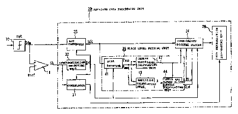
Next, the received data processing unit 23 will be dr3sCribed with
re~exence to Fig. 2. Tae received data processing unit 23 of the
n~asent invention inclsdes at least a correlator 3' to which the binary
signal. Sb from the comparator 11 of the reception circuit 3 is input and
which detects the synchronization word part SW in the access Code part
RC; a synchronization detecting unit 32 to which the binary signal Sb is
input and which serves as synchronization establishing means for
establishing synchronization with a 01 pattern of the preamble part FA
so as to output a synchronization signal SY: an R/D corv$rter 33 for
A/D-converting the analog demodulation signal Sda input from the
detection ci.xCUit 10 of the reception circuit 3 bused on the
synchronization signal SY output from the synchronization detecting unit
32 so as to generate a digital demodulation signal Sdd; ~ four-valued
digital slicer 39 for slicing the digital demodulation signal Sdd output
from the A/D converter 33 when a correlation signal is output from the
correlator 31 by using three slice level reference values so as to
generate a tour-valued digital signal; a slice level setting unit 35
CA 02411742 2002-11-13
- 16-
servirg as reference value correcting t~:eans fox setting the slice level
reference values used i.r. the digital sliver 34: and a data reproduction
processing ur_it 36 to which a four-valued digital signal output from the
digital sliver 39 is input.
[0026]
'.'he slice level settir_g unit 3S includes a peak detector 91 for
detecting a minimum peak Pmin and a maximu.-n peak Prnax corresponding ~o
40 and 10 of a four-valu~~i FSK of the digital demodulation signal Sdd
auCput from the A/D convette= 33 when the synchronization signal SY is
output from the synchronization detecting unit 32: a center slice level
calculating unit 92 fox Calculating a cent~az value 5Lc of the slice
level based on the minimum peak Pmin and the maximum peak Pmax detected
by the peak detector 41; an amplitude calculating unit 93 ~or
calculating ari amplitude A of the digital rcCept~.ori signal based on the
minimum peak Pmin and the maximum peak Pmax detected by the Peak
detector 41; and an upper and lower slice le~dels calculating unit 49 for
calculating upper arid lower slice levels SLu and STrd sahdwiching the
Center voice SLc by adding/subtracting 1/3 of the amplitude A obtained
in the amplitude calcu:.ating unit 43 to/itom the center value ST_.c
obtained in the Center slice level Caloulating unit 42. The Center
slice level SLe obte~iried in the center slice level calculating unit 42
and the upper and lower slice levels sLu and SLd obtained in the upper
and lower slice levels calculaCing unit 49 are input as slice level
reference values to the four -valuod digital sliver 39.
[0027]
CA 02411742 2002-11-13
j7_
The transmission circuit 4, the frequency synthesizer 15, the
CransT,ission data processing unit 21, and the frequency topping control
unit 22 form transmittxny means.
NFxt, the operation of the above-described embodiment will be
described.
A packet, in v.=hick the access code part Ac and the header part FD
are formed by 00 and 1G and the payload pert PL is a four-valued F5K
modulated by using 00, Ol, 17., and 10, is transmitted from a short-range
radio communication apparatus having the same co7Figuration as "hat of
the short-range radio communiaat_on apparatus tdC shown in Fiq. I to the
short-range radio communication apparatus WC, while frequency hopping is
performed in a frequency band in the range of 2.900 GHz to 2.980 GHz.
Tre packet is received by she Ctansmitting/rece::ving antenna 1 of Che
short-range radio corrununication apparatus ~~1C.
[0028)
A rQCeption signal received by the transmitting/receiving antenna 1
is supplied to the reception circuit 3 through the
trarismission/reception switching circuit 2.
In tl:e reception circu~,t 3, the reception signal is supplied to the
band-pass filter 5, the Zilter 5 extracts only a necessary band, the
extracted component of the teceptien si.gn,~l is amplified by the 1ow-
noise amplifier 6, is mixed with the local oscillation output LO of the
voltage-co:~trolled oscillator 19 in the mixer 7, and is converted to an
intermediate-frequency signal IF. Then, the intermediate-frequency
signal TF is supplied to the band-ps~ss filter 8 so as to remove an image
CA 02411742 2002-11-13
' -18-
signal generated at the mixing, is amplified iri the limiter amplifier 9,
and is supplied to the detection circuit Ø A detected analog
demodulation signal Sda is directly znput to the received data
processing unit 23 of the baseband signa'_ processor 12 and a binary
signal Sb generated by slicing and biriarizing the analog demodulation
signal Sda in the comparator 11 is also input to the received data
processing unit 23 of the basebarid signal processor 12.
(0020
In the received data processing uni" 23, the synchronization
detecting unit 32 establishes synchxoni2ation based on the binary signal
Sb correspardi,ng to the preamble part PA of the O1 pattern and the
synchronization word part STro. Then, a=ter synchronization has been
established, a synchronization signal SY 1s output to the A/D converter
33 arid to the peak detector 41 of the slice level setting unit 35.
The A/D converter 33 converts the analog demodulation signa~i Sda to
a digital signal at the timing of indication of the synchronization
signal SY. T~7h~r. the digital signal is input to the slice level setting
unit 35, the peak detector 91 detects the minimum peak Pmin arid the
maximum peak Pmax corresponding to 00 and 10 of the spur-valued FS1S of
the synchronization word part SW. The minimum peat pmin and the maximum
peak Pmax a=E Supplied to the center slice level oalculati~ag unit 42,
where an average is calculated so as to obtain a center slice level SLc.
On th4 other hand, the amplitude calculating unit 93 calculates the
amplitude A, which is supplied to the upper and lower slice levels
calculating unit 44. The upper and lower slice levels calculating unit
CA 02411742 2002-11-13
_ ly _
44 calculates the upper a;~a lower slice leve:.s SLu and SLd sandwiching
~~he center slice level Sic based on tho amplitude A and the center slice
level SLc. Tze Cen2et slice level. SLC and the uppex and =ower slice
levels SLu and SLd are suppl:.ed to the four-valued digital sliter 34.
[0030)
On the otter hand, it the c:orrelator 37., a shift reg.i.ster
sequentially reads data, which is set in the synchronization word dart
Stv and which is used tox identifying the packet, in acco=dance with the
sy:uChronizatvon signaW SY. Also, the Correlator 31 calculates the
correlation between the data and an identification word Set in advarce.
When tl:e correlation value reaches its peak and the data matches the
identification ~.:ord, a correlation signal :~s output to the data
reproduction processing unit 36.
The tour-valued dig:.ta1 slicer 39 compares the d~,gital demodulation
signal Sdd corresponding to the payload part PL with the referents
values, that i_, the center slice level SLc and the uppet and lower
slice 'revels SLu and SLd set in the slice level, setting unit 35, and
converts the digital demodulation signal 5dd to four digital values: 00,
O1, 1;" and 10. The digital values axe output to the data repxaduGtion
processing unit 36 so that the transmission data is reproduced.
(0031]
As described above, according to the embodiment, the transmitter
side transmits a packet, in which the access code part AC including the
preamble part PA arid the synchxoni2ation wozd part SW and tht header
part HD are formed by binary of 00 and 10 indicating the minimum valu~
CA 02411742 2002-11-13
and the maximum value in the dour-valued :SK acid in which the payload
part PT~ is formed by øour values of 00, O1, 11, and 10, by FSK
r~odulatioz. Accordingly. the receivex side, that is, t:~~e short-range
radio communication apparatus i~lC, receives the packet. and tl:e analog
demodulation signal Sda detected by the detection circuit l0.and the
binary signal Sb generated by b:.narizing the analog demodula:ion signal
Sda in the compatator 11 are supplied to the received data processing
unit 23 of the baseband signal processor 12. Accordingly, in the
received data processing unit 23, synchronization can be established arid
coxxelation of the synchronization word part can be achieved based on
the binary signal Sb. Tn a state that the synchronization is
establishes, the slice level, :,etting unit 35 calculates she slice level.
reference values so as to perform correction. Thus, th_~ sampling period
of the A/D ooriverter 33 can be lowered and a hardware configuration fox
calculat~,ng the slice level can be simpJ.ifi.ed.
f,0032~
Further, both of the analog demodulation signa]. Sda and the binary
signal Sb are input to the received data processing unit 23 c' the
baseband signal processor 12. Thus, when a packet in which the entzra
packet is binary FSK modulated is received, both of the signa7.s are
detected from the header part HD. zri this case, whet. correlation is
detected in the Correlator 37., the A/D converter 33 can be Stopped arid
the binary signal output fxom the comparator I1 can be directly supplied
to the data reproduction processing unit 36 so as to be reproduced.
Also, the power consumption in the A/D Converter 33 can be significantly
CA 02411742 2002-11-13
?1
reduced, and the power consumption when a alnary FSK modulated pac'.tet is
received car. be significantly reduced compared to when a four-valued FSK
modulated packet is =eceived.
[0033]
In the above-described embodiment, sync:~rOnization and calculation
of the slice level reference values axa performed in the period of the
preamble port PA and the synchronization word part 5W of a packet.
However, the present invention is not limited thereto. Alternat'_vcly,
as shown in Fig. 5, the transmitter lice can form a packet iri which an
auxiliary synchronization signal part 5S, which is formed by QO and 10
indicating the mini_nLm value and the maximum vague in the fou,C-valued
FSK as in the preamble part PA, is inserted into the payload part PL
with a predetermined time interval from the start point of the payload
part PL subsequent tc the access code part AC. Aiso, the received data
processing unit 23 0! the baseband signal processor 12 in the receiver
side aerforms a synchronization establishment pzocess '_llusttated :.n Fig.
6. In the synchronization establishment process, it is determined
whether or not a correlation signal is .input from the co;relator 3'_ in
step 5:.. If the correlation signal is not inpuC, it is detezmined that
no packet is recej.ved arid ~he process waits until a correlation signal
is input. When a correlation signal is input, the process proceeds to
step 52, wha:e d timer which is counted up in a predeCermined time is
started. Then, in step 53, it is determined whether or not the timer is
counted up, If the timer is riot counted up, the process proceeds to
step S4 so as to dete:mina whether or not a payload part PI. exists. bf
CA 02411742 2002-11-13
- 2? -
a payload part PL does not exist, it is determined that the reception of
the packet is completed and the pzocess ~eturn5 to step S,. It a
payload part PT. exists, it is determined that a packet is being received
and the process returns to step S3. on the other hand, if the timer is
counted up in sCep S3, the process proceeds to step S5, where the
synchronization detecting unit 32 and the Slice level setting unit 35
are operated for a time ir_ which the auxiliary syncrjroriization signal
part SS is processed so a~ to establish synchronization and .se~ the
slice level again. Then, the process ~etutns to step S2.
[0034]
The process shown in Fig. 6 corresponds to auxiliary
synchronization signal position d~tectiag means.
Therefore, by establishing synchzona,zation and setting the slice
level ovary time the auxiliary synchronization signal part SS included
7.n the payload part Ph of a packet is detected, stagger of
synchronization and slice level caused when the number of bits of the
payload part P~, is large can be reliably prevented.
[0035)
In the above-described eirbodiment, the slice level setting unit
sets the center slice level Sc and positive and negative slice levels Sp
and Sn based on the digital reception signal o4tput from the A/D
converter 33. Alternatively, the center level of the digital reception
signal output from the A/D converter 33 is corrected in accordance with
the center slice level sLc obtained in the center slice level
calculating unit 92 so that the signal is supplied to the four-valued
CA 02411742 2002-11-13
33 -
digital slicer 39.
(003'v]
Further, in the abev4-described embodiment, tour-valued FSK
modulation/demodulatien is described. However, the present invention
can be applied when multi-valued FSK communiCaeion is performed, for
example, eight-valued FSK modulation/demodulation.
Ir_ addit:.on, in the above-described embodiment, the present
invention is applied to a short-range radio communication apparatus
using an ISM band. Altaxl:atively, the present invention can be applied
to another Cype of radio communiodtion apparatus, yor example, radio LR'H
using another band.
[0037]
[Advantages]
As dasCribed above, according to the invention of Claim 1 Or A, the
transmitter side forms the transmission signal by performing ttiulti,
valued FSK modulation using only the minimum value and the maximum value
in multi-valued F9K ~a,t:~ respect to the synchronization signal part o~
the packet and by peryormi,i~g normal multi-valued F5K moduJ.ation with
respect to Lhe payload part, and transmits the transmission signal to
the receiver side. The receiver side outputs the analog demodulation
signal and a binaxy sicnal generated by binarizing the analog
demodulation signal from a. recnsption circuit unit for demodulating the
reception signal to a baseband processing vnj,t. Also, in the baseband
processing unit, the re=erence value for determining the'level o~ multi-
valued FSK based on the digital demodulation signal generated by A/D-
CA 02411742 2002-11-13
converting the anawog demodulation signal aftet synchronization ;s
established based on the binary signal is corrected, and then the
payload pare o.f the analog demodulation signal is A/D-converted so as to
be compared wi:.h the reference value, and the multi-valued digital
signs; is gsaerated. Therefore, establwshma:tt of synchronization of the
received packet and correction, of the reference value can be easily
performed with a simple conf:.guratiori.
[0038]
Also, the binary signal is generated from the analog demodulation
signal in the reception circuit unit and the binary signal is supplied
to the baseband processing unit. Thus, a packet of a multi-valued FSK
can be reproduced by using the A/D Ccnverter and a packet of a binary
FSK can be reproduced based on the binary signal without using the A/D
converter. Accordingly, po'rier can be saved.
[00391
Also, according to the invention of Cla~.n: Z or S, when the frame of
the payload part of the packet is long, the transmitter side inserts an
auxiliary synchronization signal part corresponding to the
synchronization signal part into the payload part with an interval of
predet~rmined time from the end of the synchronization signal part, the
baseband processing unit in the receivet side measures the predetermined
time f=om the end of the synchronization signal part, synchronization is
established based on the binary signal output from the reception circuit
unit every time the predetermined time passes, and the reference value
is corrected. Thus, stagger of synchronization and reference value can
CA 02411742 2002-11-13
_ 7j _
be reliably prevented even when the frame of the payload part of a
packet is long, Ir this case. special hardware used for integratirig and
avetdging the reference va'ue, which is required in Ghe first known art,
is unnecessary. Rccozdingly, the size and cast of the device can be
reduced and low power consumption car. bo realized.
[0040
Further, dccOtding to the invention of Claim 3 or 6, a large error
is not caused when the reference value in the fouY-valued FSK is
corzected, and thus the refazence value can be stably corrected.
(Brie; pescription of the D;awingsj
F'ig. ], is a block diagram showing an embod~,merit of the pxQSont
invention.
F~,g. 2 is a block diagxara showing a specific configuration of a
received data processing unit 23 shown in Fig, 1.
Fig. 3 shows an example of a pac:tet.
Fig. 4 shows a fouz-valued FSK signal of the packet.
Fig. 5 shows a modification of the packet.
Eig. 6 is a flowchart showing an example of a process of
establishing synchronization.
CA 02411742 2002-11-13
,.
Fig. 7 is a block d:.agram showing a known synchronization
esLablisk:ment circuit.
Fig. 8 is a block diagram showing anothas known synchronization
establi.shmer.t circuit.
[Reference Numerals?
WC: short--range =adio communication apparatus
1: antenna
2: transmission/reception switching circuit
3: reception circuit
4: trans:::ission circuit
10: detection circuit
1.: co:nuarator
12: baseband signal p~otessor
15: Frequency synthesizer
21: traasmissien data processing unit
22: frequency hopping control unit
23: received data processing unit
31: correlator
32: synchroY:ization detecting unit
33: ,A/D converter
34: four-valued digitatl slicer
35: slice level setting unit
36: data repxoduCtiori processing unit
CA 02411742 2002-11-13
_7
41: peak deteccot
42: center slice level calculating unit
A3: amplitude calcula.tirig Gr.;t
44: upper arid lager slice ravels calculating unit