Note: Descriptions are shown in the official language in which they were submitted.
CA 02412194 2002-12-06
WO 01/96922 PCT/USO1/18497
TITLE
MEMS DEVICE HAVING MULTIPLE DWDM FILTERS
CROSS-REFERENCE TO RELATED APPLICATION
[001] This application claims priority to Provisional Patent Application
Number
60/210,52, filed on June 9, 2000.
FIELD OF THE INVENTION
[002] The present invention is directed to an optical
multiplexerldemultiplexer for
use with an optical input signal which can consist of several different
wavelength division
multiplexing ("WDM") or dense wavelength division multiplexing ("DWDM")
channels. In
the case of a demultiplexer, the optical filter can pick off one of these
different
WDM/DWDM channels allowing the demultiplexer to be "tuned" in a step-wise
manner to
extract the desired channel from the multichannel input signal. The optical
channel of
interest can be separated from the optical input path along an output path,
and the remaining
channels of the multichannel input signal remain available for use.
BACKGROUND OF THE INVENTION
[003] Optical fibers play an important part in the transmission of digital
data, since
such optical fibers can transmit large amounts of data rapidly. Although early
optical fibers
were used to transmit just a single wavelength of light, the ever-increasing
need to increase
optical fiber bandwidth has led to optical data transmission systems which
transmit multiple
wavelengths of light through a single fiber (bandwidth is a term of art and
refers generally to
the amount of data which a signal path can carry).
CA 02412194 2002-12-06
WO 01/96922 PCT/USO1/18497
2
[004] The terms "light signal" and optical signal" as used herein are
interchangeable
and are intended to be broadly construed and to refer to visible, infrared,
ultraviolet light, and
the like which fall within the transparency region of the optical fiber.
[00S] Among the ways in which optical fiber bandwidth has been increased is
through the use of wavelength division multiplexing ("WDM"), along with the
related
technique of dense wavelength division multiplexing ("DWDM"). WDM and DWDM
allow
a single optical fiber to carry more than one wavelength of light; each
wavelength of light
sent through the optical fiber corresponds to a single channel of data.
Increasing the number
of channels which an optical fiber can support increases bandwidth
accordingly; doubling the
number of channels doubles the bandwidth. The channels of a WDM or DWDM system
are
separated in wavelength by some minimum spacing to avoid interference effects
which might
occur between the signals in adjacent channels. Presently, 100 GHz of optical
frequency
spacing, corresponding to approximately 0.8 nm spacing between adj acent
optical channels is
common, although in advanced systems spacings of SO GHz are being deployed.
[006] Both WDM and DWDM employ multiplexers and demultiplexers combine
and separate, respectively, channels from multichannel optical signals. As
depicted in FIG. l,
a multiplexer 3 receives several input optical signals A, B, C, D and E, each
at an associated
wavelength, via inputs 1, 1', 1 ", 1"' and 1"", respectively. The multiplexer
3 combines
optical signals A, B, C, D and E and outputs those signals to optical fiber S.
This way, each
of optical signals A, B, C, D and E are simultaneously transmitted through the
same optical
fiber S.
[007] Optical fiber S leads, either directly or indirectly, via other signal
lines, to
demultiplexer 7. Demultiplexer 7 takes the combined optical signal from
optical fiber S and
separates that combined optical signal into output signals A', B', C', D' and
E', which are
available on outputs 9, 9', 9", 9"' and 9" ", respectively.
CA 02412194 2002-12-06
WO 01/96922 PCT/USO1/18497
3
[008] It will be appreciated that demultiplexer 7 is the functional opposite
of
multiplexer 5. The former separates channels from a multichannel signal, and
the latter
combines separate channels to obtain a rnultichannel signal.
[009] In prior art tunable filters multiple wavelengths come in on a single
fiber, the
chosen dropped wavelength emerges on a separate fiber, and the remaining
wavelengths
leave together on a second output fiber. The filter, being tunable, can
be~adjusted to pick out
any one of the input wavelengths.
[0010] Prior art tunable filter devices include tunable Fabry-Perot
interferometers,
liquid crystal filters, temperature tuned fiber Bragg gratings and unbalanced
Mach-Zehnder
interferometers.
[0011] A common aspect of such known tunable filters is that they tune
continuously,
not discretely, and hence require some sort of external wavelength
calibration.
[0012] Size is an ever-present concern in the design, fabrication, and
construction of
optical components (i.e., devices, circuits, and systems), including
multiplexers and
demultiplexers. It is clearly desirable to provide smaller optical components
so that optical
devices, circuits, and systems may be fabricated more densely, consume less
power, and
operate more rapidly and more efficiently.
[0013] There is an ever-increasing need to transmit more and more data over
optical
signal paths. There is a corresponding need for improved multiplexers and
demultiplexers
which are small in size, fast in their multiplexing, and reliable in
operation.
SUMMARY OF THE INVENTION
[0014] The present invention is directed to an optical signal processing
method and a
device which can serve as a signal multiplexer or demultiplexer. This device
has a movable
filter assembly having a number of filters, with each filter having a surface
which reflects a
CA 02412194 2002-12-06
WO 01/96922 PCT/USO1/18497
4
particular wavelength of light and passes other wavelengths of light. This
defines two
wavelength-dependent signal paths. Light reflecting from a reflective surface
of the filter
passes along one signal path which includes an input waveguide and a first
output waveguide.
Light transmitted through the alter travels along another signal path which
includes the input
waveguide and a second output waveguide. The filter can be contained in a
trench separating
the input and second output waveguides, and can be moved in the trench to
alter the optical
properties of the two signal paths.
[0015] Both multiplexers and demultiplexers can be constructed in accordance
with
this invention according to the direction in which light travels.
[0016] Among the benefits of this invention is that unlike known continuously-
tunable filters, this invention provides for discrete alter tuning steps.
Tuning is effected
stepwise in discrete amounts that correspond exactly to the DWDM wavelength
spacings
specified by the ITU grid. In contrast to known devices, external wavelength
calibration is
not required.
[0017] A further benefit of this invention is that the tunable filter device
is, owing to
its manner of construct, readily integrated with other planar waveguide
devices such as
splitters, taps, couplers and switches. By virtue of this invention high
performance photonic
integrated circuits (PICs) can be made which incorporate wavelength filtering
as one of the
functions that they can perform. This is a distinct advantage over known
tunable filters such
as Fabry-Perot, liquid crystal and temperature tuned fiber Bragg grating
devices.
[0018] In addition, an optical signal processing device in accordance with the
present
invention can have a first waveguide separated by a trench from both a second
waveguide
coaxial with the first waveguide and a third waveguide oriented at an angle to
the first
waveguide. A filter assembly having reflective filters each reflecting only a
particular
wavelength of light is movably positioned in the trench, and an actuator
connected to the
CA 02412194 2002-12-06
WO 01/96922 PCT/USO1/18497
filter assembly moves the assembly so that a particular filter is positioned
between the first
and the second waveguides. This way, an optical signal propagating in and
along the first
waveguide which has a wavelength approximately equal to the reflective
wavelength of the
filtex between the first and the second waveguides is reflected from the
filter into the third
waveguide, whereas an optical signal not having a such a wavelength is
transmitted through
the filter assembly to the second waveguide.
[0019] Another aspect of this invention involves a method of processing a
multichannel optical signal by reflecting one channel from a reflector into a
first output
waveguide and transmitting the other optical channels through the reflector
into a second
output waveguide.
[0020] Still another aspect of this invention relates to limiting an angle of
incidence at
which the optical signal strikes the reflector's front surface to be not more
than approximately
I O°. This may be preferable in order to achieve polarization
insensitivity.
[0021] The invention accordingly comprises the features of construction,
combination
of elements, and arrangement of parts which will be exemplified in the
disclosure herein.
The scope of the invention will be indicated in the claims.
BRIEF DESCRIPTION OF THE DRAWINGS
[0022] In the drawing figures, which are not to scale, and which are merely
illustrative, and wherein like reference characters denote similar elements
throughout the
several views:
[0023] FIG. 1 is a schematic view of a prior system for transmitting multiple
channels
of optical data over a single optical fiber; '
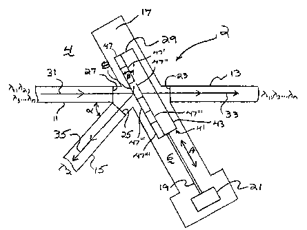
[0024] FIG. 2 is a top plan view of a MEMS device having multiple DWDM filters
in
accordance with a first embodiment of the present invention;
CA 02412194 2002-12-06
WO 01/96922 PCT/USO1/18497
[0025] FIG. 3 is a perspective view of a filter assembly of the device
depicted in FIG.
2;
[0026] FIG. 4 is a perspective view of the filter assembly shown in FIG. 3;
[0027] FIG. 5 is a perspective view of a second embodiment of a filter
assembly in
accordance with the present invention; and
[0028] FIG. 6 is a perspective view of a third embodiment of a filter assembly
in
accordance with the pxesentinvention.
DETAILED DESCRIPTION OF THE PRESENTLY PREFERRED EMBODIMENTS
[0029] The present invention is directed to an optical device having an input
waveguide and two output waveguides separated by and disposed around a trench.
The input
waveguide and a first output waveguide have respective optical paths defined
by their
respective cores, and those optical paths (and cores) are aligned or coaxial
with each other.
Typical channel waveguide cross-sectional dimensions are 7 ~,m by 7 p.m. The
waveguides
are separated by the trench, the trench having a medium provided therein that
has a refractive
index different from that of the waveguides. A movable filter assembly is
disposed in the
trench in such a way that the filter assembly.can be shifted into and within
the optical path
(i.e., of light leaving the input waveguide). The filter assembly is
constructed so that
different portions of the filter will reflect different wavelengths of light.
Consequently, the
position of the filter assembly in the trench will determine the wavelength of
light passing
from the input waveguide to the first output or dropped channel waveguide, as
well as the
wavelengths of light which are transmitted through the filter assembly to the
second output or
through channel waveguide.
[0030] Moreover, the input waveguide and through channel waveguide axe
separated
by a distance insufficient to significantly affect the transmission
characteristics of an optical
CA 02412194 2002-12-06
WO 01/96922 PCT/USO1/18497
7
signal propagating from the input waveguide, through and across the trench and
to the
through channel waveguide, even though the optical signal experiences
different refractive
indices as it propagates from the input waveguide through the filter (and
trench) to the
through channel waveguide. Thus, even though the optical signal experiences
some
diffraction as it propagates across the trench and may pass through the
filter, the distance over
which the optical signal must pass between the waveguides is small enough so
as to not to
significantly affect the optical transmission characteristics of that signal.
Excess loss will be
less than 10 dB.
(0031] In like manner the input waveguide and the dropped channel waveguide
are
arranged generally on the same side of the trench such that an optical signal
passing from the
input waveguide to the dropped cham~,el waveguide does not completely traverse
the trench
but instead, reflects off the surface of a filter. Once again, even though the
optical signal
experiences different indices of refraction for the waveguide and medium
provided in the
trench, the optical signal propagates over a distance too small to adversely
affect the optical
transmission characteristics of that signal.
[0032] That is, while the trench is large enough to allow for the finite
thickness of the
filter assembly to be placed inside the trench, the trench should also be as
small as possible to
minimize the light diffraction in the trench gap.
[0033] Referring now to the drawings in detail, and with initial reference to
FIG. 2, a
demultiplexer 2 constructed in accordance with an embodiment of the present
invention is
there depicted. The waveguide construction described below is provided as an
illustrative,
non-limiting example of an embodiment of the present invention; other
waveguide
geometries and configurations are contemplated by and fall within the scope
and spirit of the
present invention.
CA 02412194 2002-12-06
WO 01/96922 PCT/USO1/18497
8
[0034] The demultiplexer 2 includes an input waveguide 11, a through channel
waveguide 13, and a dropped channel waveguide 15 arranged around trench 17
such that
input waveguide 11 and through channel waveguide 13 are separated by the
trench 17. Input
waveguide 11 and the through and dropped channel waveguides 13 and 15 can be
constructed
in accordance with the general knowledge in the art. By way of non-limiting
example, the
waveguides 11, 13 and 15 can be constructed using semiconductor fabrication
techniques
such as reactive ion etching and methods known to those skilled in the art,
and thus need not
be described in detail here. At present it is thought that a buried waveguide
con ~guration is
preferable. Further, waveguides 11, 13 and 15 could be formed from a wide
variety of
materials chosen to provide the desired optical properties. By way of further
non-limiting
example, it is believed preferable to construct the demultiplexer 2 of the
present invention
using a waveguide structure that supports large optical mode sizes that
minimize the
diffraction losses crossing the trench. Preferred examples are silica based.
For example,
germanium-doped silica would be used for the channel waveguides and thermal
Si02 or boron
phosphide-doped silica glass could be used for the cladding layers.
[0035] As explained in greater detail below, an optical signal 31 propagating
in and
along input waveguide 11 is a multichamlel signal having a plurality of
wavelengths ~,1, 7~z, ~3
. . . ai, (n is an integer). The optical signal 35 propagating in and along
dropped channel
waveguide 15 is a single-wavelength signal corresponding, for the purpose of
illustration
only, to wavelength ~,Z (other wavelengths also could be dropped). All of the
other channels
(i.e., wavelengths) of the optical signal 31 propagate across trench 17
through alter assembly
41 into the through channel waveguide 13 as signal 33, which consists of
wavelengths ~.1, 7~3 .
. . a," (n is an integer). Changing which channel (i.e., wavelength) is
directed through the
dropped channel waveguide 15 will change which channels (i.e., wavelengths) of
optical
CA 02412194 2002-12-06
WO 01/96922 PCT/USO1/18497
9
signals are transmitted along the through channel waveguide 13. As used
herein, the terms
"channel" and "wavelength" are generally interchangeable.
[0036] With continued reference to FIG. 2, it will be noted that the optical
signal 31
traveling in and along input waveguide 11 leaves the waveguide 11 through
output facet 27,
(the term "facet" refers to an end of a waveguide) and enters trench 17. The
optical signal 31
continues onward across the trench and strikes filter assembly 41.
[0037] As depicted in FIGS. 2 and 3, filter assembly 41 has a number of
filters 47,
47', 47", 47"', 47"" mounted on support 45. Each filter 47, 47', 47", 47"',
47""
corresponds to a particular signal channel; that is, each filter reflects a
different wavelength
of light 7~1, 7~2, ~.3 . . . a,1,. A back support 43 is positioned on support
45 behind and in abutting
contact with filters 47, 47', 47", 47"' and 47"". Preferably, the filters 47,
47', 47", 47"'
and 47"" and the back support 43 are joined to both each other and the support
45 by a
suitable bonding technique such as UV adhesive. Thus, the back support 43
stiffens and
strengthens filter assembly 41.
[0038] It is thought to be preferable to use vacuum deposited dielectric
staclcs as the
filter structure, this, being a generally well-known way of producing high-
resolution filters.
Such filters are able to resolve the DWDM channels. Deposition of the films
could be made
directly onto the support and be patterned lithographically.
[0039] Although as depicted in FIG. 2, filters 47-47"" are directly adjacent
to one
another, those filters need not be directly next to each other. Adjacent
filters could be
separated by islands of non-reflective material (not shown). Alternatively,
the filters could be
separated by sensor regions, which would indicate when those sensor regions
are struck by
the input optical signal 31. Such sensors could thereby help monitor the
position of the filter
assembly 41 along trench 17.
CA 02412194 2002-12-06
WO 01/96922 PCT/USO1/18497
[0040] Support 45 is preferably made from a light yet stiff material such as
silicon,
polymers, metallic or dielectric materials commonly used in MEMS technology.
Such a Iow-
mass, rigid support 45 can be caused to move quickly in response to an
electrical signal, fox
example, between the position depicted in FIG. 2, in which the optical signal
31 output from
the input waveguide 11 strikes filter 47" so that a portion 35 of that optical
signal 31 is
reflected from the front surface 8 of filter 47" to the dropped channel
waveguide 15 and the
remainder of the optical signal 31 travels as optical signal 33 through filter
47" and in and
along the through channel waveguide 13, and other positions (not shown) in
which other
filters 47, 47', 47"', 47"" lie in the path of the optical signal 31 or even
shift the filter
assembly 41 so that no filter lies in the path of optical signal 31.
[0041] Back support 43 is preferably transparent to all wavelengths, meaning
that an
optical signal having one or a plurality of wavelengths can pass therethrough
without
attenuation. As shown in FIG. 2, optical signal 33 emerges from back support
43, and passes
through input facet 23 into through chamlel waveguide 13.
[0042] With reference now to FIG. 4, filter 47"" is depicted in detail. It
should be
noted that the following detailed description of filter 47"" is illustrative
of each filter of the
filter assembly 41. The detailed discussion of filter 47"" thus applies
equally to each filter
of the filter assembly 41, unless expressly stated to the contrary. As shown
in FIG. 4, filter
47"" has a height hf, a width wf and a thickness tf and is mounted upon
support 45, which
has a thickness is and a height hs. Filter 47"" is composed of a stack of
dielectric thin films
10 having an overall thickness t~. The back support 43 has a thickness tv, and
a height by
which can be the same as hf. By way of non-limiting example, these dimensions
could be
selected as follows: hf= 10-25 pm, wf= 15-35 E~m, tf= 0.5-5 p.m, is = 8-15
lun, hs = 50-500
pm, t~ = 0.1-2 pm, tb = 3-7 ~.m, and hb = 10-25 ~,m.
CA 02412194 2002-12-06
WO 01/96922 PCT/USO1/18497
11
[0043] By way of non-limiting example, since the diameter of the beam of the
input
signal 31 in the trench 17 is approximately 10 ~.m, the minimum height hf and
width wf of
each filter 47, 47', 47", 47"', 47"" is preferably approximately 20 ~.m. This
way, optical
signal 31 will be fully-intercepted by each filter 47, 47', 47", 47"', 47"".
[0044] More particularly, a tunable filter in accordance with this invention
could be
constructed such that each filter is approximately 20 ~.rn wide and
approximately 20 ~.m high.
The entire filter assembly could be about 200 pm wide and approximately 40 ~,m
high.
[0045] Furthermore, the first and the second waveguides could be separated
from
each other by a distance of not more than approximately 8-40 Vim, and more
preferably, not
more than approximately 12-20 Vim.
[0046] Given the foregoing filter dimensions, and for a linear displacement of
the
filter assembly 41 of approximately 200 ~,m, the filter assembly 41 may be
constructed with
ten filters for filtering ten DWDM channels (for convenience, not all ten
filters have been
depicted). It is thought to be preferable to minimize the size of the filter
assembly 41 in order
to reduce the electrical power required to move the filter assembly 41 along
the optical path,
and improve the speed with which the demultiplexer 2 can be switched between
channels.
[0047] The major effect of the filter/back support thickness is a lateral
translation of
the transmitted beam, although the beam will still propagate parallel to its
original direction.
This translation can be compensated for by laterally displacing waveguide 13.
[0048] Filters 47, 47', 47", 47"' and 47"" have differing optical properties
such that
different wavelength optical signals reflect therefrom, and other, non-
reflected wavelengths
of a multi-wavelength optical signal can pass therethrough without substantial
attenuation.
The reflective material 10 coating each filter 47, 47', 47", 47"', 47"" has a
thickness or
composition selected such that a particular wavelength optical signal can be
reflected
therefrom, and so each of filters 47, 47', 47", 47"' and 47"' reflects a
particular wavelength
CA 02412194 2002-12-06
WO 01/96922 PCT/USO1/18497
12
of the optical signal 31 ox channel of data. Accordingly, the position of
filter assembly 41
will determine the optical signal channel which will be reflected by the
reflective material 10.
[0049] As noted above, the composition and thickness of the reflective
material 10
applied to the face 8 of each filter 47-47"" will determine the wavelength of
light that will
be reflected.
[0050] Each of filters 47, 47', 47", 47'", 47"' could be made to reflect a
particular
wavelength of light ~,1, 7~2, ~.3 . . . ?~" without attenuation and transmit
the remaining
wavelengths of light unimpeded using by forming a multilayer dielectric stack.
Tllis can be
accomplished using techniques which can be employed to fabricate thin-film
dielectric
interference filters. As this aspect of the fabrication technology is itself
known, no further
explanation of thin film fabrication techniques is needed.
[0051] Alternatively, each of filters 47, 47', 47", 47"', 47"' could be made
to reflect
a particular wavelength of light ~,1, ~2, ~3 . . . ~," by using filters made
from different materials.
Such filters would not have to be coated with a layer of reflective material.
By way of non-
limiting example, filters 47, 47', 47", 47"', 47"" could be made from Si base
material, with
each filter being doped with progressively more dopant, thereby changing the
optical
properties of the Si so that the Si is reflective (or alternatively,
transmissive) to different
wavelengths of light.
[0052] Referring back to FIG. 2, the dropped channel optical signal 35
propagates in
and along dropped channel waveguide 15, and can be directed to other devices
such as an
amplifier or opto-electrical converter (not shown) for further signal
processing.
[0053] With continued reference to FIG. 2, those channels of optical signal 31
which
are not reflected by the filter assembly 41 into dropped channel waveguide 15
(signal 35)
pass as signal 33 through input facet 23 into the through channel waveguide
13. Optical
signal 33 propagates in and along the through channel waveguide 13 for further
processing to
CA 02412194 2002-12-06
WO 01/96922 PCT/USO1/18497
13
other downstream devices such as additional demultiplexers (not shown), or the
signal can be
discarded.
[0054] Filter assembly 41 is contained in trench 17 formed in substrate 4 and
is joined
to actuator 21 by member 19. As shown in FIG. 2, actuator 21 can be driven to
cause filter
assembly 41 to reciprocate in the direction of arrow "A". By positioning.a
predetermined one
of filters 47, 47', 47", 47"' and 47"' in the path of optical signal 31, only
the wavelength to
which the predetermined filter is "tuned" will be reflected as beam 35 into
and propagate in
and along dropped channel waveguide 15; the remaining wavelengths pass through
the filter
as beam 33 and in and along through channel waveguide 13.
[0055] It also rnay be desirable to have the input optical signal 31 pass
directly and
without change into through channel waveguide 13. One way in which that can be
accomplished is by moving filter assembly 41 by a distance such that the
filter assembly 41
does not lie in the optical path between input waveguide 11 and dropped
channel waveguide
13.
[0056] Similarly, if it is desired to have all of the channels (i.e.,
wavelengths) of input
optical signal 31 enter dropped channel waveguide 15, one of filters 47, 47',
47", 47"' or
47"" or even a separate filter (not shown) could be coated with a material
which reflects all
of the wavelengths in the input optical signal 31. When such a mirrored filter
is moved into
the path of the input optical signal 31, the optical signal 31 will be
completely reflected into
the dropped channel waveguide 15.
[0057] With continued reference to FIG. 2, the optical paths defined by the
respective
cores of input waveguide 11 and through channel waveguide 13 are preferably
aligned or
coaxial with each other. This maximizes the amount of light transferred from
input
waveguide 11 to through channel waveguide 13.
CA 02412194 2002-12-06
WO 01/96922 PCT/USO1/18497
14
[0058] The dropped channel waveguide 15 defines an optical path that is
oriented
with respect to the input waveguide 11 optical path at a predetermined angle a
that is
preferably between approximately 5°-80°, and more preferably,
the angle between the
waveguides can be 16°.
[0059] Optionally, the facet 27 of the input waveguide 11 through which the
optical
signal 31 exits the input waveguide 11 to enter the trench 17, and the facets
23, 25 of the
through channel and dropped channel waveguides 13, 15, respectively, can be
angled with
respect to the corresponding waveguide's optical path (not shown). By way of
non-limiting
example, the angle of each of the facets could preferably be angled by between
approximately 6° and 10° relative to the optical axis of the
associated waveguide.
[0060] To improve optical properties, each facet is preferably provided with
an
antireflective (AR) coating. It is presently thought that the AR coating could
be on the order
of 0.5 ~m thick. Other relevant aspects of AR coating will be understood by
those skilled in
the art.
[0061] Trench 17 is defined in a substrate 4 (see, e.g., FIG. 2) that
separates the input
waveguide 11 and through channel waveguide 13, and around which the waveguides
are
arranged. The trench 17 is filled, partly or completely, with an optically
transparent medium
6 such as, for example, air, having an associated index of refraction n. For
air, the index of
refraction is approximately equal to 1.00.
[0062] By way of non-limiting example, the trench 17 could have a width wt of
approximately 8-40 pm wide, and more preferably, 12-20 pm wide.
[0063] With continued reference to FIG. 2, the actuator 21 causes the filter
assembly
41 to move reciprocally in the direction of arrow A. If desired, the actuator
21 could cause
the filter assembly to move in other directions as well, so long as that
movement provides the
ability to switch the particular filter 47, 47', 47", 47"', 47"" which is in
the optical path,
CA 02412194 2002-12-06
WO 01/96922 PCT/USO1/18497
and provided the actuator 21, member 19, trench 17 and other components are
suitably
arranged. By way of non-limiting example, the filter assembly could be moved
in a direction
perpendicular to the plane of the drawing.
[0064] Movement of the filter assembly 41 by the actuator 21 may be in
response to a
control signal input to the actuator 21 via an input (not shown). That contxol
signal may be
electrical, optical, mechanical, or virtually any other signal capable of
causing the actuator 21
to respond.
[0065] Various embodiments of the actuator 21 are contemplated by the present
invention including, by way of non-limiting example, electrothermal,
electrostatic, and
piezoelectric devices.
[0066] With reference now to FIG. 5, a second embodiment of the present
invention
is depicted, wherein filter assembly 141 is constructed such that the
individual alters 147,
147', 147", 147"' and 147"" mounted upon support 145 all have different
thiclcnesses tf.
For filters constructed of the same or optically equivalent material, the
wavelengths which are
reflected and which can pass through any of these filters 147, 147', 147",
147"' and 147""
are determined by the filter's thickness. Again, such filters are preferably
constructed using
thin-film dielectric interference filters, and those skilled in the art would
understand how to
prepare filters having the desired optical properties. Thus, instead of
changing the material
properties of the individual filters, or applying a coating thereto, or making
the filters from
different materials, to change the optical channels which each filter can
reflect/pass, the
filters 147, 147', 147", 147"' and 147"" are shaped so that their thicknesses
tf determine the
optical wavelength that can be transmitted.
[0067] It also will be appreciated that the filters 147 147', 147", 147"' and
147""
could be reversed to face back support 143. In that case, back support I43
could be provided
with a stepped surface matching the faces of filters 147, 147', 147", 147"'
and 147"", so
CA 02412194 2002-12-06
WO 01/96922 PCT/USO1/18497
16
that the stepped interface is located in between the back support 143 and the
filters 147, 147',
147", 147"' and 147"". Since back support I43 is optically transparent, the
fact that the
back support's thickness tb varies should not change the wavelength of the
optical signal
which can pass through the corresponding filter. In this arrangement, a
reflective coating (not
shown) or the use of differing filter materials for each filter 147, 147',
147", 147"', 147""
would be required.
[0068] A third embodiment of this invention, depicted in FIG. 6, contemplates
a filter
assembly 241 capable of two-dimensional movement. Filter assembly 241 includes
back
support 243, two rows of filters 247a-247a""' and 247b-247b""', and support
245. The
filter assembly 241 can be moved in the directions of both arrows A and B by a
suitable
actuators) (not shown). Consequently, the depth of the trench (not shown) in
which the filter
assembly 241 moves may have to be correspondingly modified. It will be
appreciated that
this arrangement can provide for a more compact and faster-operating device.
[0069] It also will be understood from this disclosure that by providing
additional
rows of filters (not shown), even more channels (wavelengths) of optical
signals can be
discriminated.
[0070] It should be understood that a 2 x 2 filter would be able to perform
both an add
and a drop of signals.
[0071] Those skilled in the art will in view of the foregoing disclosure
understand that
the present also encompasses filters which transmit the selected wavelength
and reflect all of
the other wavelengths. In such a filter the functions of the two output
waveguides 13, 15
would be interchanged.
[0072] Those skilled in the art will after reading the foregoing understand
that
although the disclosed embodiments are described as a demultiplexer 2, such
embodiments
are equally suited for use in a multiplexer through reversal of the direction
of propagation of
CA 02412194 2002-12-06
WO 01/96922 PCT/USO1/18497
17
the optical signals 31, 33, 35. By Way of non-limiting example, and with
reference to FIG. 2,
a single channel of optical information 35 propagating along waveguide 15
toward filter
assembly 41 could be combined with an optical signal 33 propagating along
waveguide 13
toward filter assembly 41. Optical signal 33 passes through back support 43
and filter 47" of
filter assembly 41, while optical signal 35 reflects off the front surface 8
of filter 47".
Optical signals 33 and 35 combine and propagate together along waveguide 11 as
multichannel optical signal 31.
[0073] To overcome the undesirable effects of the differing refractive indices
of the
different optical components used, the present invention controls the distance
between the
output facet 27 of the input waveguide 11 and the input facets 23, 25, of the
dropped channel
and through channel waveguides 13, 15 so that the optical signals 31, 33 and
35 propagate
over too short a distance for the difference in refractive indices to
introduce any significant
change in the optical signals' characteristics. Thus, even though the input
optical signal 31
completely traverses the trench 17 (from input waveguide 11 to through channel
waveguide
13), or partly traverses the trench 17 (from input waveguide 11 to dropped
channel
waveguide 15), the output optical signals 33 and 35 do not experience any
significant adverse
affect due to the difference in the medium 6 and waveguide respective
refractive indices.
[0074] In order to achieve polarization insensitivity, it may be preferable to
reduce
the angle of incidence (3 depicted in FIG. 2 of optical signal beam 31 onto
the filters' front
surfaces 8 to be not more than approximately 10°. It will be understood
that the angle of
incidence (3 refers to an amount by which the incoming optical signal beam 31
deviates from
the perpendicular to the plane of the front surface. Thus, a perpendicular
beam has an angle
of incidence of 0°. '
[0075] This invention can be manufactured using known fabrication techniques.
By
way of non-limiting example, these small spatially discreet DWDM filters could
be produced
CA 02412194 2002-12-06
WO 01/96922 PCT/USO1/18497
18
using photoresist patterning techniques such as etching through masking or
lift off
techniques.
[0076] The present invention will work with both weakly-confined waveguides
and
strongly-confined waveguides. Presently, weakly-confined waveguides are
thought to be
preferred.
[0077] Again, throughout the foregoing disclosure, the dimensions described
are
offered by way of example and not limitation. It should be understood that
this invention is
not intended to be limited to the angles, materials, shapes or sizes portrayed
herein, save to
the extent that such angles, materials, shapes or sizes are so limited by the
express language
of the claims.
[0078] While the present invention as depicted in FIG. 2 has a single input
optical
path 11 and two output optical paths 13, 15, ~it will be understood that
additional input and
output optical paths (not shown) could be included. By way of example, a
second input
waveguide and third and fourth output waveguides could be provided at a
different position.
[0079] Thus, while there have been shown and described and pointed out novel
features of the present invention as applied to preferred embodiments thereof,
it will be
understood that various omissions and substitutions and changes in the form
and details of the
disclosed invention may be made by those slcilled in the art without departing
fiom the spirit
of the invention. It is the intention, therefore, to be limited only as
indicated by the scope of
the claims appended hereto.
[0080] It is also to be understood that the following claims are intended to
cover all of
the generic and specific features of the invention herein described and all
statements of the
scope of the invention which, as a matter of language, might be said to fall
there between. In
particular, this invention should not be construed as being limited to the
dimensions,
proportions or arrangements disclosed herein.