Note: Descriptions are shown in the official language in which they were submitted.
CA 02412349 2009-11-06
- 1 -
Winding for a transformer or a coil
Description
The invention relates to a winding for a transformer or
a coil having a ribbon electrical conductor and having
an insulating material layer composed of ribbon
insulation material, which are wound jointly to form
turns around a winding core, with the individual turns
of the winding having a predetermined winding angle
with respect to the winding axis of the winding core,
and being arranged such that they partially overlap one
another, and with an insulating layer being inserted
between two radially adjacent layers of turns.
In generally known windings such as these, the turns
are normally wound such that they lie closely alongside
one another in the axial direction, and at least one
layer of turns is formed.
Frequently, however, a number of layers are also joined
to one another radially and form a multilayer
transformer or a multilayer coil. In situations where
there are a number of layers of turns an insulating
layer is in each case frequently introduced or inserted
between two adjacent layers. This insulating layer
prevents voltage flashovers between the layers, and is
accordingly designed for the maximum voltage difference
which can exist between two layers.
Against the background of this prior art, an object of
the invention is to specify a winding for a transformer
or a coil, in which insulation material can be saved
and in which, furthermore, an adequate withstand
voltage is achieved, and in particular a good impulse
withstand voltage between two radially adjacent layers
CA 02412349 2009-11-06
2 -
of turns.
The subject matter according to the invention is
therefore characterized in. that the local voltage
differences and/or a voltage difference profile between
the two relevant radially adjacent layers in the
direction of the winding axis are or is determined, and
in that the thickness of the insulating layer is
locally matched to the determined voltage difference in
each case. The insulating layer is therefore not
designed, as in the previously known prior art, with a
constant layer thickness, but the thickness is matched
to the voltage difference between the relevant radially
adjacent rows. It is therefore possible to save
insulation material at the axial points at which the
voltage difference is comparatively low. Furthermore,
this means that the transformer or the coil may have a
comparatively better impulse withstand voltage between
the layers, overall.
According to one aspect of the invention there is
provided a winding for a transformer or a coil having a
ribbon electrical conductor and having an insulating
material layer composed of ribbon insulation material,
which are wound jointly to form turns around a winding
core, with the individual turns of the winding having a
predetermined winding angle with respect to the winding
axis of the winding core, and being arranged such that
they partially overlap one another, and with an
insulating layer being inserted between two radially
adjacent layers of turns, wherein local voltage
difference and/or a voltage difference profile between
the two relevant radially adjacent layers in the
direction of the winding axis is determined, and
wherein the thickness of the insulating layer is
locally matched to the determined voltage difference in
each case.
CA 02412349 2009-11-06
- 2a -
One advantageous refinement. of the subject matter of
the invention, for an arrangement of two radially
adjacent insulating layers, is for the calculated
overall thickness of these two insulating layers to
have approximately the same thickness at every axial
point. This refinement advantageously results in the
different external diameters of a layer, which result
from the different insulating layer thicknesses, being
compensated for once again by means of the profile,
according to the invention, of a further insulating
layer between that layer and the next subsequent layer,
thus resulting' in the transformer or the coil having
the same external diameter overall.
CA 02412349 2002-11-21
01/623 - 3 - 21 November 2001
One advantageous refinement of the subject matter
according to the invention provides for the thickness
change in the insulating layer to be continuous in the
axial direction. This results in the insulating layer
having an approximately wedge-shaped profile, when seen
in the form of a section through the winding axis.
However, it is possible without any problems to provide
a sawtooth or corrugated profile in section, for
example, when two coils are arranged directly alongside
one another.
However, it is particularly advantageous for the
thickness change in the insulating layer to be in the
form of steps in the axial direction. This means that,
seen in the axial direction, the thickness of the
insulating layer changes suddenly in steps, that is to
say discontinuously, without this having any
disadvantageous effect on the withstand voltage.
Furthermore, this refinement means that the insulating
layer can be produced in a considerably simpler manner,
with the conventional ribbon insulation material being
wound layer-by-layer to form the insulating layer.
Further advantageous refinements of the invention are
specified in the dependent claims.
The invention, an advantageous refinement and
improvements of the invention, as well as particular
advantages of the invention, will be explained and
described in more detail with reference to an exemplary
embodiment, which is illustrated in the drawings, in
which:
Figure 1 shows a transformer winding with three layers
and
Figure 2 shows two mutually opposite insulating
layers.
CA 02412349 2002-11-21
01/623 - 4 - 21 November 2001
Figure 1 shows part of a three-layer winding for a
transformer. The winding is wound around a winding core
10, with a winding axis 12. The winding is formed from
a ribbon electrical conductor 1.4, which is coated with
a ribbon insulation material 16. As an alternative to
this, the ribbon insulation material 16 may also be in
the form of a r_Lbbon film. Furthermore, it is
irrelevant whether the electrical conductor 14 is
coated with the insulation material, or whether the
insulation material is formed as a ribbon in its own
right, together with the electrical conductor 14, to
form the winding.
That layer which is wound directly around the winding
core 10 will be referred to as the first layer 18 of
turns. The ribbon insulation material 16 is in this
case arranged such that it is located between the
winding core 10 and the conductor 14. The individual
turns of the first layer 18 are inclined through a
specific angle 20 with respect to the winding axis 12.
Furthermore, each turn is arranged offset by a specific
amount with respect to the previous winding, parallel
to the direction of the winding axis 12, such that a
next subsequent winding partially overlaps the
preceding turn. A second layer 22 of turns is wound
radially around the first layer 18. The winding
structure of the second layer 22 corresponds
essentially to the winding structure of the first layer
18, so that, in this case as well, the electrical
conductor 1.4 and the insulation material 16 are
designed such that they partially overlap, being
arranged turn-by-turn alongside one another. The axial
orientation of the overlaps of the first layer 18 and
of the second layer 22 is chosen such that they come to
rest at the same axial point on the winding axis 12.
The nature of the overlap in the second layer 22 is
chosen such that a winding angle 24 of the second layer
22 corresponds to the magnitude of the specific angle
CA 02412349 2003-02-21
20, but with a negative angle orientation. From the mathematical viewpoint,
this means
that the winding angle 24 corresponds to an angle of 180 minus the specific
angle 20,
assuming that the winding axis 12 is regarded as zero angle.
A first insulation layer 26 is arranged between the second layer 22 and the
first layer 18
and, in this view, has an approximately wedge---shaped section. In this case;
the first
corner of the wedge, which has the acute angle, is arranged at a first end of
the winding
axis 12, and the broad side, which is located opposite the first corner, of
the wedge is
arranged at a second end at the winding axis 12. The interposition of the
first insulating
layer 26 means that the two layers 18,22 are not exactly parallel to one
another, but form
an acute angle with one another, which results from the configuration of the
first
insulating layer 26. That side of the insulating layer 26 which faces the
second layer 22
has a number of steps 28. The width of one such step in this example in each
case
corresponds to three times the width of the electrical conductor 14. The
advantage of a
first insulating layer 26 configured in such a way is that it can be produced
in a
particularly simple manner.
The insulating material for producing the first insulating layer 26 is
normally likewise in
ribbon form. The width of the insulating material to be used can be
determined, in a
manner which is generally known, from its thickness, the cross section to be
filled and
the number of turns. In this example, the winding of the first insulating
layer 26 should
then be started at the first end of the winding axis 12, as well as well as
the first layer 18.
The ribbon insulating material can now be wound around the first layer 18 in
the normal
way, for example in the manner described for the turns, between the first and
the second
end of the first layer
CA 02412349 2002-11-21
01/623 -- 6 - 21 November 2001
18, until the desired insulating layer thickness is
achieved for a first step of the steps 28. The winding
process in the area of the first step now ceases, with
the ribbon insulating material now being wound only in
the remaining axial area of the first layer 18, until
the desired insulating layer thickness is achieved for
a second step of the steps 28. It is thus possible to
achieve a greater layer thickness step-by-step, until
the last and hence thickest step is reached.
As an alternative to this, an insulation material of
specific width can be wound continuously at a feed rate
which can be predetermined. In this case, it is not
absolutely essential for the first, that is to say the
thinnest step, to itself form a closed layer, that is
to say the feed rate may be greater than the width of
the material to be wound, if the turn insulation which
is incorporated .is already also sufficient for the
insulation between two layers. The turn insulation is,
in particular, the ribbon insulation material layer,
which is applied to the electrical conductor, or is
placed on the conductor in the form of ribbon material
or as a film. If the feed rate is halved, this results
in an insulating layer with twice the thickness.
Stepped insulation can thus likewise be achieved in
this way, without having to interrupt the insulating
process in the meantime.
Figure 1 also shows a third layer 30. This is
constructed in a comparable manner to the first layer
18 and, as seen in the radially direction, is adjacent
to the second layer 22. A second insulating layer 32 is
arranged between the third layer 30 and the second
layer 22. This is configured essentially in the same
way as the first insulating layer 26. However, the
corner with the acute angle of the wedge-shaped second
insulating layer 32 points towards the other end of the
winding axis 12 rather than the -first corner of the
CA 02412349 2011-04-14
- 7 -
first insulating layer 26. The layer and the
configuration of the first insulating layer 26 and of
the second insulating layer 32 are chosen such that the
radially outer side of the third layer 30 comes to rest
precisely parallel to the winding axis 12. The
principle of an arrangement comprising a first
insulating layer 26 and a second insulating layer 32
will be explained' in more detail with reference to
Figure 2.
The winding structure shown here need not necessarily
be wound around a winding core. It is perfectly
feasible for the winding to be produced around a
mandrel, which is removed once the winding has been
produced. A winding structure such as this provided
according to the invention is used particularly
successfully for a transformer or a coil rating of more
than about 5 kVA. Typical values for the ribbon
conductor material 16 may, for example, be widths of
20 mm with a thickness 0.1 mm, or widths of 150 mm with
a thickness of 1 mm.
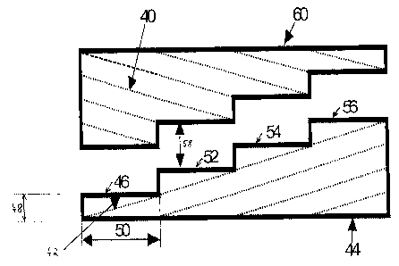
Figure 2 shows a first insulating wedge 40 located
opposite a second insulating wedge 42, and which could
in principle be used as the first insulating layer 26
or as the second insulating layer 32. However, this
figure shows only the basic design and the effect of
the arrangement of two insulating wedges 40, 42. To
this extent, the dimensions and the size relationships
in this figure are not to scale, and -are also not
comparable to the illustration in Figure 1.
The second insulating wedge 42 has a base side 44. A
first step 46, which has a first thickness 48 and a
step length .50, is intended to be arranged at a first
end of the base side 44. The first step 46 is adjacent
to a second step 52, which is offset by the first
thickness 48 with respect to the first step 46, so that
CA 02412349 2002-11-21
01/623 - 8 - 21 November 2001
the thickness of the second step 52 corresponds to the
two first. thicknesses 48 overall. This is followed in
the same way by a third step 54 and a fourth step 56,
which are added t:_o the first two steps 46, 52 to form a
staircase-like shape, with the third step 54 having a
thickness of three first layers 48, and the fourth step
56 having a thickness of four first steps 58. All the
step lengths of the steps 46, 52, 54, 56 correspond to
the step length 50. The upper faces of the steps, whose
lengths are referred to as step lengths 50, are each
arranged parallel to the base side 44.
The dimensions and structure of the first insulating
wedge 40 correspond exactly to those of the second
insulating wedge 42. However, in this view the section
through the first insulating wedge 40 is rotated
through 180 with respect to the second insulating
wedge 42. Furthermore, the first insulating wedge 40 is
positioned such that the respective step-shaped sides
of the insulating wedges 40, 42 are located exactly
opposite one another, and are arranged with a specific
gap 58, parallel to one another.
In the example shown in Figure 1, the first layer 18
could be arranged on the base side 44, with the second
layer 22 being arranged between the insulating wedges
40, 42, and the third layer 30 being arranged opposite
the base side of the first insulating wedge 40, which
corresponds to the base side 44. Figure 2 clearly shows
that the base side 44 and the side 60 are parallel to
one another and, accordingly, that the layers of
windings which are opposite these sides likewise come
to rest parallel to one another.