Note: Descriptions are shown in the official language in which they were submitted.
CA 02412370 2002-11-22
USE OF A U-GROOVE AS AN ALTERNATIVE TO USING A V-GROOVE
FOR PROTECTING SILICON AGAINST DICING INDUCED DAMAGE
BACKGROUND OF THE INVENTION AND
MATERIAL DISCLOSURE STATEMENT
The present invention relates generally to the fabrication of
semiconductor devices. In particular, to the dicing of integrated circuit
chips with great accuracy, and within close proximity to fabricated
elements on the chip. The invention relates, most particularly, to the dicing
of silicon sensor chips as employed for digital image sensors.
Image sensor dies for scanning document images, such as
Charge Coupled Devices (CCDs), typically have a row or linear array of
photo-sites together with suitable supporting circuitry integrated onto
silicon. Usually, a die of this type is used to scan line by line across the
width of a document with the document being moved or stepped
lengthwise in synchronism therewith.
In the above application, the image resolution is proportional to
the ratio of the scan width and the number of array photo-sites. Because
of the difficulty in economically designing and fabricating long dies, image
resolution for the typical die commercially available today is relatively low
when the die is used to scan a full line. While resolution may be improved
electronically as by interpolating extra image signals, or by interlacing
several smaller dies with one another in a non-collinear fashion so as to
crossover from one die to the next as scanning along the line progresses,
electronic manipulations of this type adds to both the complexity and the
cost of the system. Further, single or multiple die combinations such as
described above usually require more complex and expensive optical
systems.
However, a lon,g or full width array, having a length equal to or
larger than the document line and with a large packing of co-linear photo-
sites to assure high resolution, has been and remains a very desirable
arrangement. In the pursuit of a long or full width array, forming the array
by assembling several small dies together end to end has become an
CA 02412370 2006-03-02
exemplary arrangement. However, this necessitates providing dies whose photo-
sites extend to the border or edge of the die, so as to assure continuity when
the
die is assembled end to end with other dies, and at the same time provide
edges
that are sufficiently smooth and straight to be assembled together without
loss of
image data.
Although the standard technique of scribing and cleaving silicon wafers
used by the semiconductor industry for many years produces dies having
reasonably controlled dimensions, the microscopic damage occurring to the die
surface during the scribing operation has effectively precluded the
disposition of
the photo-sites at the die edge. This is because the top surface of silicon
wafers
is virtually always parallel to the <100> plane of the crystalline lattice so
that,
when a wafer of this type is cut or diced with a high speed diamond blade,
chips
and slivers are broken away from the top surface of the wafer in the direct
vicinity
of the channel created by the blade. This surface chipping typically extends
to
about 50 microns, thus, rendering it impossible for active elements to be
located
any closer than about 50 microns from the dicing channel. This as a result,
has
driven the adoption of V-shaped grooves as a technique for providing much
smoother dicing and thereby enabled tighter dicing accuracy and closer
proximity
of active chip elements to the chip/die edge.
U.S. Patent number 4,814,296 discloses a process for forming individual
dies having faces that allow the dies to be assembled against other like dies
to
form one and/or two dimensional scanning arrays wherein the active side of a
wafer is etched to form small V-shaped grooves defining the die faces,
relatively
wide grooves are cut in the inactive side of the wafer opposite each V-shaped
groove, and the wafer cut by sawing along the V-shaped grooves, the saw being
located so that the side of the saw blade facing the die is aligned with the
bottom
of the V-shaped groove so that there is retained intact one side of the V-
shaped
groove to intercept and prevent cracks and chipping caused by sawing from
damaging the die active surface and any circuits thereon.
However, utilization of a V-shaped groove technique while effective has
proven to be expensive. This expense may be broadly characterized as due
primarily to two things. Both of these arise from the
2
CA 02412370 2002-11-22
requirement for an anisotropic etch so as to maintain a V-groove wall
which is parallel to the <111> crystalline plane found in the wafer. First,
there are the extra foundry costs. An anisotropic etch is a wet etch and as
such is a non-standard process for most silicon foundries. This also means
that the wafers must be stripped of their photoresist and require extra
handling with placement in an off-line wet etch tool as well. Secondly,
there is the cost impact resulting from chip yield effects. Anisotropic
etching is by nature an aggressive etch due to the chemicals employed
and, thus, often attacks and damages the top layers of passivation oxide
and metal on the wafer. This is further exacerbated by the stripping of the
photoresist, which would otherwise act as a barrier layer and aid in
preventing wafer damage.
Therefore, as discussed above, there exists a need for an
arrangement and methodology which will solve the problem of preventing
cracks and chipping caused by damage from sawing while minimizing the
costs of doing so. Thus, it would be desirable to solve this and other
deficiencies and disadvantages as discussed above with an improved
semiconductor dicing methodology.
The present invention relates to a method for dicing die from a
semiconductor wafer while allowing a very close cut of a die edge relative
to active elements on the die without damaging the active elements. The
method steps comprise etching a U-groove via a dry etch in the
semiconductor wafer and sawing the semiconductor wafer along the U-
groove where one edge of the saw is substantially in alignment with the
bottom of the U-groove.
In particular, the present invention relates to a method for dicing
die from a semiconductor wafer while allowing a very close cut of a die
edge relative to active elements on the die without damaging the active
elements. The method steps comprising etching by way of a first dry etch
an opening down to the surface of the semiconductor wafer, followed by
etching by way of a second dry etch a U-groove in the opening down to the
surface of the semiconductor wafer created by the first dry etch, and then
sawing the semiconductor wafer along the U-groove where one edge of
the saw is substantially in alignment with the bottom of the U-groove.
-3-
CA 02412370 2007-11-08
The present invention also relates to a method of fabricating high
resolution image sensor dies from a wafer so that the dies have precision
faces
to enable the dies to be assembled with other like dies to form a larger array
without image loss or distortion at the points where the dies are assembled
together. The method comprising the steps of etching small U-shaped grooves in
one side of a wafer delineating the faces of the dies where the dies are to be
separated from the wafer. This is followed by forming grooves in the opposite
side of the wafer opposite each of the U-shaped grooves, the axis of the
grooves
being parallel to the axis of the U-shaped groove opposite thereto. In turn
this is
followed by, sawing the wafer along the U-shaped grooves with one side of the
cut made by sawing being substantially coextensive with the bottom of the U-
shaped grooves whereby one side of the U-shaped grooves is at least partially
obliterated by the sawing, the sides of the U-shaped grooves that remain
serving
to prevent development of fractures in the die beyond the remaining side as
the
wafer is being sawed.
In accordance with an aspect of the present invention, there is provided a
method for dicing die from a semiconductor wafer while allowing a very close
cut
of a die edge relative to active elements on the die without damaging the
active
elements comprising:
etching by way of a first dry etch an opening down to the surface of
the semiconductor wafer;
etching by way of a second dry etch a U-groove in the opening
down to the surface of the semiconductor wafer created by the first dry etch;
and
sawing the semiconductor wafer along the U-groove where one
edge of the saw is substantially in alignment with the bottom of the U-groove.
In accordance with another aspect of the present invention, there is
provided a method of fabricating high resolution image sensor dies from a
wafer
so that the dies have precision faces to enable the dies to be assembled with
other like dies to form a larger array without image loss or distortion at the
points
-4-
CA 02412370 2007-11-08
where the dies are assembled together, comprising the steps of:
etching by way of a first dry etch an opening down to the surface of
the semiconductor wafer;
etching by way of a second dry etch small U-shaped grooves in the
opening down to the surface of the semiconductor wafer created by the first
dry
etch;
forming grooves in the opposite side of the wafer opposite each of
the U-shaped grooves, the axis of the grooves being parallel to the axis of
the U-
shaped groove opposite thereto; and
sawing the wafer along the U-shaped grooves with one side of the
cut made by sawing being substantially coextensive with the bottom of the U-
shaped grooves whereby one side of the U-shaped grooves is at least partially
obliterated by the sawing, the sides of the U-shaped grooves that remain
serving
to prevent development of fractures in the die beyond the remaining side as
the
wafer is being sawed.
In accordance with a further aspect of the present invention, there is
provided a method for dicing die from a semiconductor wafer while allowing a
very close cut of a die edge relative to active elements on the die without
damaging the active elements comprising:
etching a U-groove via a dry etch in the semiconductor wafer
substrate; and
sawing the semiconductor wafer along the U-groove where one
edge of the saw is substantially in alignment with the bottom of the U-groove.
In accordance with another aspect of the present invention, there is
provided a method of fabricating high resolution image sensor dies from a
wafer
so that the dies have precision faces to enable the dies to be assembled with
other like dies to form a larger array without image loss or distortion at the
points
where the dies are assembled together, comprising the steps of:
etching small U-shaped grooves in one side of a wafer delineating
the faces of the dies where the dies are to be separated from the wafer;
-4a-
CA 02412370 2007-11-08
forming grooves in the opposite side of the wafer opposite each of
the U-shaped grooves, the axis of the grooves being parallel to the axis of
the U-
shaped groove opposite thereto; and
sawing the wafer along the U-shaped grooves with one side of the
cut made by sawing being substantially coextensive with the bottom of the U-
shaped grooves whereby one side of the U-shaped grooves is at least partially
obliterated by the sawing, the sides of the U-shaped grooves that remain
serving
to prevent development of fractures in the die beyond the remaining side as
the
wafer is being sawed.
BRIEF DESCRIPTION OF THE DRAWINGS
FIGURE 1 depicts a cross section of the wafer at the dicing channel and at
that process step where a groove is to be cut prior to the wet etch.
FIGURE 2 depicts the result after formation of a V-groove.
FIGURE 3 depicts the result after formation of a U-groove.
FIGURE 4 depicts the schematical representation of both a V-groove and
an U-groove for purposes of geometric comparison.
DESCRIPTION OF THE INVENTION
The prior approach employed of using a V-groove for dicing image sensor
dies as described above has associated with it increased costs, process cycle
time, reduced yield and increased metal layer defects. The disclosure taught
herein overcomes these disadvantages by replacing the V-groove with a U-
groove, using in one embodiment a dry etch consisting
-4b-
CA 02412370 2002-11-22
of SF6, He and 02. The intent of etching a V-groove into the silicon is to
relieve damage to the device caused by dicing the wafer. A U-groove has
proven itself as an improvement because the angle of the U-groove is
sufficient to deflect cracking and stress away from the device while only
requiring a dry etch for its achievement.
Figure 1 depicts a cross section of a wafer 100 comprising dies to
be diced. The cross section depicted is a SEM magnification of one dicing
channel on wafer 100. Here in Figure 1 is depicted the result after
photoresist 101 has been applied, exposed, and developed, and with a
io subsequent first dry etch performed to etch through any metal layers 102
as well as any TEOS 103 (Tetraethylorthosilicate) layers to reach the
silicon surface 104 of the silicon layer 105. This opens oxide opening 104
to about 6 microns in width in one preferred embodiment. The photoresist
101, at initially 22000 angstroms, is attacked by the first dry etch at a rate
of about 52 angstroms per second, leaving approximately 5000 angstroms
behind.
In Figure 2 there is depicted the result for a prior art V-groove
process. The photoresist of Figure 1 has been stripped away and the
wafer transferred to a wet etch tool for a Tetra methyl Ammonium
Hydroxide (TMAH) wet etch of 330 seconds. This TMAH etch has been
favored for its anisotropic etching effect, however it also attacks the final-
level metal through cracks in the TEOS passivation layers impacting chip
yield. In one typical embodiment, the V-groove 200 that results for an
approximate 6 micron opening will have an approximate depth of 4
microns and a total width with undercut of about 7.5 microns as typified in
the depiction provided in Figure 2.
The U-groove 300 is depicted in Figure 3. The U-groove process
begins the same as the V-groove process. However, it departs in its
process steps subsequent to the stage depicted in Figure 1. Unlike with
the V-groove process, whatever remains of the photoresist 101 is not
stripped. The photoresist 101 is left in place thereby eliminating the
stripping step and by virtue of retaining the photoresist 101 it also further
provides protection for the underlying metal and TEOS layers in the
following steps.
-5-
CA 02412370 2002-11-22
The next step in the methodology is to employ a second dry etch
consisting of SF6 and 02, and thereby create the U-groove 300 in silicon
layer 105 as shown in Figure 3. The original intent of etching a V-Groove
200 into the silicon 105 is to relieve damage to the die caused by dicing
the wafer. A U-Groove 300 is an acceptable alternative because the angle
of the groove is sufficient to deflect cracking and stress away from any
devices on the wafer 100. Replacing the V-Groove 200 with a U-Groove
300 results in cost savings, increased process throughput, improved yield
and reduced metal-3 defects, all by virtue of eliminating the wet TMAH
etch.
Table (1) shows parameter range median start points developed
for one U-Groove 300 embodiment. It will be well understood by those
skilled in the art that these parameters will vary from tool to tool, and that
it
is not useful to provide greater specifics. It will also be understood that
these parameters may be varied even upon the same tool, yet still achieve
the same results. Nevertheless, etching silicon is well understood in the
art, and those so skilled will be able with the table to practice the
invention
without undue experimentation. The reported etch time in the table of
about 75 seconds was needed for a 4 micron deep U-Groove 300, which is
also the approximate depth of the V-Groove 200 in one preferred
embodiment.
Table 1. U-Groove Etch Parameters for a.Dry Etch Tool
Parameter Median Start Points
Pressure Approximately 300 mTorr
RF Approximately 200 Watts
02 Flow Approximately 15 sccm
He Flow Approximately 65 sccm
SF6 Flow Approximately 175 sccm
Etch Time Approximately 75 seconds
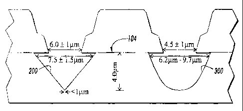
A schematic profile of a V-Groove and U-Groove is shown in
Figure 4 for comparison and to clarify the target dimensions. The desired
U-Groove 300 dimensions were derived from the specifications and
requirements set for V-Grooves and by the limitations in the U-Groove etch
process. The minimum V-Groove 200 depth is 3.5 microns and 7.5
-6-
CA 02412370 2006-03-02
microns wide, with an oxide opening of 6.0 microns and flat bottom less than 1
microns. U-Groove 300 specifications will be targeted to 4.5 1 microns for
both
the oxide opening and depth, with a U-Groove 300 width between 6.2 microns
and 9.7 microns. The desired variation in depth across the wafer is less than
15
percent. In achieving this, the U-Groove 300 oxide opening is best made
significantly smaller than the corresponding V-Groove oxide opening to help
reduce the overall U-Groove width. However, this is not a requirement to
practice
the invention. Substituting a new V-Groove mask is, therefore, used in one
embodiment to achieve an oxide opening of 4.5 microns for the U-Groove
process.
The subsequent steps for dicing the wafer into die are as is well known by
those skilled in the art, and also as described in U.S. Patent number
4,814,296.
A second groove is formed in the bottom or inactive surface of the wafer 100
opposite and parallel to each U-groove 300. The wafers are then typically
secured and cut using a suitable cutting device such as a high speed diamond
dicing blade.
In closing, by going to a U-groove profile and modifying the second etch to
be a dry etch instead of a wet etch results in a direct cost savings by
eliminating a
more expensive process step, as well as the need for stripping the developed
photoresist layer. Furthermore, going to a U-groove profile accomplishes
additional indirect and perhaps greater cost savings from the increased
process
throughput, improved yield, and reduced metal layer defects.
While the embodiments disclosed herein are preferred, it will be
appreciated from this teaching that various alternative, modifications,
variations
or improvements therein may be made by those skilled in the art. For example,
it
will be understood by those skilled in the art that the teachings provided
herein
may be applicable to other semiconductor types, including: gallium arsenide,
and
particularly to silicon on insulator, and amorphous silicon. There are also
many
other tool sets known to those skilled in the art with which to effectively
provide a
suitable dry etch as well as other combinations of etch rate, pressure, RF
energy,
gas rate, and etch time beyond those disclosed. All such variants of
processing
technique are intended to be encompassed by the following claims:
7