Language selection

Search

Patent 2412423 Summary

Third-party information liability

Some of the information on this Web page has been provided by external sources. The Government of Canada is not responsible for the accuracy, reliability or currency of the information supplied by external sources. Users wishing to rely upon this information should consult directly with the source of the information. Content provided by external sources is not subject to official languages, privacy and accessibility requirements.

Claims and Abstract availability

Any discrepancies in the text and image of the Claims and Abstract are due to differing posting times. Text of the Claims and Abstract are posted:

  • At the time the application is open to public inspection;
  • At the time of issue of the patent (grant).
(12) Patent: (11) CA 2412423
(54) English Title: IMPROVED TRANSPARENT SUBSTRATE LIGHT EMITTING DIODE
(54) French Title: DIODE EMETTRICE DE LUMIERE, A SUBSTRAT TRANSPARENT AMELIORE
Status: Expired
Bibliographic Data
(51) International Patent Classification (IPC):
  • H01L 33/10 (2010.01)
  • H01L 33/32 (2010.01)
(72) Inventors :
  • CHEN, JOHN (United States of America)
  • LIANG, BINGWEN (United States of America)
  • SHIH, ROBERT (United States of America)
(73) Owners :
  • DALIAN MEIMING EPITAXY TECHNOLOGY CO., LTD. (China)
(71) Applicants :
  • AMERICAN XTAL TECHNOLOGY, INC. (United States of America)
(74) Agent: GOWLING WLG (CANADA) LLP
(74) Associate agent:
(45) Issued: 2012-03-20
(86) PCT Filing Date: 2001-07-25
(87) Open to Public Inspection: 2002-01-31
Examination requested: 2006-07-18
Availability of licence: N/A
(25) Language of filing: English

Patent Cooperation Treaty (PCT): Yes
(86) PCT Filing Number: PCT/US2001/023347
(87) International Publication Number: WO2002/009243
(85) National Entry: 2002-12-20

(30) Application Priority Data:
Application No. Country/Territory Date
09/626,444 United States of America 2000-07-26

Abstracts

English Abstract


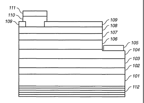
A gallium nitride based light emitting diode comprises both a transparent
substrate (101) and a window (109) for exiting light generated by the LED.
Useful amounts of light may be utilized at the face of the window (109) or at
the face of the transparent substrate (101). An external optical reflector
(112) is formed directly on the external face of the LED which is not
currently being used to exit useful light. If light from the window (109) is
being utilized, a Distributed Bragg Reflector, or DBR, (112) is formed
directly on the "backside" of the substrate. However, if light through the
substrate (101) is being utilized, a DBR (112) is formed directly on the light
emitting portion of the window (109).


French Abstract

Cette diode émettrice de lumière, à base de nitrure de gallium, comprend à la fois un substrat transparent (101) et une fenêtre (109) servant à la sortie de la lumière produite par la diode électroluminescente. Il est possible d'utiliser des quantités utiles de lumière au niveau de la face de la fenêtre (109) ou de la face du substrat transparent (101). Un réflecteur optique extérieur (112) est formé directement sur la face extérieure de la diode électroluminescente, lequel n'est généralement pas utilisé pour sortir la lumière utile. Si la lumière sortant de la fenêtre (109) est utilisée, un réflecteur Bragg réparti, ou DBR (112), est formé directement sur le côté arrière du substrat. Cependant si la lumière traversant le substrat (101) est utilisée, un réflecteur Bragg réparti (112) est formé directement sur la portion émettrice de lumière de la fenêtre (109).

Claims

Note: Claims are shown in the official language in which they were submitted.


-4-
What is claimed is:

1. A light emitting diode comprising a transparent substrate, a light emitting
region, and a
window wherein light generated by the light emitting diode exits through the
transparent
substrate;
characterized in that:
said light emitting diode further comprises:
a Distributed Bragg Reflector (DBR) that reflects light in a selected range of
wavelengths, the DBR being mounted directly on an external face of only the
window
which is not being used to exit light, such that the DBR is positioned
opposite to the side
from which the light exits the light emitting diode.

2. A light emitting diode in accordance with claim 1 wherein: said light
emitting
diode is constructed to generate light having a selected optical
characteristic; and said
DBR is formed to accommodate to said selected optical characteristic.

Description

Note: Descriptions are shown in the official language in which they were submitted.


CA 02412423 2002-12-20
WO 02/09243 PCT/USO1/23347
-1
TITLE
Improved Transparent Substrate Light Emitting Diode
TECHNICAL FIELD
This invention relates to Light Emitting Diodes having transparent
substrates.
BACKGROUND OF THE INVENTION
A semiconductor light-emitting diode (LED) comprises: a substrate; a light
emitting region; and a pair of electrodes for powering the diode. The
substrate
may be opaque or transparent. Light Emitting Diodes which are based on Gallium
Nitride compounds generally comprise: a transparent, insulating substrate,
e.g. a
sapphire substrate. With a transparent substrate, light may be utilized from
either
the substrate or from the opposite end of the LED which is termed the
"window".
The magnitude of the light emitted by an LED depends on: (a) The percent
of the light emitting region that is activated by current flowing between the
electrodes; (b) The efficiency of the window structure; and (c) The internal
losses
of generated light.
Where the light that exits through the window is being utilized, some of the
light directed to and through the transparent substrate is lost. Similarly,
were the
light that exits through the substrate is being utilized, some of the light
directed to
and through the window is lost.
DISCLOSURE OF THE INVENTION
In accordance with the present invention, an external optical reflector is
formed directly on the face of the LED which is not being used to exit useful
light.
If light from the window is being utilized, a reflector is formed directly on
the
"backside" of the substrate. However, if light through the substrate is being
utilized, a reflector is forined directly on the light emitting portion of the
window.
In accordance with this invention, a Distributed Bragg Reflector may be
formed on either the backside of the substrate or on the window.
Advantageously


CA 02412423 2002-12-20
WO 02/09243 PCT/USO1/23347
-2-
the light emitted is increased by 50 to 100 percent.
BRIEF DESCRIPTION OF THE DRAWING
Figs. 1 and 1 are schematic showings of the side views of two illustrative
embodiment of my improved LED.
DETAILED DESCRIPTION
The illustrative LEDs of Figs. 1 and 2 are GaN based devices. The devices
of Figs. 1 and 2 differ only in the placement of the reflectors 112 and 212.
In Fig.
l, the window 109 is utilized for the exit of light; and the reflector 112 is
formed
on the backside of substrate 101. In Fig. 2, the transparent substrate 101 is
utilized
for the exit of light; and the reflector 212 is formed on the window 109. The
elements of Fig. 2 which correspond to the elements of Fig. 1 bear the same
numerical labels.
The LED of Figs. 1 and 2 comprises: sapphire substrate 101; buffer region
102, GaN substitute substrate layer 103; N cladding layer 104, active region
106, P
cladding layer 107, window layers 108 and 109, N electrode 105, and P contact
assembly 110 and 111.
In Fig. l, light exits through window 109 and the DBR 112 is formed on
the backside of the substrate 101.
Layers 101 through 104, and layers 106 through 109 are grown in a Metal
Organic Chemical Vapor Deposition MOCVD reactor. The details of MOCVD
growth of the stated layers are well known in the industry and will not be
discussed herein.
The remaining components of the illustrative LED, namely, adhesion pad
110, P bond pad 11 l, and N bond pad 105 are formed by evaporation in
apparatus
other than a MOCVD reactor. Such processes are well lcnown in the prior art
and
are not described herein.
The details of the construction of the illustrative embodiments of the LED
of Fig. 1 are not important to the teachings of our invention. The present
invention is applicable to any light emitting diode that has a transparent
substrate


CA 02412423 2002-12-20
WO 02/09243 PCT/USO1/23347
-3=
i.e., sapphire substrate 101; and wherein light generated in the active region
i.e.,
region 106, reaches and passes through substrate 101.
The DBR reflectors, 112 and 212, are each designed to provide reflection
of light of a range of wavelengths arriving at range of incident angles. Each
DBR
comprises a number of pairs of layers to achieve the planned optical
characteristics.
The layers of a DBR, e.g., DBR 112, is fabricated in an evaporation
chamber by alternating the source materials which are deposited first on the
backside of substrate 101, and progressively on the grown layers. Growth of
the
layers of DBR 212 on layer 109 follows the same process.
The invention has been described with particular attention to its preferred
embodiment; however, it should be understood that variations and modifications
within the spirit and scope of the invention may occur to those slcilled in
the art to
which the invention pertains. For example, suitable layers of reflective
metals
may be substituted for the DBRs.

Representative Drawing
A single figure which represents the drawing illustrating the invention.
Administrative Status

For a clearer understanding of the status of the application/patent presented on this page, the site Disclaimer , as well as the definitions for Patent , Administrative Status , Maintenance Fee  and Payment History  should be consulted.

Administrative Status

Title Date
Forecasted Issue Date 2012-03-20
(86) PCT Filing Date 2001-07-25
(87) PCT Publication Date 2002-01-31
(85) National Entry 2002-12-20
Examination Requested 2006-07-18
(45) Issued 2012-03-20
Expired 2021-07-26

Abandonment History

There is no abandonment history.

Payment History

Fee Type Anniversary Year Due Date Amount Paid Paid Date
Application Fee $300.00 2002-12-20
Maintenance Fee - Application - New Act 2 2003-07-25 $100.00 2002-12-20
Registration of a document - section 124 $100.00 2003-12-11
Registration of a document - section 124 $100.00 2004-06-25
Maintenance Fee - Application - New Act 3 2004-07-26 $100.00 2004-07-02
Maintenance Fee - Application - New Act 4 2005-07-25 $100.00 2005-06-28
Request for Examination $800.00 2006-07-18
Maintenance Fee - Application - New Act 5 2006-07-25 $200.00 2006-07-19
Maintenance Fee - Application - New Act 6 2007-07-25 $200.00 2007-07-04
Maintenance Fee - Application - New Act 7 2008-07-25 $200.00 2008-07-07
Maintenance Fee - Application - New Act 8 2009-07-27 $200.00 2009-07-02
Maintenance Fee - Application - New Act 9 2010-07-26 $200.00 2010-07-08
Registration of a document - section 124 $100.00 2011-06-01
Maintenance Fee - Application - New Act 10 2011-07-25 $250.00 2011-07-12
Final Fee $300.00 2011-12-22
Maintenance Fee - Patent - New Act 11 2012-07-25 $250.00 2012-06-26
Maintenance Fee - Patent - New Act 12 2013-07-25 $250.00 2013-06-25
Maintenance Fee - Patent - New Act 13 2014-07-25 $250.00 2014-07-24
Maintenance Fee - Patent - New Act 14 2015-07-27 $250.00 2015-07-22
Maintenance Fee - Patent - New Act 15 2016-07-25 $450.00 2016-07-21
Maintenance Fee - Patent - New Act 16 2017-07-25 $450.00 2017-07-21
Maintenance Fee - Patent - New Act 17 2018-07-25 $450.00 2018-07-18
Maintenance Fee - Patent - New Act 18 2019-07-25 $450.00 2019-07-17
Maintenance Fee - Patent - New Act 19 2020-07-27 $450.00 2020-07-15
Owners on Record

Note: Records showing the ownership history in alphabetical order.

Current Owners on Record
DALIAN MEIMING EPITAXY TECHNOLOGY CO., LTD.
Past Owners on Record
AMERICAN XTAL TECHNOLOGY, INC.
AXT, INC.
CHEN, JOHN
LIANG, BINGWEN
LUMEI OPTOELECTRONICS CORP.
SHIH, ROBERT
Past Owners that do not appear in the "Owners on Record" listing will appear in other documentation within the application.
Documents

To view selected files, please enter reCAPTCHA code :


To view images, click a link in the Document Description column. To download the documents, select one or more checkboxes in the first column and then click the "Download Selected in PDF format (Zip Archive)" or the "Download Selected as Single PDF" button.

List of published and non-published patent-specific documents on the CPD .

If you have any difficulty accessing content, you can call the Client Service Centre at 1-866-997-1936 or send them an e-mail at CIPO Client Service Centre.


Document
Description 
Date
(yyyy-mm-dd) 
Number of pages   Size of Image (KB) 
Abstract 2002-12-20 2 64
Claims 2002-12-20 1 27
Drawings 2002-12-20 1 13
Description 2002-12-20 3 119
Representative Drawing 2002-12-20 1 6
Cover Page 2004-01-22 1 39
Claims 2010-08-27 1 20
Cover Page 2012-02-20 1 39
Representative Drawing 2012-02-23 1 6
Prosecution-Amendment 2010-08-27 4 143
PCT 2002-12-20 1 40
Assignment 2004-06-25 15 557
PCT 2002-12-20 2 84
Assignment 2002-12-20 3 124
Correspondence 2003-02-27 1 25
Correspondence 2003-02-27 1 16
Correspondence 2003-07-04 1 29
Assignment 2003-12-11 7 233
Correspondence 2004-01-19 1 26
Correspondence 2004-02-18 1 36
Correspondence 2004-05-25 2 121
Maintenance Fee Payment 2017-07-21 2 52
Prosecution-Amendment 2006-07-18 1 42
Prosecution-Amendment 2007-01-29 1 26
Correspondence 2008-08-12 2 64
Correspondence 2008-08-20 1 14
Correspondence 2008-08-20 1 17
Prosecution-Amendment 2010-03-02 3 80
Fees 2010-07-08 1 40
Assignment 2011-06-01 5 161
Correspondence 2011-12-22 2 50