Note: Descriptions are shown in the official language in which they were submitted.
CA 02413329 2002-12-27
WO 02/03407 PCT/USO1/19887
IMPLANTABLE MEDICAL DEVICE HAVING
FLAT ELECTROLYTIC CAPACITOR WITH
MINIATURIZED EPOXY CONNECTOR DROPLET
FIELD OF THE INVENTION
This invention relates to implantable medical devices (IMDs) and their various
components, including flat electrolytic capacitors for same, and methods of
making and
using same, particularly a simplified, miniature capacitor connector block and
wiring
to harness utilizing an epoxy droplet and method of making same.
BACKGROUND OF THE INVENTION
As described in the above-referenced parent application Serial No. 09/104,104,
and
the provisional application that it claims priority from, a wide variety of
IMDs are known
is in the art. Ofparticular interest are implantable cardioverter-
defibrillators (ICDs) that
deliver relatively high energy cardioversion and/or defibrillation shocks to a
patient's heart
when a malignant tachyarrhythmia, e.g., atrial or ventricular fibrillation, is
detected.
Current ICDs typically possess single or dual chamber pacing capabilities for
treating
specified chronic or episodic atrial and/or ventricular bradycardia and
tachycardia and
~ o were referred to previously as pacemaker/cardioverter/defibrillators
(PCDs). Earlier
developed automatic implantable defibrillators (AIDs) did not have
cardioversion or
pacing capabilities. For purposes of the present invention ICDs are understood
to
encompass all such IMDs having at least high voltage cardioversion and/or
defibrillation
capabilities.
z5 Generally speaking, it is necessary to employ a DC-DC converter within an
ICD
implantable pulse generator (IPG) to convert electrical energy from a low
voltage, low
current, electrochemical cell or battery enclosed within the IPG housing to a
high voltage
energy level stored in one or more high energy storage capacitor, as shown for
example, in
commonly assigned U.S. Patent No. 4,548,209. The conversion is effected upon
3 o confirmation of a tachyarrhythmia by a DC-DC "flyback" converter which
includes a
transformer having a primary winding in series with the battery and a
secondary winding
in series with the high energy capacitors) and an interrupting circuit or
switch in series
with the primary coil and battery that is periodically opened and closed
during a charging
CA 02413329 2002-12-27
WO 02/03407 PCT/USO1/19887
2
cycle. Charging of the high energy capacitor is accomplished by inducing a
voltage in the
primary winding of the transformer creating a magnetic field in the secondary
winding
when the switch is closed. The field collapses when the current in the primary
winding is
interrupted by opening the switch, and the collapsing field develops a current
in the
s secondary winding which is applied to the high energy capacitor to charge
it. The repeated
interruption of the supply current charges the high energy capacitor to a
desired level of
several hundred volts over a charging time of the charge cycle. Then, the
energy is rapidly
discharged from the high voltage capacitors) through
cardioversion/defibrillation
electrodes coupled to the IPG through ICD leads and arranged about or in a
heart chamber
or vessel if the tachyarrhythmia is confirmed as continuing at the end of the
charge time.
The cardioversion/defibrillation shocks effected by discharge of such
capacitors are
typically in the range of about 25 to 40 Joules. The process of delivering
cardioversionldefibrillation shocks in this way may be repeated if an earlier
delivered
cardioversion/defibrillation shock does not convert the tachyarrhythmia to a
normal heart
rhythm.
Energy, volume, thickness and mass are critical features in the design of ICD
pulse
generators that are coupled to the ICD leads. The battery(s) and high voltage
capacitors)
used to provide and accumulate the energy required for the
cardioversion/defibrillation
shocks have historically been relatively bulky and expensive. Presently, ICD
IPGs
a o typically have a volume of about 40 to about 60 cc, a thickness of about
13 mm to about
16 mm and a mass of approximately 100 grams.
It is desirable to reduce the volume, thickness and mass of such capacitors
and ICD
IPGs without reducing deliverable energy. Doing so is beneficial to patient
comfort and
minimizes complications due to erosion of tissue around the ICD IPG.
Reductions in size
as of the capacitors may also allow for the balanced addition of volume to the
battery,
thereby increasing longevity of the ICD IPG, or balanced addition of new
components,
thereby adding functionality to the ICD IPG. It is also desirable to provide
such ICD IPGs
at low cost while retaining the highest level of performance. At the same
time, reliability
of the capacitors cannot be compromised.
CA 02413329 2002-12-27
WO 02/03407 PCT/USO1/19887
Various types of flat and spiral-wound capacitors are known in the art, some
examples of which are described as follows and/or may be found in the patents
listed in
Table 1 of the above-referenced parent patent application Serial No.
09/104,104.
Prior art high voltage electrolytic capacitors used in ICDs have two or more
anode
and cathode layers (or "electrodes") and operate at room or body temperature.
Typically,
the capacitor is formed with a capacitor case enclosing an etched aluminum
foil anode, an
aluminum foil or film cathode, and a Kraft paper or fabric gauze spacer or
separator
impregnated with a solvent based liquid electrolyte interposed therebetween. A
layer of
aluminum oxide that functions as a dielectric layer is formed on the etched
aluminum
1 o anode, preferably during passage of electrical current through the anode.
The electrolyte
comprises an ion producing salt that is dissolved in a solvent and provides
ionic electrical
conductivity between the cathode and the aluminum oxide dielectric. The energy
of the
capacitor is stored in the electrostatic field generated by opposing
electrical charges
separated by the aluminum oxide layer disposed on the surface of the anode and
is
15 proportional to the surface area of the aluminum anode. Thus, to minimize
the overall
volume of the capacitor one must maximize anode surface area per unit volume
without
increasing the capacitor's overall (i.e., external) dimensions. The separator
material,
anode and cathode layer terminals, internal packaging, electrical
interconnections, and
alignment features and cathode material further increase the thickness and
volume of a
a o capacitor. Consequently, these and other components in a capacitor and the
desired
capacitance limit the extent to which its physical dimensions may be reduced.
Some ICD IPGs employ commercial photoflash capacitors similar to those
described by Troup in "Implantable Cardioverters and Defibrillators," Current
Problems in
CardioloQV, Volume XIV, Number 12, Dec. 1989, Year Book Medical Publishers,
25 Chicago, and as described in U.S. Patent No. 4,254,775. The electrodes or
anode and
cathodes are wound into anode and cathode layers separated by separator layers
of the
spiral. Anode layers employed in such photoflash capacitors typically comprise
one or
two sheets of a high purity (99.99%), porous, highly etched, anodized aluminum
foil.
Cathode layers in such capacitors are formed of a non-porous, highly etched
aluminum foil
s o sheet which may be somewhat less pure (99.7%) respecting aluminum content
than the
anode layers. The separator formed of one or more sheet or layer of Kraft
paper saturated
CA 02413329 2002-12-27
WO 02/03407 PCT/USO1/19887
4
and impregnated with a solvent based liquid electrolyte is located between
adjacent anode
and cathode layers. The anode foil thickness and cathode foil thickness are on
the order of
100 micrometers and 20 micrometers, respectively. Most commercial photoflash
capacitors contain a core of separator paper intended to prevent brittle,
highly etched
s aluminum anode foils from fracturing during winding of the anode, cathode
and separator
layers into a coiled configuration. The cylindrical shape and paper core of
commercial
photoflash capacitors limits the volumetric packaging efficiency and thickness
of an ICD
IPG housing made using same.
The aluminum anodes and cathodes of aluminum electrolytic capacitors generally
1 o each have at least one tab extending beyond their perimeters to facilitate
electrical
connection of all (or sets of) the anode and cathode layers electrically in
parallel to form
one or more capacitor and to make electrical connections to the exterior of
the capacitor
case. Tab terminal connections for a wound electrolytic capacitor are
described in U.S.
Patent No 4,663,824 that are laser welded to feedthrough pin terminals of
feedthroughs
is extending through the case. Wound capacitors usually contain two or more
tabs joined
together by crimping or riveting.
Flat electrolytic capacitors have also been disclosed in the prior art for
general
applications as well as for use in ICDs. More recently developed ICD IPGs
employ one or
more flat high voltage capacitor to overcome some of the packaging and volume
2 o disadvantages associated with cylindrical photoflash capacitors. For
example, U.S. Patent
No. 5,131,388 discloses a flat capacitor having a plurality of stacked
capacitor layers.
each comprising an "electrode stack sub-assembly". Each capacitor layer
contains one or
more anode sheet forming an anode layer having an anode tab, a cathode sheet
or layer
having a cathode tab and a separator for separating the anode layer from the
cathode layer.
25 In the '388 patent, the electrode stack assembly of stacked capacitor
layers is encased
within a non-conductive, polymer envelope that is sealed at its seams and
fitted into a
chamber of a conductive metal, capacitor case or into a compartment of the ICD
IPG
housing, and electrical connections with the capacitor anodes) and cathodes)
are made
through feedthroughs extending through the case or compartment wall. The tabs
of the
3 o anode layers and the cathode layers of all of the capacitor layers of the
stack are
electrically connected in parallel to form a single capacitor or grouped to
form a plurality
CA 02413329 2002-12-27
WO 02/03407 PCT/USO1/19887
of capacitors. The aluminum anode layer tabs are gathered together and
electrically
connected to a feedthrough pin of an anode feedthrough extending through the
case or
compartment wall. The aluminum cathode layer tabs are gathered together and
electrically
connected to a feedthrough pin of a cathode feedthrough extending through the
case or
s compartment wall or connected to the electrically conductive capacitor case
wall.
Many improvements in the design of flat aluminum electrolytic capacitors for
use
in ICD IPGs have been disclosed, e.g., those improvements described in "High
Energy
Density, Capacitors for Implantable Defibrillators" presented by P. Lunsmann
and D.
MacFarlane at CARTS 96: 16th Capacitor and Resistor Technolo~y Symposium, 11-
15
to March 1996, and at CARTS-EUROPE 96: 10th European Passive Components
Symposium., 7-11 October 1996, pp. 35-39. Further features of flat
electrolytic capacitors
for use in ICD IPGs are disclosed in U.S. Patent Nos. 4,942,501; 5,086,374;
5,146,391;
5,153,820; 5,562,801; 5,584,890; 5,628,801; and 5,748,439, all issued to
MacFarlane et
al.
A number of recent patents including U.S. Patent No. 5,660,737 and U.S. Patent
Nos.5,522,851; 5,801,917; 5,808,857; 5,814,082; 5,908,151; 5,922,215;
5,926,357;
5,930,109; 5,968,210 and 5,983,472, all assigned to the same assignee,
disclose related
flat electrolytic capacitor designs for use in ICDs. In several of these
patents, internal
alignment elements are employed as a means for controlling the relative edge
spacing of
a o the anode and cathode layers from the conductive capacitor case. In these
patents, each
anode layer and cathode layer is provided with an outwardly extending tab, and
the anode
and cathode tabs are electrically connected in common to a feedthrough pin and
a step
feature of the conductive capacitor case, respectively. The cathode tabs are
gathered
together against the step feature and ultrasonically welded together and to
the step feature.
In the '357 patent, the anode tabs are laser welded to one end of an aluminum
ribbon that
is ultrasonically welded at its other end to an aluminum layer that is
ultrasonically welded
to the terminal pin. The feedthrough terminal pin is electrically isolated
from and extends
outside and away from the case to provide an anode connection pin. A cathode
connection
pin is attached to the case and extends outwardly therefrom. The anode and
cathode
s o connection pins are electrically connected into the DC-DC converter
circuitry, but the
attachment mechanism is not described in any detail.
CA 02413329 2002-12-27
WO 02/03407 PCT/USO1/19887
6
Other ways of sealing the capacitor cases and making electrical connections
with
the anodes and cathodes through or to the capacitor case are disclosed in the
prior art. One
construction employed from about 1960 to about 1985 and disclosed in U.S.
Patent No.
4,521,830 uses a plastic header with two molded-in threaded aluminum terminals
of the
type shown in U.S. Patent No. 3,789,502, where plastic is molded around the
terminals.
An aluminum serrated shank terminal extending through a thermal plastic header
is
disclosed in U.S. Patent Nos. 3,398,333 and 4,183,600. In both patents the
aluminum
terminal is resistance-heated to a temperature such that the length of the
terminal is
collapsed and the center diameter is increased to press the serrations into
the melted
to plastic. A header design employing a compression-fit set of terminals
disposed in a
polymer header is also disclosed.
A glass-to-metal seal terminal connection L1~e- A
a PO Yf (-
Z < Z < <~<~<~
C~<~$-~ ~ ~ ~ ~-
-' ~ d ~- de L ' ' (' (' ('
(' (' (' "b $b $b $b!& 3b -Ec ~ Fe
°e-T f U-de <~('
a o (' (~ (~ de (~ <~<~
<~(, ..b yz'i\
<~<~(~ ..b (,
In one embodiment, the capacitor comprises an electrode stack assembly and
electrolyte are located within the interior case chamber of a hermetically
sealed capacitor
case. The electrode stack comprises a plurality of capacitor layers stacked in
registration
upon one another, each capacitor layer comprising a cathode layer having a
cathode tab, an
s o anode sub-assembly comprising at least one anode layer having an anode
tab, and a
separator layer located between adjacent anode and cathode layers, whereby all
adjacent
CA 02413329 2002-12-27
WO 02/03407 PCT/USO1/19887
7
cathode layers and anode layers of the stack are electrically insulated from
one another by
a separator layer. Anode terminal means extend through the capacitor case side
wall for
electrically connecting a plurality of the anode tabs to one another and
providing an anode
connection terminal at the exterior of the case. Cathode terminal means extend
through or
s to an encapsulation area of the capacitor case side wall for electrically
connecting a
plurality of the cathode tabs to one another and providing a cathode
connection terminal at
the exterior of the case. A connector assembly is electrically attached to the
anode
connection terminal for making electrical connection with the anode tabs and
to the
cathode connection terminal for making electrical connection with the cathode
tabs.
s o In accordance with the invention, a connector block is formed of an epoxy
droplet
adhered to the encapsulation area of the capacitor side wall surrounding and
encapsulating
the anode and cathode connection terminals and the electrical connections with
the
connector assembly.
The connector block is formed on an encapsulation area of the case side wall
of
is epoxy that is cured for a period of time under elevated temperature
conditions while
rotating the capacitor assembly. The epoxy is applied in a liquid state, and
the rotation and
temperature causes the epoxy to flow into gaps of and to completely cover the
anode and
cathode terminal means and the electrical connections with the connector
assembly, to
drive air bubbles to the exposed surface, and to shape the exterior surface to
1a uniform,
a o repeatable configuration.
At least one edge of the encapsulation area is preferably masked to restrict
flow of
epoxy out of the encapsulation area when it is applied and during curing.
In case neutral capacitors, the anode and cathode terminal means comprise a
feedthrough assembly fitted into an opening in the encapsulation area of the
capacitor case
as side wall. The anode and cathode feedthrough assemblies further comprise
anode and
cathode feedthrough pins coupled at an internal pin end with the plurality of
anode and
cathode tabs, respectively. Electrically insulating spacers support and
electrically insulate
the feedthrough pins from the capacitor case and disposing the external pin
ends away
from the case to provide the anode and cathode connection terminals. A portion
of the
s o epoxy droplet flows into the spacers around the terminal pins toward the
interior case
chamber to seal the feedthrough assemblies to prevent leakage of electrolyte.
Preferably,
CA 02413329 2002-12-27
WO 02/03407 PCT/USO1/19887
exposed wire ends of the connector assembly are electrically and mechanically
coupled to
the external pin ends, preferably by cross-wire welding.
In one case negative capacitor embodiment, the cathode terminal means
comprises
means for electrically connecting the plurality of cathode tabs to the case
side wall to
s provide the cathode connection terminal upon the case side wall within the
encapsulation
area. An exposed wire end of the connector assembly is attached to the case
wall within
the encapsulation area.
In a further case negative embodiment, the cathode terminal means comprises a
cathode feedthrough pin extending through the case side wall having an
internal pin end
to connected to the plurality of cathode tabs and an external pin end
extending away from the
case to provide the cathode connection terminal, the cathode feedthrough pin
electrically
'connected with the case. Preferably, an exposed wire end of the connector
assembly is
electrically and mechanically coupled to the cathode external pin end,
preferably by cross-
wire welding.
15 The epoxy droplet provides a reliable, reproducible, inexpensive,
attractive,
miniaturized connection of the connector assembly with the anode and cathode
tabs.
BRIEF DESCRIPTION OF THE DRAWINGS
These and other advantages and features of the present invention will be
appreciated as
z o the same becomes better understood by reference to the following detailed
description of the
preferred embodiment of the invention when considered in connection with the
accompanying drawings, in which like numbered reference numbers designate like
parts
throughout the figures thereof, and wherein:
FIG. 1 illustrates the physical components of one exemplary embodiment of an
25 ICD IPG and lead system in which the present invention may be
advantageously
incorporated;
FIG. 2 is a simplified functional block diagram illustrating the
interconnection of
voltage conversion circuitry with the high voltage capacitors of the present
invention with
the primary functional components of one type of an ICD;
CA 02413329 2002-12-27
WO 02/03407 PCT/USO1/19887
9
FIGs. 3(a) -3(g) are exploded perspective views of the manner in which the
various
components of the exemplary ICD IPG of FIGS. 1 and 2, including the
electrolytic
capacitors of the present invention, are disposed within the housing of the
ICD IPG;
FIG. 4 is an exploded view of one embodiment of a single anode/cathode layer
or
s electrode stack sub-assembly of an electrolytic capacitor incorporating the
present
invention;
FIG. 5(a) is an exploded perspective view of one embodiment of a cold welding
apparatus in which anode layers of the electrode stack sub-assembly of FIG. 4
are cold-
welded;
so FIG. 5(b) is an unexploded view of the cold welding apparatus of FIG. 5(a);
FIG. 5(c) is a cross-sectional view of the cold welding apparatus of FIGS.
5(a) and
5(b) in which anode layers of the electrode sub-assembly of FIG. 4 are cold-
welded
therein;
FIG. 6(a) is an exploded top perspective view of one embodiment of a stack of
is anode/cathode layer sub-assemblies into a stacked electrode stack assembly
of an
electrolytic capacitor incorporating the present invention;
FIG. 6(b) is a cross-sectional view of a portion of one embodiment of a cold-
welded anode assembly used in the electrolytic capacitor;
FIG. 6(c) is a cross-sectional view of another portion of one embodiment of a
cold-
a o welded anode assembly used in the electrolytic capacitor;
FIG. 7 is a top perspective view of one embodiment of an electrode stack
assembly
of an electrolytic capacitor incorporating the present invention;
FIG. 8 is an enlarged view of a portion of the electrode stack assembly shown
in
FIG. 7;
25 FIG. 9 is an exploded top perspective view of one embodiment of a case
neutral
capacitor of the present invention employing the electrode stack assembly of
FIGS. 6, 7
and 8 therein;
FIG. 10 is an exploded top perspective view of the partially assembled
capacitor of
FIG. 9;
3 o FIG. 11 is a top view of one embodiment of a partly assembled capacitor of
the
present invention having no cover disposed thereon;
CA 02413329 2002-12-27
WO 02/03407 PCT/USO1/19887
FIG. 12 is a top perspective view of the capacitor of FIG. 11 having a cover
disposed thereon.
FIG. 13 is a flow chart of one method of the present invention for making a
case
neutral or case negative capacitor incorporating the present invention;
FIG. 14 is a flow chart of one method for making an anode layer of a capacitor
incorporating the present invention;
FIG. 15 is a flow chart of one method for making an electrode stack assembly
of a
capacitor incorporating the present invention;
FIG. 16 is a flow chart of one method for making tab interconnections and
to feedthrough terminal connections of a capacitor incorporating the present
invention;
FIG. 17 is a flow chart of one method for making tab interconnections and
feedthrough terminal connections of a capacitor incorporating the present
invention;
FIG. 1 ~ is a flow chart of one method for making a case sub-assembly of a
capacitor incorporating the present invention;
is FIG. 19 is a flow chart of one method for sealing a case and cover of a
capacitor
incorporating the present invention;
FIG. 20 is a flow chart of one method for sealing a feedthrough of a capacitor
incorporating the present invention;
FIGS. 21 (a) -21 (c) are top views of the case neutral capacitor assembly
during the
a o fabrication of the epoxy droplet connector block about the connection of
the wiring
harness and the anode and cathode feedthrough pins;
FIGs. 22(a) and 22(b) are side elevation views of two embodiments of
miniaturized, case negative or case floating, capacitors formed with epoxy
droplet
connector blocks;
2s FIG. 23(a) is a side elevation view in partial exposed section illustrating
one
embodiment of the electrical connections of the gathered anode and cathode
tabs with the
wiring harness within the epoxy droplet connector block;
FIG. 23(b) is an end perspective view illustrating the electrical connections
of the
feedthrough terminal pins of FIG. 23(a) with the wiring harness within the
epoxy droplet
s o connector block;
CA 02413329 2002-12-27
WO 02/03407 PCT/USO1/19887
11
FIG. 24(a) is a side elevation view in partial exposed section illustrating a
further
embodiment of the electrical connections of the gathered anode and cathode
tabs with the
wiring harness within the epoxy droplet connector block; and
FIG. 24(b) is an end perspective view illustrating the electrical connections
of the
wiring harness with the anode feedthrough terminal pin and the case of FIG.
24(a) within
the epoxy droplet connector block.
DETAILED DESCRIPTION OF THE PREFERRED EMBODIMENTS
FIG. 1 illustrates one embodiment of ICD IPG 10 in which the capacitor of the
to present invention is advantageously incorporated, the associated ICD
electrical leads 14,
16 and 18, and their relationship to a human heart 12. The leads are coupled
to ICD IPG
by means of mufti-port connector block 20, which contains separate connector
ports for
each of the three leads illustrated. Lead 14 is coupled to subcutaneous
electrode 30, which
is intended to be mounted subcutaneously in the region of the left chest. Lead
I 6 is a
coronary sinus lead employing an elongated coil electrode which is located in
the coronary
sinus and great vein region of the heart. The location of the electrode is
illustrated in
broken line format at 32, and extends around the heart from a point within the
opening of
the coronary sinus to a point in the vicinity of the Left atrial appendage.
Lead 18 is provided with elongated electrode coil 28 which is located in the
right
a o ventricle of the heart. Lead 18 also includes stimulation electrode 34
which takes the form
of a helical coil which is screwed into the myocardial tissue of the right
ventricle. Lead 18
may also include one or more additional electrodes for near and far field
electrogram
sensing.
In the system illustrated, cardiac pacing pulses axe delivered between helical
2s electrode 34 and elongated electrode 28. Electrodes 28 and 34 are also
employed to sense
electrical signals indicative of ventricular contractions. As illustrated, it
is anticipated that
the right ventricular electrode 28 will serve as the common electrode during
sequential and
simultaneous pulse multiple electrode defibrillation regimens. For example,
during a
simultaneous pulse defibrillation regimen, pulses would simultaneously be
delivered
s o between electrode 28 and electrode 30 and between electrode 28 and
electrode 32. During
sequential pulse defibrillation, it is envisioned that pulses would be
delivered sequentially
CA 02413329 2002-12-27
WO 02/03407 PCT/USO1/19887
12
between subcutaneous electrode 30 and electrode 28 and between coronary sinus
electrode
32 and right ventricular electrode 28. Single pulse, two electrode
defibrillation shock
regimens may be also provided, typically between electrode 28 and coronary
sinus
electrode 32. Alternatively, single pulses may be delivered between electrodes
28 and 30.
s The particular interconnection of the electrodes to an ICD will depend
somewhat on which
specific single electrode pair defibrillation shock regimen is believed more
likely to be
employed.
FIG. 2 is a block diagram illustrating the interconnection of high voltage
output
circuit 40, high voltage charging circuit 64 and capacitors 265 according to
one example of
~. o the microcomputer based operating system of the ICD IPG of FIG. 1. As
illustrated, the
ICD operations are controlled by means of a stored program in microprocessor
42, which
performs all necessary computational functions within the ICD. Microprocessor
42 is
linked to control circuitry 44 by means of bi-directional data/control bus 46,
and thereby
controls operation of the output circuitry 40 and the high voltage charging
circuitry 64.
15 Pace/sense circuitry 78 awakens microprocessor 42 to perform any necessary
mathematical calculations, to perform tachycardia and fibrillation detection
procedures and
to update the time intervals controlled by the timers in pace/sense circuitry
78 on
reprogramming of the ICD operating modes or parameter values or on the
occurrence of
signals indicative of delivery of cardiac pacing pulses or of the occurrence
of cardiac
~ o contractions,.
The basic operation and particular structure or components of the exemplary
ICD
of FIGS. 1 and 2 may correspond to any of the systems known in the art, and
the present
invention is not dependent upon any particular configuration thereof. The flat
aluminum
electrolytic capacitor of the present invention may be employed generally in
conjunction
as with the various systems illustrated in the aforementioned '209 patent, or
in conjunction
with the various systems or components disclosed in the various U.S. patents
listed in the
above-referenced parent patent application Serial No. 09/104,104.
Control circuitry 44 provides three signals of primary importance to output
circuitry 40. Those signals include the first and second control signals
discussed above,
s o labeled here as ENAB, line 48, and ENBA, line 50. Also of importance is
DUMP line 52
which initiates discharge of the output capacitors and VCAP line 54 which
provides a
CA 02413329 2002-12-27
WO 02/03407 PCT/USO1/19887
13
signal indicative of the voltage stored on the output capacitors C1, C2, to
control circuitry
44. Defibrillation electrodes 28, 30 and 32 illustrated in FIG. 1, above, are
shown coupled
to output circuitry 40 by means of conductors 22, 24 and 26. For ease of
understanding,
those conductors are also labeled as "COMMON", "HVA" and "HVB". However, other
s configurations are also possible. For example, subcutaneous electrode 30 may
be coupled
to HVB conductor 26, to allow for a single pulse regimen to be delivered
between
electrodes 28 and 30. During a logic signal on ENAB, line 48, a
cardioversion/defibrillation shock is delivered between electrode 30 and
electrode 28.
During a logic signal on ENBA, line 50, a cardioversion/ defibrillation shock
is delivered
to between electrode 32 and electrode 28.
The output circuitry includes a capacitor bank, including capacitors C 1 and
C2 and
diodes 121 and 123, used for delivering defibrillation shocks to the
electrodes.
Alternatively, the capacitor bank may include a further set of capacitors as
depicted in the
above referenced '758 application. In FIG. 2, capacitors 265 are illustrated
in conjunction
is with high voltage charging circuitry 64, controlled by the control/timing
circuitry 44 by
means of CHDR line 66. As illustrated, capacitors 265 are charged by means of
a high
frequency, high voltage transformer 65. Proper charging polarities are
maintained by
means of the diodes 121 and 123. VCAP line 54 provides a signal indicative of
the
voltage on the capacitor bank, and allows for control of the high voltage
charging circuitry
z o and for termination of the charging function when the measured voltage
equals the
programmed charging level.
Pace/sense circuitry 78 includes an R-wave sense amplifier and a pulse
generator
for generating cardiac pacing pulses, which may also correspond to any known
cardiac
pacemaker output circuitry and includes timing circuitry for defining
ventricular pacing
z s intervals, refractory intervals and blanking intervals, under control of
microprocessor 42
via control/data bus 80.
Control signals triggering generation of cardiac pacing pulses by pace/sense
circuitry 78 and signals indicative of the occurrence of R-waves, from
pace/sense circuitry
78 are communicated to control circuitry 44 by means of a bi-directional data
bus 81.
3 o Pace/sense circuitry 78 is coupled to helical electrode 34 illustrated in
FIG. 1 by means of
a conductor 36. Pace/sense circuitry 78 is also coupled to ventricular
electrode 28,
CA 02413329 2002-12-27
WO 02/03407 PCT/USO1/19887
14
illustrated in FIG. 1, by means of a conductor 82, allowing for bipolar
sensing of R-waves
between electrodes 34 and 28 and for delivery of bipolar pacing pulses between
electrodes
34 and 28, as discussed above.
FIGs. 3(a) through 3(g) show perspective views of various components of ICD
IPG
10, including one embodiment of the capacitor of the present invention, as
those
components are placed successively within the housing of ICD IPG 10 formed by
right
and left hand shields 240 and 350.
In FIG. 3(a), electronics module 360 is placed in right-hand shield 340 of ICD
IPG
10. FIG. 3(b) shows ICD IPG 10 once electronics module 360 has been seated in
right-
1 o hand shield 340.
FIG. 3(c) shows a pair of capacitors 265 formed as described herein prior to
being
placed within right-hand shield 340, the capacitors 265 being connected
electrically in
series by interconnections in electronics module 340. FIG. 3(d) shows ICD IPG
10 once
the pair of capacitors 265 has been placed within right-hand shield 340. In
accordance
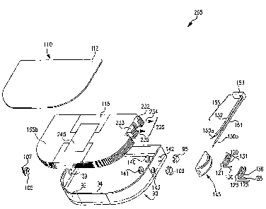
15 with one aspect of the present invention, the space occupied by the epoxy
droplet
connector block 145 and wire harness 155 of each stacked capacitor 265 within
right-hand
shield 340 is advantageously minimized. It will be understood that other
shapes of
capacitors 265 utilizing the improved connector block 145 and wiring harness
155 of the
present invention can be inserted into the housing of ICD IPG 10 in the same
or similar
a o manner as described here.
FIG. 3(e) shows insulator cup 370 prior to its placing atop capacitors 265 in
right-
hand shield 340. FIG. 3(f) shows electrochemical cell or battery 380 having
insulator 382
disposed around battery 380 prior to placing it in shield 340. Battery 380
provides the
electrical energy required to charge and re-charge capacitors 265, and also
powers
2s electronics module 360. Battery 380 rnay take any of the forms employed in
the prior art
to provide cardioversion/defibrillation energy, some of which are identified
in parent
patent application Serial No. 09/104,104.
FIG. 3(g) shows ICD IPG 10 having left-hand shield 350 connected to right-hand
shield 340 and feedthrough 390 projecting upwardly from both shield halves.
Activity
3 o sensor 400 and patient alert apparatus 410 are shown disposed on the side
lower portion of
CA 02413329 2002-12-27
WO 02/03407 PCT/USO1/19887
left-hand shield 350. Left-hand shield 350 and right-hand shield 340 are
subsequently
closed and hermetically sealed (not shown in the figures).
FIG. 4 shows an exploded view of one embodiment of a capacitor layer or single
anode/cathode sub-assembly 227 of capacitor 265. The capacitor design
described herein
s employs a stacked configuration of a plurality of capacitor layers or single
anode/cathode
sub-assemblies 227 as further described below with respect to FIG. 6. Each
anode/cathode
sub-assembly 227 comprises alternating substantially rectangular-shaped anode
layers 185
and cathode layers 175, with a substantially rectangular-shaped separator
layer 180 being
interposed therebetween. The shapes of anode layers 185, cathode layers 175
and
to separator layers 180 are primarily a matter of design choice, and are
dictated largely by the
shape or configuration of case 90 within which those layers are ultimately
disposed.
Anode layers 185, cathode layers 175 and separator layers 180 may assume any
arbitrary
shape to optimize packaging efficiency.
Anode sub-assembly 170d most preferably comprises a plurality of non-notched
is anode layers 185a, 185b, 185c, notched anode layer 190 including anode tab
notch 200,
and anode tab 195 coupled to anode layer 185a. It will be understood that
anode sub-
assembly 170d shown in FIG. 4 is but one possible embodiment of an anode sub-
assembly
170. Cathode layer 175d most preferably is formed of a single sheet and has
cathode tab
176 formed integral thereto and projecting from the periphery thereof.
a o In one preferred embodiment of the sub-assembly 227 as depicted in the
figures,
two individual separator layer sheets 180a and 180b form the separator layer
180 that is
disposed between each anode sub-assembly 170 and cathode layer 175. Further
single
separator layer sheets 180a and 180b are disposed against the outer surfaces
of the anode
layer 185c and the cathode layer 175d. When the sub-assemblies are stacked,
the
outermost single separator layer sheets 180a and 180b bear against adjacent
outermost
single separator layer sheets 180b and 180a, respectively, of adjacent
capacitor layers so
that two sheet separator layers 180 separate all adjacent cathode and anode
layers of an
electrode stack assembly 225.
It will be understood by those skilled in the art that the precise number of
sub-
3 o assemblies 227 selected for use in a electrode stack assembly 225 will
depend upon the
energy density, volume, voltage, current, energy output and other requirements
placed
CA 02413329 2002-12-27
WO 02/03407 PCT/USO1/19887
16
upon capacitor 265. Similarly, it will be understood by those skilled in the
art that the
precise number of notched and un-notched anode layers 185, anode tabs 195,
anode sub-
assemblies 170, cathode layers 175 and separator layers 180 selected for use
in a given
embodiment of anode/cathode sub-assembly 227 will depend upon the energy
density,
s volume, voltage, current, energy output and other requirements placed upon
capacitor 265.
It will now become apparent that a virtually unlimited number of combinations
and
permutations respecting the number of anode/cathode sub-assemblies 227, and
the number
of un-notched and notched anode layers 185 forming anode sub-assembly 170,
anode sub-
assemblies 170, anode tabs 195, cathode layers 175 and separator layers 180
disposed
1 o within each anode/cathode sub-assembly 227, may be selected according to
the particular
requirements of capacitor 265. Anode layers 185, cathode layers 175 and
separator layers
180 are most preferably formed of materials typically used in high quality
aluminum
electrolytic capacitors.
Anode layers 185 and 190 are formed of anode foil that is most preferably
through-
is etched, has a high specific capacitance (at least about 0.3, at least about
0.5 or most
preferably at least about 0.8 microfarads/cm2), has a dielectric withstand
parameter of at
least 425 Volts DC, a thickness ranging between about 50 and about 200
micrometers,
more preferably between about 75 and 150 micrometers, more preferably yet
between
about 90 and about 125 micrometers, and most preferably being about 100
micrometers
2o thick, and a cleanliness of about 1.0 mg/mz respecting projected area
maximum chloride
contamination. The anode foil preferably has a rated surge voltage of 390
Volts, an initial
purity of about 99.99% aluminum, a final thickness of about 104 micrometers,
plus or
minus about five micrometers, and a specific capacitance of about 0.8
microfarads per
square centimeter. Suitable anode foils are commercially available on a
widespread basis.
25 Individual anode layers 185 are typically somewhat stiff and formed of high-
purity
aluminum processed by etching to achieve high capacitance per unit area. Thin
anode
foils are preferred, especially if they substantially maintain or increase
specific capacitance
while reducing the thickness of the electrode stack assembly 225, or maintain
the thiclaiess
of electrode stack assembly 225 while increasing overall capacitance. For
example, it is
3 o contemplated that individual anode layers 185 have a thickness of about 10
micrometers,
about 20 micrometers, about 30 micrometers, about 40 micrometers, about 50
CA 02413329 2002-12-27
WO 02/03407 PCT/USO1/19887
17
micrometers, about 60 micrometers, about 70 micrometers, about 80 micrometers,
about
90 micrometers, about 100 micrometers, about 110 micrometers, about 120
micrometers,
about 130 micrometers, about 140 micrometers and about 150 micrometers.
Cathode layers 175 are preferably high purity and are comparatively flexible.
Cathode layers 175 are most preferably formed from cathode foil having high
surface area
(i.e., highly etched cathode foil), high specific capacitance (preferably at
least 200
microfarads/cm2, and at least 250 microfarads/cmz when fresh), a thickness of
about 30
micrometers, a cleanliness of about 1.0 mg/mZ respecting projected area
maximum
chloride contamination, and a purity which may be less than corresponding to
the starting
1 o foil material from which anode foil is made. The cathode foil preferably
has an initial
purity of at least 99% aluminum, and more preferably yet of about 99.4%
aluminum, a
final thickness of about 30 micrometers, and an initial specific capacitance
of about 250
microfarads per square centimeter. In other embodiments, cathode foil has a
specific
capacitance ranging between about 100 and about 500 microfarads/cm2, about 200
and
is about 400 microfarads/cmz, or about 250 and about 350 microfarads/cmz, a
thickness
ranging between about 10 and about 150 micrometers, about 15 and about 100
micrometers, about 20 and about 50 micrometers, or about 25 and about 40
micrometers.
It is generally preferred that the specific capacitance of the cathode foil be
as high
as possible, and that cathode layer 175 be as thin as possible. For example,
it is
a o contemplated that individual cathode layers 175 have specific capacitances
of about 100
microfarads/cm2, about 200 microfarads/cm2, about 300 microfarads/cm2, about
400
microfarads/cm2, about 500 microfarads/cmz, about 600 microfarads/cm2, about
700
microfarads/cm2, about 800 microfarads/cmz, about 900 microfarads/cm2, or
about 1,000
microfarads/cmz. Suitable cathode foils are commercially available on a
widespread basis.
25 In still other embodiments, cathode foil is formed of materials or metals
in addition to
aluminum, aluminum alloys and "pure" aluminum.
Separator layer sheets 180a and 180b outer separator layers 165a and 165b are
most preferably made from a roll or sheet of separator material. Separator
layers 180 are
preferably cut slightly larger than anode sub-assemblies 170 and cathode
layers 175 to
3 o accommodate misalignment during the stacking of layers, to prevent
subsequent shorting
CA 02413329 2002-12-27
WO 02/03407 PCT/USO1/19887
18
between anode and cathode layers, and to otherwise ensure that a physical
barrier is
disposed between the anodes and the cathodes of the finished capacitor.
It is preferred that separator layer sheets 180a and 180b and exterior
separator
layers 165a and 165b (shown in FIG. 9) be formed of a material that: (a) is
chemically
inert; (b) is chemically compatible with the selected electrolyte; (c) may be
impregnated
with the electrolyte to produce a low resistance path between adjoining anode
and cathode
layers, and (d) physically separates adjoining anode and cathode layers. In
one preferred
embodiment, separator material is a pure cellulose, very low halide or
chloride content
Kraft paper having a thickness of about 0.0005 inches (0.0013 mm), a density
of about
l0 1.06 grams/cm3, a dielectric strength of 1,400 Volts AC per 0.001 inch
(0.025 rnm)
thickness, and a low number of conducting paths (about 0.4/ftz or less).
Separator layer
sheets 180a and 180b and outer separator layers 165a and 165b may also be
formed of
materials other than Kraft paper, such as Manila paper, porous polymeric
materials or
fabric gauze materials. For example, porous polymeric materials may be
disposed
is between anode and cathode layers like those disclosed in U.S. Patent
Numbers 3,555,369
and 3,883,784 in some embodiments of the capacitor layers
In such capacitor stacks formed of a plurality of capacitor layers, a liquid
electrolyte saturates or wets separator layers 180 and is disposed within case
90. It is to be
understood, however, that various embodiments include within their scope a
solid or .
a o adhesive electrolyte such as those disclosed in U.S. Patent Numbers,
5,628,801;
5,584,890; 4,942,501; 5,146,391 and 5,153,820. Note that an appropriate inter-
electrode
adhesives/electrolyte layer may be employed in place of paper, gauze or porous
polymeric
materials to form separator layer 180.
Continuing to refer to FIG. 4, a first preferred step in assembling a flat
aluminum
25 electrolytic capacitor is to cut anode layers 185 and 190, anode tabs 195,
cathode layers
175 and separator layers 180. Those components are most preferably cut to
shape using
dies having low wall-to-wall clearance, where inter-wall spacing between the
substantially
vertically-oriented corresponding walls of the punch and die is most
preferably on the
order of about 6 millionths of an inch per side. Larger or smaller inter-wall
spacings
s o between the substantially vertically-oriented corresponding walls of the
punch and cavity,
CA 02413329 2002-12-27
WO 02/03407 PCT/USO1/19887
19
such as about 2, about 4, about 5, about 7, about 8, about 10 and about 12
millionths of an
inch may also be employed but are less preferred.
Such low clearance results in smooth, burr free edges being formed along the
peripheries of anode layers 185 and 190, anode tabs 195, cathode layers 175
and separator
layers 180. Smooth, burr free edges on the walls of the dies have been
discovered to be
critical respecting reliable performance of a capacitor. The presence of burrs
along the
peripheries of anode layers 185 and 190, anode tabs 195, cathode layers 175
and separator
layers 180 may result in short circuit and failure of the capacitor. The means
by which
anode foil, cathode foil and separator materials are cut or formed may have a
significant
1 o impact on the lack or presence of burrs and other cutting debris disposed
about the
peripheries of the formed or cut members. The use of low clearance dies
produces an edge
superior to the edge produced by other cutting methods, such as steel rule
dies. The shape,
flexibility and speed of a low clearance die have been discovered to be
superior to those
achieved by laser or blade cutting. Other methods of cutting or forming anode
layers 185
is and 190, anode tabs 195, cathode layers 175 and separator layers 180
include, but are not
limited to, steel rule die cutting, laser cutting, water jet cutting and blade
cutting.
The preferred low clearance of the die apparatus is especially important for
cutting
thin ductile materials such as the cathode foil. In addition to improving
reliability, burr
and debris reduction permits reductions in the thickness of separator layer
180, thereby
2 o improving energy density of the capacitor. Angle cutting, where the face
of the punch is
not held parallel to the opposing floor of the die during the cutting step, is
another less
preferred method of cutting or forming anode layers 185 and 190, anode tabs
195, cathode
layers 175 and separator layers 180.
It is preferred to cut or otherwise form separator layer 180 such that its
outer
25 periphery conforms closely to that of the corresponding side walls of the
interior of case
90. In preferred embodiments, the periphery of separator layer is disposed
within plus or
minus 0.009 inches of the corresponding side walls of case 90. Such close
conformity
between the periphery of separator layer 180 and the corresponding internal
side walls of
case 90 has been discovered to provide the advantage of permitting separator
layers 180 to
3 o immobilize or secure firmly in place electrode stack assembly 225 in case
90. This
immobilization occurs because the separator paper forming separator layers 180
swells
CA 02413329 2002-12-27
WO 02/03407 PCT/USO1/19887
after electrolyte is added through the lumen of fill port 107 into otherwise
assembled and
sealed capacitor 265.
In a preferred method, foil or separator materials are drawn between the punch
and
cavity portions of a die having appropriate clearances on a roll. An air or
hydraulically
s actuated press is then most preferably employed to actuate the punch or
cavity portion of
the die. The punch portion of the die is most preferably formed of hardened
tool steel, or
has other suitable wear resistant materials or coatings disposed on the
cutting surfaces
thereof. When the cavity of the die is aligned vertically, the punch portion
of the die may
travel either upwards or downwards towards the die cavity during a cutting
cycle. In the
to former case, components are cut and drop downwardly into a container for
use in
subsequent assembly operations. In the latter case, components are cut and may
be
presented directly to automated assembly equipment, such as robots equipped
with
vacuum or other pick-up tooling, for subsequent processing. Low clearance dies
of the
type described herein may be supplied by Top Tool, Inc. of Minneapolis,
Minnesota.
15 Anode sub-assembly 170 most preferably includes one notched anode layer
190,
which facilitates appropriate placing and positioning of anode tab 195 within
anode sub-
assembly 170. More than one notched anode layer 190 may also be included in
anode sub-
assembly 170. It is preferred that the remaining anode layers of anode sub-
assembly 170
be non-notched anode layers 185. Anode tab 195 is most preferably formed of
aluminum
z o strip material. In one preferred embodiment, aluminum strip 80 has a
purity of about
99.99% aluminum and a lesser degree of anodization than anode foil 65. When
anode tab
195 is formed of a non-anodized material, cold welding of anode tab 195 to non-
notched
anode layers 185 may be accomplished with less force and deflection, more
about which
we say below. It is preferred that the thickness of anode tab 195 be about
equal to that of
as notched anode layer 190. If more than one notched anode layer 190 is
employed in anode
sub-assembly 170, a thicker anode tab 195 may be employed.
FIG. 13 shows a flow chart that describes generally one method, from beginning
to
end, of making flat aluminum electrolytic capacitor 265. FIGS. 14 through 20,
on the
other hand, show specific portions of the method or process described
generally in FIG.
13. .
CA 02413329 2002-12-27
WO 02/03407 PCT/USO1/19887
21
FIG. 14 shows a flow chart of one method for making anode layer 170 wherein
non-notched anode layers 185, notched anode layer 190 and anode tab 195 are
provided
and assembled within cold welder 202 to form anode sub-assembly 170.
Referring now to FIGS. 5(a) through 5(c), two non-notched anode layers 185a
and
185b are placed on cold welding fixture base layer 207 of cold welding
apparatus 202.
The various structural members of cold welding apparatus 202 are most
preferably formed
of precision machined stainless steel or a high strength aluminum alloy.
Layers 185a and
185b are next aligned and positioned appropriately on cold welding fixture
base layer 207
using spring loaded alignment pins 209a through 209e. Pins 209a through 209e
retract
s o upon top layer 208 being pressed downwardly upon layers 185a and 185b
disposed within
cold welding cavity 220. See also FIG. 5(c), where a cross-sectional view of
cold welding
apparatus 202 is shown.
Anode layer 190 is similarly disposed within cavity 220, followed by placing
anode tab 195 within anode tab notch 200 in notched anode layer 190. Anode tab
195 is
is most preferably positioned along the periphery of notched anode layer 190
with the aid of
additional spring loaded alignment pins 209f and 209g disposed along the
periphery of
anode tab 195. Non-notched anode layer 185c is then placed atop anode layer
190.
Stacked anode sub-assembly 170 is then clamped between top plate 208 and base
plate
207. Disposed within base plate 207 are anode layer cold welding pins 206a and
anode tab
a o cold welding pin 211 a. Disposed within top plate 208 are anode layer cold
welding pin
206b and anode tab cold welding pin 211b. Base plate 207 and top plate 208 are
aligned
such that the axes of cold welding pins 206a and 206b coincide with and are
aligned
respecting corresponding cold welding pins 211a and 211b.
Upper actuation apparatus 214 of cold welding apparatus 202 displaces cold
25 welding pins 206b and 21 1b downwardly. Lower actuation apparatus 215
displaces cold
welding pins 206a and 211a upwardly. In one embodiment of upper actuation
apparatus
214 and lower actuation apparatus 215, pneumatic cylinders are employed to
move pins
206a, 206b, 211a and 211b. In another embodiment of apparatus 214 and
apparatus 215, a
pair of rolling wheels is provided that move simultaneously and
perpendicularly to the
3 o axes of pins 206a, 206b, 211 a, and 21 1b. Still other embodiments of
apparatus 214 and
apparatus 215 may employ hydraulic actuators, cantilever beams, dead weights,
springs,
CA 02413329 2002-12-27
WO 02/03407 PCT/USO1/19887
22
servomotors electromechanical solenoids, and the like for moving pins 206a,
206b, 211 a
and 21 1b. Control of actuation apparatus 214 and apparatus 215 respecting pin
displacement force magnitude and timing may be accomplished using any one or
combination of constant load, constant displacement, solenoid controller,
direct or indirect
means.
Following clamping with top plate 208, cold welding pins 206a, 206b, 211a and
211b are actuated. Cold welds 205 and 210 in anode sub-assembly 170 are formed
by
compression forces generated when cold weld pins 206a, 206b, 211 a and 21 1b
are
compressed against anode sub-assembly 170. See FIG. 6(a), where the preferred
regions
s o in which cold welds 205 and 210 are formed are shown. Cold welds 205 and
210 may be
described as not only cold welds, but forged welds. This is because the
interfacial
boundaries between anode layers 185 are deformed in the region of welds 205
and 210,
thereby disrupting oxide layers and bringing base metals into direct contact
with one
another where metallic bonding occurs. Metallic bonding increases the strength
of the
is welds.
In one embodiment of the method, a plurality of pneumatic cylinders function
simultaneously in upper actuation apparatus 214 and lower actuation apparatus
215 to
drive pins 206a, 206b, 211a and 211b against anode sub-assembly 170. Anode
layer cold
weld 205 and anode tab cold weld 210 are most preferably formed under direct
constant
2 0 load conditions, where pneumatic cylinders are pressurized to a
predetermined fixed
pressure. Anode layer cold weld 205 and anode tab cold weld 210 may also be
formed
under indirect constant displacement conditions, where pneumatic cylinders are
pressurized until a displacement sensor placed across cold welding pins 206a,
206b, 211 a
or 21 1b generates a signal having a predetermined value, whereupon those pins
are
25 disengaged from anode/cathode sub-assembly 227.
In another embodiment of the method, a cantilever beam mechanism is
incorporated into upper actuation apparatus 214 and lower actuation apparatus
215.
Anode layer cold weld 205 and anode tab cold weld 210 are formed under direct
constant
displacement conditions, where cantilever beams are actuated and cause upper
and lower
3 o members 208 and 207 to engage anode/cathode sub-assembly 227 until a hard
stop point is
reached. An indirect load controlled system may also be employed in apparatus
214 and
CA 02413329 2002-12-27
WO 02/03407 PCT/USO1/19887
23
apparatus 215, where cantilever or other means include a load measuring sensor
for
controlling the stop point of the cantilever beam, for example, when a
predetermined load
is measured by the sensor.
The cross-sectional shape of cold weld pins 206a, 206b, 211 a and 211b may be
s square, circular, oval or any other suitable shape. The shape of the ends of
cold weld pins
206a, 206b, 211a and 21 1b may be flat, rounded, domed or any other suitable
shape
appropriate for selectively controlling the properties of the cold welds
produced therein.
Likewise, more or fewer than four cold weld pins may be employed. The ends of
cold
weld pins 206a, 206b, 211a and 21 1b are most preferably rounded or domed and
circular
1 o in cross-section. Cold weld pins 206a, 206b, 211 a and 21 1b preferably
have a diameter of
about 0.060 inches (0.174 mm) and further have a beveled or radiused end. Cold
weld
pins 206a, 206b, 211 a and 211b are preferably made from a high strength
material that
does not readily deform under the pressures obtained during welding, such as
stainless
steel, titanium, tool steel or HSLA steel. The ends or side walls of cold
welding pins 206a,
25 206b, 211a and 211b may be coated, clad or otherwise modified to increase
wear
resistance, deformation resistance or other desirable tribilogical attributes
of the pins.
The primary function of cold welds 205 and 210 is to provide electrical
interconnections between layers 185a, 185b, 185c and 190 and anode tab 195,
while
minimizing the overall thickness of anode sub-assembly 170 in the regions of
welds 205
2 0 . and 210. Typical prior art commercial cylindrical capacitors exhibit a
significant increase
in the thickness of the anode layer in the regions of the cold welds. This
increase in
thickness is typically on the order of about two times the thickness of the
tab, or about
0.008 inch (0.020 mm). In the case of cylindrical capacitors where only one or
two non-
coincident tab connections are present, the overall effect on anode layer
thickness may be
a s minimal. In a stacked layer design having many more interconnections and
welds,
however, increases in weld zone thickness have been found to significantly
increase the
overall thickness of the anode layer and the electrode stack assembly as a
whole.
In one cold welding method and corresponding apparatus, no or an inappreciable
net increase in anode sub-assembly 170 thickness results when cold weld
geometries and
s o formation processes are appropriately optimized. Several embodiments of
anode
assembly 170 have been found to have no more than about a 20% increase in
layer
CA 02413329 2002-12-27
WO 02/03407 PCT/USO1/19887
24
thickness due to the presence of cold welds, as compared to about a 200%
increase in
thickness resulting from cold welds found in some commercial cylindrical
capacitors.
Two, three, four, five, six or more anode layers 185 and 190 may be cold-
welded to form
anode sub-assembly 170 as described herein.
FIG. 6(b) shows a cross-sectional view of a portion of one embodiment of a
cold-
welded anode assembly formed in accordance with the preferred cold welding
method.
Anode layers 185a, 190, 185b and 185c having anode layer thicknesses to ,tN
,tb and t~ ,
respectively, are cold-welded together at weld 205 through the compressive
action of pins
206a and 206b mounted in bottom plate 207 and top plate 208, respectively.
Pins 206a
1 o and 206b form central depressions 293 and 294, respectively, in anode sub-
assembly 170d,
and further result in the formation of rims 295 and 296, respectively. Rims
295 and 296
project downwardly and upwardly, respectively, from the surrounding surfaces
of anode
sub-assembly 170d, thereby increasing the overall thickness T of anode sub-
assembly
170d by 0T (T measured in respect of the non-cold-welded surrounding regions
or
15 portions of anode sub-assembly 170d).
FIG. 6(c) shows a cross-sectional view of another portion of one embodiment of
a
cold-welded anode assembly wherein anode layers 185a, 185b and 185c and anode
tab
195, having anode layerltab thicknesses to ,tb, t~ and tab, respectively, are
cold-welded
together at weld 210 through the compressive action of pins 21 la and 21 1b
mounted in
2o bottom plate 207 and top plate 208, respectively. Pins 211a and 211b form
central
depressions 297 and 298, respectively, in anode sub-assembly 170d, and further
result in
the formation of rims 299 and 301, respectively. Rims 299 and 301 project
downwardly
and upwardly, respectively, from the surface of anode sub-assembly 170d,
thereby
increasing overall thickness T of anode sub-assembly 170d by ~T (T measured in
respect
as of the non-cold-welded surrounding regions or portions of anode sub-
assembly 170d).
The overall thickness T of anode sub-assembly 170d is therefore defined by the
equation: -
T= nt
CA 02413329 2002-12-27
WO 02/03407 PCT/USO1/19887
The maximum overall thickness T + ~T of anode sub-assembly 170d in the region
of cold
welds 205 or 210 is then defined by the equation:
T+ ~T=nt+OT
where T~S is the overall thickness of anode sub-assembly 170d in non-cold-
welded regions,
n is the number of anode layers 185 and/or 190 in anode sub-assembly 170d, and
t is the
thickness of individual anode layers 185 and/or 190 or anode tab 195 where the
thiclcnesses t", to ,tb, t~ and trab, are assumed to be the same.
to It is highly desirable to form anode sub-assembly such that the ratio OT/T
is less
than or equal to 0.05, 0.1, 0.15, 0.20, 0.25, 0.30, 0.35, 0.40, 0.45 or 0.50.
The lower the
value of the ratio OT/T, the greater the volumetric efficiency of capacitor
265.
Additionally, the overall thickness of capacitor 265 may be reduced when the
value of the
ratio OT/T is made smaller.
15 Referring now to FIG. 6(a), the overall thickness of electrode stack
assembly 225
may be reduced further by staggering or offsetting horizontally the respective
vertical
locations of tabs 195a through 195h (and corresponding cold welds 210). In
this
embodiment, tabs 195a 195b, for example, are not aligned vertically in respect
of one
another. Such staggering or offsetting of tabs 195 permits the increases in
thickness ~T
a o corresponding to each of anode subassemblies 170a through 170h to be
spread out
horizontally over the perimeter or other portion of electrode stack assembly
225 such that
increases in thickness DT do not accumulate or add constructively, thereby
decreasing the
overall thickness of electrode stack assembly 225. Cold welds 205 may
similarly be
staggered or offset horizontally respecting one another and cold weld 210 to
achieve a
z5 reduction in overall thickness of electrode stack assembly 225.
In another preferred embodiment, the anode sub-assembly 170 of each capacitor
layer or electrode sub-assembly comprises a plurality of three, four, five or
more anode
sheets or layers 185 and 190, each sub-assembly most preferably having at
least one anode
layer having a corresponding anode tab 195 attached thereto or forming a
portion thereof,
s o the layers being cold welded together to form anode sub-assembly 170. For
example, an
anode sub-assembly 170 may comprise six anode layers 185 constructed by cold-
welding
CA 02413329 2002-12-27
WO 02/03407 PCT/USO1/19887
26
two separate triple anode layers 185 that were previously and separately cold-
welded or
otherwise joined together. Alternatively, anode sub-assembly 170 layer may
comprise
seven anode layers constructed by cold-welding together one triple anode layer
185 and
one quadruple anode layer 185 that were previously and separately cold-welded
or
otherwise joined together. In another preferred embodiment, multiple notched
anode
layers 190 may employed in anode sub-assembly 170, thereby permitting the use
of a
thicker anode tab material.
The geometry of base plate 207 and top plate 208 in the regions surrounding
cold
welding pins 206a, 206b, 211a and 21 1b has been discovered to affect the
properties of
to cold welds 205 and 210. In a preferred method, the mating surfaces of
plates 207.and 208
surfaces have no radiused break formed in the perimeters of the pin holes. The
presence of
radiused breaks or chamfers in those regions may cause undesired deformation
of cold
welds 205 and 210 therein. Such defornzation may result in an increase in the
thickness of
anode sub-assembly 170, which may translate directly into an increase in the
thickness of
capacitor 265. Note further that the increase in thickness so resulting is a
multiple of the
number of anode sub-assemblies 170 present in electrode stack assembly 225.
Alternatively, radiused breaks or chamfers may be employed in the region of
the pin holes
in base plate 207 and top plate 208, but appropriate capacitor design
accommodations are
most preferably made, such as staggering the positions of adjoining stacked
cold welds.
a o As shown in FIG. 14, once cold welding pins 206a, 206b, 211a and 211b have
been actuated against anode sub-assembly 170, top plate 208 is removed and
cold-welded
anode sub-assembly 170 is provided for further stacking of anode/cathode sub-
assembly
227. FIG. 15 shows a flow chart corresponding to one preferred method for
making
electrode stack assembly 225. See also FIG. 6(a), where an exploded top
perspective view
as of one embodiment of an electrode stack assembly 225 of capacitor 265 is
shown. As
illustrated in FIGS. 4, 6(a) and 15, electrode stack assembly 225 most
preferably comprises
a plurality of cold-welded anode sub-assemblies 175a through 175h, a plurality
of cathode
layers 175a through 175i, a plurality of separator layers 180, outer separator
layers 165a
and 165b, outer wrap 115 and wrapping tape 245.
3 o Outer wrap 115 is most preferably die cut from separator material
described supra,
but may be formed from a wide range of other suitable materials such as
polymeric
CA 02413329 2002-12-27
WO 02/03407 PCT/USO1/19887
27
materials, aluminum, suitable heat shrink materials, suitable rubberized
materials and
synthetic equivalents or derivatives thereof, and the like.
Wrapping tape 245 is most preferably cut from a polypropylene-backed acrylic
adhesive tape, but may also be replaced by a staple, an ultrasonic paper joint
or weld,
suitable adhesives other than acrylic adhesive, suitable tape other than
polypropylene-
backed tape, a hook and corresponding clasp and so on.
Outer wrap 115 and wrapping tape 245 together comprise an electrode stack
assembly wrap which has been discovered to help prevent undesired movement or
shifting
of electrode stack assembly 225 during subsequent processing. It will now
become
so apparent to one skilled in the art that many means other than those
disclosed explicitly
herein exist for immobilizing and securing electrode stack assembly 225 during
subsequent processing which accomplish substantially the same function as the
electrode
stack assembly wrap comprising outer wrap 115 and wrapping tape 245.
Alternative
means for immobilizing and securing electrode stack assembly 225 other than
those
15 described hereinabove exist. Such alternative means include, but are not
limited to,
robotic or other mechanical clamping and securing means not necessarily
forming a
portion of electrode stack assembly 225, adhesive electrolytes for forming
separator layers
180, and so on.
The stacking process by which electrode stack assembly 225 is most preferably
z o made begins by placing outer wrap 115 into a stacking fixture followed by
placing outer
paper or separator layer 165a thereon. Next, cathode layer 175a is placed atop
separator
layer 165a, followed by separator layers 180a and 180b being disposed thereon.
Cold-
welded anode sub-assembly 170a is then placed atop separator layer 180b,
followed by
placing separator layers 180a and 180b thereon, and so on. The placing of
alternating
25 cathode layers 175 and anode sub-assemblies 170 with separator layers 180a
and 180b
interposed therebetween continues in the stacking fixture until final cathode
layer 175h has
been placed thereon.
In the embodiment of electrode stack assembly 225 shown in FIG. 6(a), eight
anode sub-assemblies (anode sub-assemblies 170a through 170h) and nine cathode
layers
30 (cathode layers 175a through 175i) are illustrated. The voltage developed
across each
combined anode sub-assembly/separator layer/cathode layer assembly disposed
within
CA 02413329 2002-12-27
WO 02/03407 PCT/USO1/19887
28
electrode stack assembly 225 most preferably ranges between about 360 and
about 390
Volts DC. As described below, the various anode sub-assemblies of electrode
stack
assembly 225 are typically connected in parallel electrically, as are the
various cathode
layers of electrode stack assembly 225.
Consistent with the discussion hereinabove concerning FIG. 4, it will now be
understood by one skilled in the art that electrode stack assembly 225 shown
in FIG. 6(a)
is merely illustrative, and does not limit the scope of the present invention
in any way
respecting the number or combination of anode sub-assemblies 170, cathode
layers 175,
separator layers 180, anode tabs 195, cathode tabs 176, and so on. The number
of
so electrode components is instead determined according to the total
capacitance required, the
total area of each layer, the specific capacitance of the foil employed and
other factors.
In another embodiment of electrode stack assembly 225, the number of anode
layers 185 employed in each anode sub-assembly 170 is varied in the stack.
Such a design
permits the fabrication of capacitors having the same layer area but nearly
continuously
is varying different and selectable total capacitances that a user may
determine by increasing
or decreasing the number of anode layers 185/190 included in selected anode
sub-
assemblies 170 (as opposed to adding or subtracting full anode/cathode sub-
assemblies
227 from electrode stack assembly 225 to thereby change the total
capacitance).
Following placing of cathode layer 1751 in the stack, outer paper layer 165b
is placed
z o thereon, and outer wrap 115 is folded over the top of electrode stack
assembly 225.
Wrapping tape 245 then holds outer wrap 115 in place and secures the various
components
of electrode stack assembly 225 together.
The physical dimensions of separator layers 165 and 180 are most preferably
somewhat larger than those of anode sub-assemblies 170 and cathode layers 175
to prevent
z5 contact of the electrodes with the case wall or electrical shorting between
opposing
polarity electrode layers due to the presence of burrs, stray or particulate
material, debris
or imperfections occurring therein. The reliability and functionality of
capacitor 265 may
be compromised if a portion of anode sub-assembly 170 comes into contact with
a
conducting case wall, if a burr on the periphery of anode sub-assembly 170 or
cathode
30 layer 175 comes into contact with an adjoining layer of opposing polarity,
or if separator
layer 180a or 180b does not provide sufficient electrical insulation between
adjoining
CA 02413329 2002-12-27
WO 02/03407 PCT/USO1/19887
29
opposite-polarity electrode layers and conducting particulate matter bridges
the gap
therebetween.
The additional separator material most preferably disposed about the periphery
of
electrode stack assembly 225 is referred to herein as separator overhang.
Decreasing the
s amount of separator overhang increases the energy density of capacitor 265.
It is
beneficial from an energy density optimization perspective, therefore, to
decrease the
amount or degree of separator overhang. _ The amount of separator overhang
required has
been discovered to be primarily a fiznction of the stack-up tolerance
characteristic of the
stacking method employed.
to In commercial cylindrical capacitors, the amount of separator overhang is
typically
on the order of 0.050 to 0.100 inches (0.127 to 0.254 mm). The above-
referenced '851
patent describes a flat aluminum electrolytic capacitor wherein the housing of
the capacitor
has at least two internal alignment members. Those alignment members
necessarily add
volume to the capacitor while taking away from the total amount of "active"
electrode
is material available, thereby decreasing the energy density of the capacitor.
A preferred method for assuring consistent registration of separator layers
165 and
180, anode sub-assemblies 170 and cathode layers 175 in electrode stack
assembly 225
involves stacking the various elements of electrode stack assembly 225 using
robotic
assembly techniques. More particularly, the various electrode and separator
layers of
a o electrode stack assembly 225 are stacked and aligned using an assembly
work cell
comprising four Seiko 4-axis SCARA Model No. TT8800 and TT8500, or equivalent,
to
pick up and place the various electrode and separator elements in an
appropriate stacking
fixture. Other suitable methods for stacking and registering electrode and
separator layers
include cam driven walking beam assembly machine techniques, rotary table
machine
z s techniques, multiple station single stacking machine techniques, and the
like.
In a preferred method, a pre-formed or cut separator, electrode layer or sub-
assembly is presented to a robot arm, which then picks the part up with end-of
arm
tooling. A Venturi system produces a vacuum in the end-of arm tooling. The
system
creates a vacuum at an appropriate time such that the part is sucked up onto
the end-of arm
3 o tooling. The vacuum is next released when the part is placed in the
stacking fixture. A
direct vacuum system, such as rubber suction cups, or other contact or non-
contact pick up
CA 02413329 2002-12-27
WO 02/03407 PCT/USO1/19887
robotic or manual assembly methods may also be employed. The position of the
part is
robotically translated from the pickup point into the stacking fixture by the
robot arm with
an accuracy of 0.005 inch (0.013 mm) or less. After placing the part in the
stacking
fixture, part alignment is most preferably verified electronically with a
SEIKO COGNEX
s 5400 VISION System, or equivalent, in combination with a SONY XC-75 camera,
or
equivalent. The camera is mounted on the robot arm to permit the accuracy of
part placing
to be verified. This system can accurately determine the position of each part
or element in
electrode stack assembly 225 to within 0.01 millimeters. Once all layers have
been placed
in the stacking fixture by the robot arm, the stack is presented for wrapping.
so The foregoing methods permit precise alignment and stacking of separator
layers
165 and 180, anode sub-assemblies 170, and cathode layers 175 in electrode
stack
assembly 225, while minimizing the addition of undesirable unused volume to
capacitor
265.
Another method for assuring registration of separator layers 165 and 180,
anode
15 sub-assembly 170 and cathode layer 175 in electrode stack assembly 225
involves
alignment elements disposed within the stacking fixture are employed in a
manual process
which utilizes fixture registration points. In such a method, the stacking
fixture has
several alignment elements such as posts or side walls disposed about its
periphery for
positioning separator layers 165 and 180. Because cathode layers 175 and anode
sub-
a o assemblies 170 do not extend to the periphery of the separator, an
alternative means for
accurately positioning those electrodes becomes necessary.
Positioning of alternating cathode layers 175 and anode sub-assemblies 170 is
most
preferably accomplished using alignment elements such as posts or side walls
disposed
about the periphery of cathode tab 176 and anode tab 195. It has been
discovered that the
2 s accuracy of layer placing and positioning is primarily a function of the
length of the
electrode tabs. The longer the tab, the less significant the alignment error
becomes.
Electrode tab length must typically be balanced against the loss of electrode
material
which occurs during die cutting, which in turn results primarily due to the
longer length of
cathode tab 176 in respect of the length of anode tab 195. Tabs 176 and 195
may include
s o or contain alignment features therein having any suitable geometry for
facilitating
registration and positioning in respect of alignment elements. Any additional
tab length
CA 02413329 2002-12-27
WO 02/03407 PCT/USO1/19887
31
utilized for registration of the electrode layers is most preferably trimmed
from electrode
stack assembly 225 during the process of electrode tab interconnection (more
about which
we say below).
Another method for ensuring registration of separator layers 165 and 180,
anode
sub-assembly 170 and cathode layer 175 in electrode stack assembly 225 does
not require
the use of internal alignment elements within capacitor 265 is enveloping or
covering
anode sub-assembly 170 and cathode layer 175 with separator material. In this
method,
separator layers 180a and 180b are combined into a single die cut piece part
that is folded
around either anode sub-assembly 170 or cathode layer 175. The free edges of
the
to separator are then secured by doubled-sided transfer tape, another
adhesive, stitching or
ultrasonic paper welding. Construction of an electrode sub-assembly in this
manner
secures and registers anode sub-assembly 170 and cathode layer 175 in respect
of the
periphery of the separator envelope so formed. The resulting anode/cathode sub-
assembly
or capacitor layer 227 is then presented for stacking in electrode stack
assembly 225.
is Yet another method for securing the separator to anode sub-assembly 170 is
through the use of pressure bonding techniques. In such a method, separator
layer 165 or
180 is pressed into a surface of anode sub-assembly 170 or anode layer 185
over a
localized region thereof with sufficient force to rigidly affix the separator
paper to anode
sub-assembly 170, but not with such great force that a portion of underlying
anode sub-
a o assembly 170 is fractured. Other methods of securing all or portions of
separator layer 165
or 180 to anode sub-assembly 170 or anode layer 185 include, but are not
limited to,
stitching, adhesive bonding and ultrasonic paper welding techniques.
FIG. 7 shows a top perspective view of one embodiment of an electrode stack
assembly 225 of the electrolytic capacitor 265. FIG. 8 shows an enlarged view
of a
2 s portion of the electrode stack assembly 225 of FIG. 7. After wrapping
electrode stack
assembly 225 with outer wrap 115 and wrapping tape 245, interconnection of
gathered
anode tabs 232 and gathered cathode tabs 233 with their respective external
terminals is
most preferably made.
FIGS. 9 and 10 show exploded top perspective views of one case neutral
3 o embodiment of a capacitor 265 employing the electrode stack assembly of
FIGS. 6, 7 and 8
therein and the connector block 145 formed of an epoxy droplet over the anode
and
CA 02413329 2002-12-27
WO 02/03407 PCT/USO1/19887
32
cathode feedthroughs 120 and 125. Other case negative embodiments are
described
further below in reference to FIGS. 22-24. The connector block 145 is shown as
a discrete
part, but it will be understood that it is formed in situ, after assembly of
the capacitor 265,
of a cured epoxy droplet as shown in FIGs. 11 and 12 and described further
below with
reference to the flow chart of FIG. 20.
FIG. 16 shows a flow chart corresponding to one method of making tab
interconnections and feedthrough terminal connections of certain steps of FIG.
13 that are
also shown in FIG. 11. This case neutral embodiment employs anode feedthrough
120 and
cathode feedthrough 125 most preferably have coiled basal portions 121 and
126,
to respectively. Feedthroughs 120 and 125 provide external electrical
feedthrough terminals
for capacitor 265 and gather gathered anode tabs 232 and gathered cathode tabs
233 within
internally disposed, basal portions or coils 121 and 126 for electrical and
mechanical
interconnection as shown in FIG. 11.
In this method, feedthrough wire is first provided for construction of
feedthroughs
15 120 and 125. In one embodiment, a preferred feedthrough wire is aluminum
having a
purity greater than or equal to 99.99% and a diameter of 0.020 inch (0.510
mm). Wire is
trimmed to predetermined lengths for use in anode feedthrough 120 or cathode
feedthrough 125. One end of the trimmed wire is coiled such that its inside
diameter or
dimension is slightly larger than the diameter or dimension required to
encircle gathered
2 o anode tabs 232 or gathered cathode tabs 233.
Gathered anode tabs 232 are next gathered, or brought together in a bundle by
crimping, and inside diameter 131 of anode feedthrough coil assembly 120 is
placed over
gathered anode tabs 232 such that anode feedthrough pin 130 extends outwardly
away
from the base of gathered anode tabs 232. Similarly, gathered cathode tabs 233
are
25 gathered and inside diameter 136 of cathode feedthrough coil assembly 125
is placed over
gathered cathode tabs 233 such that cathode feedthrough pin 135 extends
outwardly away
from the base of cathode tab 233. Coiled basal portions 121 and 126 of anode
and cathode
feedthroughs 120 and 125 are then most preferably crimped onto anode and
cathode tabs
232 and 233, followed by trimming the distal ends thereof.. Most preferably
the crimps so
3 o formed are oriented substantially perpendicular to imaginary axes 234 and
235 of tabs 232
CA 02413329 2002-12-27
WO 02/03407 PCT/USO1/19887
33
and 233. Trimming the tab distal ends may also, but less preferably, be
accomplished at
other non-perpendicular angles respecting imaginary axes 234 and 235.
A crimping force is applied to feedthrough coils 121 and 126 and gathered tabs
232
and 233 throughout a subsequent preferred welding step. In one method, it is
preferred
s that the crimped anode and cathode feedthroughs be laser or ultrasonically
welded along
the top portion of the trimmed edge of the distal ends to anode and cathode
tabs 232 and
233. Pins 130 and 135 are bent for insertion through feedthrough holes or
openings 142
and 143 of case 90 following welding of feedthroughs 120 and 125 to gathered
anode tabs
232 and gathered cathode tabs 233, respectively. The externally disposed ends
of
to feedthrough pins 130 and 135 provide anode and cathode connection terminals
in the case
neutral embodiment.
Many different embodiments of the feedthroughs 120 and 125, and means for
connecting the feedthroughs to anode and cathode tabs 232 and 233 exist other
than those
shown explicitly in the figures. For example, the feedthroughs include
embodiments
is comprising basal portions having open sides, forming "U" or "T" shapes in
cross-section,
forming a coil having a single turn of wire, forming a coil having three or
more turns of
wire, formed from flattened wire, or basal portions formed from crimping
sleeves or layers
of metal for connecting feedthrough pins 130 and 135 to anode and cathode tabs
232 and
233.
a o FIG. 17 shows a flow chart corresponding to a further method for making
tab
interconnections and feedthrough connections. In this method, anode
feedthrough 120 and
cathode feedthrough 125 have no coiled portions. Gathered anode tabs 232 and
gathered
cathode tabs 233 are gathered and trimmed, followed by the basal portions of
anode and
cathode feedthroughs 120 and 125 being placed near to gathered anode tabs 232
and
2s gathered cathode tabs 233, respectively. The basal portions of feedthroughs
120 and 125
are then joined to gathered anode tabs 232 and gathered cathode tabs 233,
respectively,
most preferably by ultrasonic welding means.
h1 yet another method, the basal portions of feedthroughs 120 and 125 are
flattened
to facilitate welding to gathered anode and cathode tabs 232 and 233. In still
another
3 o method, the basal portions of feedthrough pins 130 and 135 are formed such
that they
engage gathered anode tabs 232 or gathered cathode tabs 233 around the
periphery of the
CA 02413329 2002-12-27
WO 02/03407 PCT/USO1/19887
34
tabs by means other than coiling. For example, basal portions 121 and 126 of
feedthroughs 120 and 125 may be "flag shaped," and the flag portions thereof
may be
wrapped around tabs 232 and 233. In yet other attachment methods, feedthrough
pins 130
and 135 may be attached to anode and cathode tabs 232 and 233 with resistance
welds,
s cold welds, brazing, friction welds, or an additional feedthrough component
such as a
crimping sleeve may capture and join tabs 232 and 233 for providing electrical
and
mechanical connections thereto.
It has been discovered that the processes of forming electrical connections
between
tabs 232 and 233 and feedthrough coil assemblies 120 and 125 can introduce
undesirable
1 o stress on the individual tabs 176 and 195. The resultant strain induced in
those tabs has
further been found to manifest itself as tears in cathode layer 175 at the
base of cathode tab
176, or as fractures in relatively low strength cold welds 205 or 210 within
anode sub-
assembly 170. One advantage of the coiled portions of feedthroughs 120 and 125
is that
they can provide strain relief between feedthrough pins 130 and 135 and tabs
232 and 233.
is Thus, the strain relief features of feedthroughs 120 and 125 help minimize
or eliminate
undesirable stress in feedthrough connections.
As employed in the specification and claims hereof, the term "laser welding"
means, but is not necessarily limited to, a method of welding wherein coherent
light beam
processing is employed. Coherent light beam processing include electron beam
or laser
a o welding methods (e.g., Nd:YAG, COZ processes) having hard or fiber optic
beam delivery
in pulsed, continuous, or q-switched modes. Other welding processes, such as
micro metal
inert gas welding and micro plasma welding processes, may be substituted for
coherent
light beam welding.
Table 2 sets forth optimized, preferred processing parameters under which
various
as components of capacitor 265 are laser welded to one another. The parameters
set forth in
Table 2 correspond to those for a Model No. JI~702H pulsed Nd:YAG laser
welding
system having hard optic beam delivery manufactured by Lumonics Laserdyne of
Eden
Prairie, Minnesota. Table 3 sets forth a range of parameters under which the
same type of
laser welding system provides acceptable weld characteristics.
CA 02413329 2002-12-27
WO 02/03407 PCT/USO1/19887
Table 2: Optimized
Nd:YAG
Laser Welding
Parameters
Weld Type Optimized s~Paxameters*
Laser
Weldin
Energy Pulse Feed Pulse Argon
per Pulse FrequencyRate Width Cover
Gas
(Joules/ (Hertz) (inches/(msec)(SCFH)
pulse min)
Feedthrough Ferrule~ 13.5 4.5 3 5 35
to Case
Tack 1
Feedthrough Ferrule9.75 20 2 4.5 35
to Case
Weld
Fill port Ferrule 13.5 4.5 3 5 35
to Case
Tack 1
Fill port Ferrule 15 15 2 6 35
to Case
Weld
Anode Feedthrough 8 10 2 5 35
Tabs
Cathode Feedthrough4 10 2 5 35
Tabs
Cover to Case 7.5 40 6 5.4 60
Fill Tube Seal 13.5 15 4 7 30
5
CA 02413329 2002-12-27
WO 02/03407 PCT/USO1/19887
36
*Lumonics JK702H Nd:YAG laser having an initial beam diameter of approximately
1.0
inch (2.54 cm) passing through a final focusing lens with a 146 mm focal
length
(purchased having "160 mm lens", actual fine focal point measured was 146 mm)
and a
spot size at the joint surface of 0.022 inch (0.560 mm) diameter. The cover
gas was
coaxial. It will be understood that variations respecting the manufacturer of
the laser,
beam delivery optics, the initial beam size, final focusing lens, spot size of
the beam and
the like may be made.
CA 02413329 2002-12-27
WO 02/03407 PCT/USO1/19887
37
Table 3: Generalized
Nd:YAG Laser Welding
Parameters
Weld Tvae Optimized g Parameters*
Laser
Weldin
Energy Pulse Feed Pulse Argon
per PulseFrequencyRate Width Cover
Gas
(Joules/ (Hertz) (inches/(msec)(SCFH)
pulse min)
Feedthrough Ferrule 2-15 3-30 1-5 3.5-8 30-60
to Case
Fill port Ferrule 2-15 3-30 1-5 3.5-8 30-60
to Case
Feedthrough Tabs 1-10 1-10 1-7 3.5-8 30-60
Coverto Case 5-25 10-40 1-7 3.5-8 30-60
Fill Tube Seal 8-20 5-20 1-10 3.5-8 30-60
*Lumonics JK702H Nd:YAG laser having an initial beam diameter of approximately
1.0
inch (2.54 cm) passing through a final focusing lens with a 146 mm focal
length
(purchased having "160 mm lens", actual fine focal point measured was 146 mm)
and a
spot size at the joint surface of 0.022 inch (0.560 mm) diameter. The cover
gas was
s o coaxial. It will be understood that variations respecting the manufacturer
of the laser,
beam delivery optics, the initial beam size, final focusing lens, spot size of
the beam and
the like may be made.
FIG. 10 shows an exploded top perspective view of capacitor 265 of FIG. 9 in a
partially assembled state, again with the connector block 145 depicted as a
discrete part for
convenience of illustration. FIG. 18 shows a flow chart of one method of
making case
CA 02413329 2002-12-27
WO 02/03407 PCT/USO1/19887
38
sub-assembly 108. Case 90, anode ferrule 95, cathode ferrule 100, and fill
port ferrule 105
are first provided. Case 90 contains a means for accepting anode ferrule 95
therein, shown
in FIGS. 9 and 10 as anode feedthrough hole or opening 142. Case 90 further
contains a
means for accepting cathode ferrule 100, shown in FIGs. 9 and 10 as cathode
feedthrough
s hole or opening 143. Case 90 also includes a means for accepting fill port
ferrule 105,
shown in FIGS. 9 and 10 as fill port hole 139. In a further preferred
embodiment, case 90
and cover 110 are formed of aluminum and are electrically connected to the
cathode
layers, and where case 90 and cover 110 are at the same electrical potential
as the cathode
layers, i.e., at negative potential.
1 o Ferrules 95, 100 and 105 are most preferably welded to case 90 (or
otherwise
attached thereto such as by a suitable epoxy, adhesive, solder, glue or the
like), and
together comprise case sub-assembly 108. Radial flanges in anode ferrule 95
and cathode
ferrule 100 provide a region for making a lap joint between the side wall of
case 90 and
around the perimeters of feedthrough ferrule holes 142 and 143. In preferred
methods, a
is circumfexential laser weld is made in the joint between the case 90 and
cover 110, and
welding is carned out in two primary steps. First, a series of tack welds is
made around
the circumference of the joint. The tack welds are most preferably made either
by making
adjoining, successive tack welds around the perimeter or by making a first
tack weld at a
first location along the perimeter, making a second weld diametrically opposed
from the
2 o first weld along the perimeter, making a third weld adjacent to the first
weld, making a
fourth weld adjacent to the second weld, and so on. Finally, a final closing
weld is made
around the hole perimeter to hermetically seal the tack welded joint.
Table 2 sets forth an optimized set of parameters under which anode ferrule 95
and
cathode ferrule 100 are joined to case 90. Table 3 sets forth a range of
general parameters
z5 under which the same laser welding system provides acceptable weld
characteristics for
joining anode ferrule 95 and cathode ferrule 100 to case 90.
FIG. 18 also shows steps for inserting anode wire guide 140 into the inside
diameter opening of anode ferrule 95, and inserting cathode wire guide 141
into the inside
diameter opening of cathode ferrule 100. Wire guides 140 and 141 are non-
conductive
3 o and center anode and cathode pins 130 and 135 within the inside diameter
openings of the
CA 02413329 2002-12-27
WO 02/03407 PCT/USO1/19887
39
ferrules to permit anode and cathode pins 130 and 135 to be electrically
insulated from the
inside surface of case 90, anode ferrule 95, and cathode ferrule 100.
The size tolerances of the wire guides 140, 141, the feedthrough pins 130, 135
and
the holes 142, 143 are such that the wire guides 140, 141 can be fitted into
the holes 142,
s 143 and the feedthrough pins 130, 135 fitted through holes in the wire
guides 140, 141.
The assemblies are not hermetically sealed with the case side wall 92, and it
necessary to
effect a hermetic seal to prevent loss of electrolyte. In accordance with one
aspect of the
present invention, the seal is effected by formation of the epoxy droplet
connector block
145 in accordance with the method of FIG. 20. Epoxy seeps into the gaps
between the
to wire guides 140, 141, the feedthrough pins 130, 135 and the holes 142, 143.
Wire guides 140 and 141 most preferably contain annular, ramped, or "snap-in"
features formed integrally therein. Those features prevent wire guides 140 and
141 from
being pushed out of their respective ferrules during handling, but are most
preferably
formed such that insertion of wire guides 140 and 141 in their corresponding
ferrules may
is occur using forces sufficiently low so as not to damage case 90 or ferrules
95 or 100
during the inserting step.
Wire guides 140 and 141 may be formed from any of a wide variety of
electrically
insulating materials that are stable in the environment of an electrolytic
capacitor. In one
preferred embodiment, the material from which wire guides 140 and 141 is made
is an
a o injection molded polysulfone known as AMOCO UDEL supplied by Amoco
Performance
Products of Atlanta, Georgia. In other embodiments, wire guides 140 and 141
may be
formed from other chemically resistant polymers such as fluoroplastics (e.g.,
ETFE, PTFE,
ECTFE, PCTFE, FEP, PFA or PVDF), fluoroelastomers, polyesters, polyamides,
polyethylenes, polypropylenes, polyacetals, polyetherketones, polyarylketones,
polyether
as sulfones, polyphenyl sulfones, polysulfones, polyarylsulfones,
polyethcrimides,
polyimides, poly(amide-imides), PVC, PVDC-PVC copolymers, CPVC, polyfurans,
poly(phenylene sulfides), epoxy resins, silicone elastomers, nitrile rubbers,
chloroprene
polymers, chlorosulfonated rubbers, polysulfide rubbers, ethylene-
polypropylene
elastomers, butyl rubbers, polyacrylic rubbers, fiber-reinforced plastics,
glass, ceramic and
3 0 other suitable electrically insulating, chemically compatible materials.
CA 02413329 2002-12-27
WO 02/03407 PCT/USO1/19887
As used in the specification and claims hereof, the foregoing acronyms have
the
following meanings: the acronym "ETFE" means poly(ethylene-co-
tetrafluoroethylene);
the acronym "PTFE" means polytetrafluoroethylene; the acronym "CTFE" means
poly(ethylene-co-chlorotrifluoroethylene); the acronym "PCTFE" means
s polychlorotrifluoroethylene; the acronym "FEP" means fluorinated ethylene-
propylene
copolymer; the acronym "PFA" perfluoroalkoxy fluoropolymer; the acronym "PVDF"
means polyvinylidene fluoride; the acronym "PVC" means polyvinyl chloride; the
acronym "PVDC-PVC" means polyvinylidene chloride - polyvinyl chloride
copolymer;
and the acronym "CPVC" means chlorinated polyvinyl chloride.
1 o The electrode stack assembly 225 is seated in the interior case chamber of
case 90
after the feedthrough pins 130 and 135 are inserted through the wire guides
140 and 141 as
shown in FIG. 11. FIG. 11 shows the head space portion of electrode stack
assembly 225
(referred to herein as head space 230) is insulated from case 90 and cover
110. The means
by which head space insulation may be provided include molded, thermally-
formed, die
is cut, or mechanically formed insulating materials and means, where the
materials and
means are stable in the environment of an electrolytic capacitor. Suitable
materials from
which head space insulators may be formed include all those listed hereinabove
respecting
materials for forming wire guides 140 and 141. Another means of providing head
space
insulation is to wrap electrically insulating tape, similar to wrapping tape
245, around head
a o ~ space 230 to prevent the anode or cathode terminals from contacting case
90 or cover 110
or each other.
FIG. 19 shows an expanded flow chart of the step in FIG. 13 of welding the
cover
110 to the case 90 and effecting a hermetic seal therebetween as described in
greater detail
in the above-referenced parent application Serial No.~09/104,104. Case sub-
assembly lOS
25 1S provided with electrode stack assembly 225 inserted into interior case
chamber of case
90 and the anode and cathode tab/feedthrough connections completed as
described above.
Cover 110 is disposed atop an upper edge 94 formed in the side wall 92 of case
90. In one
case side wall upper edge configuration, a raised portion of the upper edge
extends about
0.014 inches (0.355 mm) above an upper surface 112 of cover 110 when cover 110
is
s o placed on the upper edge 94. The assembly is placed within a crimping
mechanism or
nest, and a clamp is actuated to hold cover 110 against upper edge 94 and the
stepped
CA 02413329 2002-12-27
WO 02/03407 PCT/USO1/19887
41
portion thereof. The crimping mechanism is actuated to crimp or fold the
raised edge
portion onto, along or over upper surface 112 of cover 110.
In another preferred method, crimping of raised portion 95 is accomplished
using a
die cut to the shape of case 90 and further having angled or ramped side walls
for engaging
and pressing inwardly the raised portion over upper surface 112 of cover 110.
A crimp
may also be formed with a moving crimp apparatus that travels around the
perimeter of
case 90 while continuously crimping the raised portion over upper surface 112
of cover
110. The foregoing methods may be readily adapted to permit the crimping or
folding of
the edge of cover 110 downwardly over outer side wall 92.
to Crimping of the raised portion onto cover 110 or the cover edge onto the
side wall
upper edge 94 provides several advantages. First, laser welding of cover 110
to case 90
may be accomplished using relatively simple tooling, thereby resulting in
short process
times. Laser welding often provides a bottleneck in manufacturing process flow
when
components such as case 90 and cover 110 typically must be aligned precisely
respecting
one another. The elimination of such alignment steps during the laser welding
process has
been discovered to help eliminate manufacturing process bottlenecks. Folding
or crimping
raised edge portion or outer cover edge prevents a laser beam from entering
the interior of
capacitor 265. Instead, a laser beam is forced to couple with the material of
case 90 and
cover 110 to thereby induce melting. It was discovered that joints not having
crimps
a o forming at least a portion thereof may permit a laser beam to damage
components inside
capacitor 265.
Another advantage of the crimped joint is that the crimp provides additional
metal
in the weld zone. Aluminum, having a high thermal expansion coefficient, is
sensitive to
cracking upon rapid cooling from the high temperatures characteristic of
welding
processes. The additional metal provided by the crimp decreases cracking
sensitivity in
the joint between the cover and the case upper edge.
Crimped case 90 and cover 110 are next removed from the crimp fixture and
placed in a welding fixture. A laser weld is made in the joint formed between
the cover
edge and the case upper edge 94 to hermetically seal case 90 to cover 110.
Table 2 sets
3 o forth an optimized set of parameters under which the crimped case/cover
joint may be
sealed using a pulsed Nd:YAG laser welding system. Table 3 sets forth a
generalized
CA 02413329 2002-12-27
WO 02/03407 PCT/USO1/19887
42
range of conditions under which the same laser welding system provides
acceptable
results.
FIG. 11 also shows the preferred attachment of the exposed wire ends 1 SOa and
150b to the feedthrough pins 130 and 135, respectively, and the epoxy droplet
connector
block 145 (shown in phantom outline) which is formed in situ on the case wall
92 and
encapsulates these connections. The steps of attaching the exposed wire ends
150a and
150b to the feedthrough pins 130 and 135, respectively, and forming the epoxy
droplet
connector block 145 are also shown in the flow chart of FIG. 20.
In preferred embodiments, the electrical connections of the exposed wire ends
150a
to and 150b to the feedthrough pins 130 and 135, respectively, are made using
techniques
such as ultrasonic welding, resistance welding and laser welding. In such
joining
techniques, the joint geometry may also be a cross-wire weld, i.e. at right
angles, between
feedthrough wire 130 and 135 and the exposed ends 150a and 150b of harness
lead wires
151 and 152, respectively.
15 Table 4 sets forth an optimized set of parameters of the cross-wire and
alternative
surface welds for resistance welding of stranded wire exposed ends 150a and
150b to the
anode and cathode connection terminals:
CA 02413329 2002-12-27
WO 02/03407 PCT/USO1/19887
43
Table 4: Generalized Resistance Welding Parameters (Single or Dual Pulse)
Weld Resistance
Welding
Parameters*
Type
a. b. c. d. e. f. g. h.
Cross 0- .250- 0-15 8.0- .500- 1.0-7.01.5-8.5 20-50
Wire 20.0 .550 30.0 1.500
Wire 0- .500- 0-15 8.0- .500- 1.0-7.01.5-8.5 20-50
to 20.0 .750 30.0 2.30
Case
a. 1St pulse width in milliseconds
s b. 1s' pulse current in KA
c. Cooling cycle in milliseconds
d. 2°d pulse width in milliseconds
e. 2"d pulse current in KA
f. Weld head force in lbs
1 o g. Follow-up weld head force in lbs.
h. Argon Cover Gas in SCFH
* Unitek Miyachi HF 25 high frequency inverter with a Unitek Miyachi 302H
linear
actuated electromagnetic weld head with a Unitek Miyach C350 weld head
controller.
15 Electrodes: oversized class 2 copper lower electrode , molybdenum,
copper/tungsten or
HD-17 alloy upper electrode .030"-.060" in diameter.
In FIG. 20, the epoxy droplet connector block 145 is formed after the
electrical
connections are completed in a manner also illustrated in FIGS. 21 (a) - 21
(c). In general,
a o after the electrical connections with the wire harness are made, the
encapsulation area is
CA 02413329 2002-12-27
WO 02/03407 PCT/USO1/19887
44
prepped, a metered amount of relatively viscous liquid epoxy is applied in a
droplet over
the electrical connections in the encapsulation area, and the epoxy is cured
in an oven
while the capacitor assembly is rotated slowly. The controlled temperature and
the slow
rotation allow the epoxy to flow and seep into any cavities around the
feedthrough
s components and electrical connections, to release any gas that would form
bubbles and to
form a bulbous, smooth, glossy exterior surface having a somewhat hemispheric
shape that
is consistent from one capacitor to the next.
In FIG. 21 (a), the electrical connections are completed by cross-wire welding
the
wire harness wire ends 150a and 150b to the anode and cathode terminal pins
130 and 135
to as described above. In FIG. 21(b), the encapsulation area 98 and the
electrical connections
are prepped by cleaning, and the masking tape 99 is optionally applied to the
side wall 92
to limit epoxy flow along the flat side wall surface and to provide a neat and
consistent
edge of the epoxy droplet that is formed over the encapsulation area 98. It is
not necessary
to mask all four edges of the encapsulation area 98, because the other edges
are bounded
is by the curved case edges, and epoxy flow over those case edges is inhibited
by surface
tension of the liquid epoxy that cures as the capacitor assembly is rotated.
The metered amount of epoxy that forms the connector block 145 is applied to
the
encapsulation area 98 as shown in FIG. 21 (c), while the encapsulation area
surface is
disposed horizontal in a receptacle of a fixture that may have a plurality of
such
z o receptacles for holding a plurality of capacitor assemblies. Then, the
fixture holding the
capacitor assembly or assemblies is placed in carriage that is coupled to a
motorized drive
that rotates the carriage at a predetermined rate. The rotation of the
carriage and fixture
rotates each capacitor assembly about the axis A-A of FIG. 21 (c) (or any
other preferred
axis) while in the temperature controlled oven. The elevated temperature
lowers the
as viscosity of the epoxy allowing the epoxy to assume a minimum volume (and
surface area)
as governed by gravity, epoxy-aluminum surface energy (wetting) and epoxy
surface
tension. The epoxy droplet connector block 145 so formed provides strain
relief to
feedthrough pins 130 and 135 and to the harness wire electrical connections.
The epoxy
provides an epoxy seal between wire guides 140 and 141, case 90 and ferrules
95 and 100.
s o We have found that the epoxy cures within 30 minutes in an oven operating
between 85° - 105° Centigrade (e.g., 90° C) with the
carriage rotating at about two rpm.
CA 02413329 2002-12-27
WO 02/03407 PCT/USO1/19887
Moreover, we have found that the masking tape 99 is not necessary to confine
the epoxy
flow as long as there is no failure in the rotation of the carriage in a
position that would
allow epoxy flow away from the area.
After curing is completed, the capacitor assembly so formed is removed from
the
receptacle of the carriage, the masking tape 99 is removed (if applied
earlier), and the
epoxy droplet connector block 145 is inspected. The overall shape, the droplet
edge, and
the coverage of the internally encapsulated components must meet prescribed
standards.
The method by which the epoxy droplet connector block 145 is made provides
excellent electrical insulation of the feedthrough pins 130, 135 and the wire
ends 150a,
l 0 150b. The method provides a predictable, uniform, reliable and attractive
connector block
145 that exhibits a high quality hermetic seal._
The epoxy employed to form the epoxy droplet connector block 145 is most
preferably chemically resistant to the electrolyte employed in capacitor 265
and adheres
well to surrounding surfaces. Adhesion promotion (such as by chemical
deposition,
15 etching, corona, ion gun, or plasma treatment) of each polymeric wire guide
(or a
polymeric case side wall, if one is substituted for the above-described
aluminum case) may
be employed to maximize the reliability of capacitor 265. In a preferred
method, an
epoxy is employed which has few or no voids and cracks and completely or
substantially
completely adheres to the surrounding pin, ferrule wall and wire guide
components.
a o Filling of the ferrule hole with sealing epoxy may be accomplished in
several ways,
depending largely on the viscosity and wetting angle (surface energy) of the
epoxy
selected. A balance in wetting angle and viscosity characteristics of the
epoxy has been
found to be desirable. More particularly, it is desired that the epoxy be thin
enough to fill
without voids forming and to wet the surface, yet thick or viscous enough not
to escape
as around or through the wire guides or around the capacitor case edges and
masking tape
bounding the encapsulation area 98.
One suitable epoxy comprises an aliphatic epoxy such as CIBA-Geigy Araldite
2014.
Other suitable potting adhesives include chemically resistant thermoplastic
hot melt
3 0 materials such as polyamides, polyesters, polyurethanes, epoxies, and
polyethylene-vinyl
acetates, UV curable resins such as acrylates and methacrylates, and other
thermosetting
CA 02413329 2002-12-27
WO 02/03407 PCT/USO1/19887
46
resins such as aliphatic and aromatic epoxies, silicones, polyamides,
polyesters and
polyurethanes. Many suitable potting adhesives may be thermally cured or cured
with
ultraviolet light. A focused IR procedure may be employed in some instances to
minimize
cure time and localize heat. A transparent epoxy droplet connector block 145
is depicted
in FIG. 21 (c), but the epoxy material may be opaque.
Further case negative or case neutral capacitor embodiments formed with epoxy
droplet connector blocks 145' are depicted in FIGS. 22(a) - 22(b) through
24(a) - 24(b).
The method of making the electrical connections and forming the epoxy droplet
connector
block 145' follows the steps of FIG. 20 as described above. The capacitor
cases 90' and
l0 90" and the mating covers and interior disposed electrode stack assembly of
these case
negative embodiments are somewhat smaller and more hemispheric than the above-
described case neutral embodiments. The encapsulation area 98' of the
embodiment
depicted in FIG. 22(a) follows the curvature of the side wall 92', whereas the
encapsulation area 98" of the embodiment depicted in FIG. 22(b) is in a
flattened portion
15 of the side wall 92". FIGS. 23(a) - 23(b) and 24(a) - 24(b) depict
alternative ways of
making case neutral or case negative electrical connections in the embodiment
of FIG.
22(a), but it will be understood that these and equivalent forms of making
case negative
connections can be employed in the embodiment of FIG. 22(b). Moreover, these
and
equivalent forms of making case negative connections can be employed to change
the
2 o above-described case neutral capacitors into case negative capacitors.
FIGS. 23(a) and 24(a) shows one embodiment of the electrical connections of
the
gathered anode tabs 232 with the wiring harness 155 within the epoxy droplet
connector
block 145'. An anode feedthrough pin 120' is supported in anode hole or
opening 142'
and electrically insulated from the case side wall 92' by an electrically
insulating, ring-
z5 shaped, guide 95'. These anode feedthrough components may be formed and
assembled to
the case side wall 92' in the manner described above or can be formed as a
discrete
feedthrough, wherein the ferrule is welded to the case side wall 92' as a unit
and then
connected to the gathered anode tabs 232 and the exposed wire end 150a. The
anode
feedthrough pin 120' is coupled at an internal end to the gathered anode tabs
232. The
3 o externally disposed end of the anode feedthrough pin 120' provides an
anode connection
terminal for connection with the exposed wire end 150a of wire 152 of wiring
harness 155
CA 02413329 2002-12-27
WO 02/03407 PCT/USO1/19887
47
by any convenient method including those described above. The preferred cross-
wire
weld is illustrated.
FIGS. 23(a) and 23(b) illustrate one manner of making the connection of the
gathered cathode tabs 233 with the wiring harness 155 within the epoxy droplet
connector
block 145' and for providing a cathode connection terminal. A cathode pin 125'
is
coupled at an internal end to the gathered cathode tabs 233 and at an external
end to the
exposed wire end 150b of wire 151 of wiring harness 155 by any convenient
method
including those described above. The preferred cross-wire weld is illustrated.
In this
embodiment depicted in FIGs. 23(a) and 23(b), the cathode pin 125' is simply
extended
to through the cathode opening 143', and it is not necessary to weld any
remaining gap
between the cathode pin 125' and the edge of cathode opening 143' closed,
since that gap
will be filled with the flowing epoxy. Thus, the gathered cathode tabs 233 may
or may not
be electrically coupled to the case 90', depending upon whether the cathode
pin 125'
happens to contact an edge of the cathode opening 143'
15 FIGS. 24(a) and 24(b) illustrate a further manner of making the case
negative
comiection of the gathered cathode tabs 233 with the wiring harness 155 within
the epoxy
droplet connector block 145' and providing a cathode connection terminal. A
cathode pin
125' is coupled at an internal end to the gathered cathode tabs 233 and at an
external end
to the exposed wire end 150b of wire 151 of wiring harness 155 by any
convenient method
a o including those described above. The cathode pin 125' is extended through
small diameter
cathode hole 143' and electrically coupled with the case side wall 92' by
application of
welding energy that also seals the cathode hole 143'. In this embodiment, the
cathode pin
125' is then ground down to the surface of the case side wall 92', and the
exposed wire
end 1 SOb is welded to that surface at the cathode connection terminal within
the
as encapsulated area 98'. The welding may close the gap between the cathode
pin 125' and
the edge of cathode opening 143'. Welding parameters for such surface or wire
tocase
resistance welds are set forth in Table 4 above.
It should be noted that the epoxy droplet connector block 145, 145' and the
method
of forming the same of the present invention can be employed with the
illustrated wiring
3 o harness 155 or with equivalent harnesses or connector assemblies. The wire
harness 155
may then serve as a means of routing capacitor electrical connections as
desired in, for
CA 02413329 2002-12-27
WO 02/03407 PCT/USO1/19887
48
example, device level assembly steps as shown in FIGS. 3(a) - 3(g), for
example. In the
embodiments shown in FIGS. 9-12, 23(b) and 24(b), terminal connector 153 forms
the
female end of a slide contact adapted to be connected to a mating connector of
a circuit or
module. In another embodiment, terminal connector 153 may be a male end of a
slide
s contact. Moreover, the wires 151 and 152 may be shortened such that the
terminal
connector 153 is mechanically bonded to the epoxy droplet connector block 145,
145'. Or
the terminal connector 153 can be eliminated so that the ends of the wires 151
and 152 can
be connected to other circuits or modules by resistance spot welding,
ultrasonic wire
bonding, soldering, crimping, or other attachment means.
1 o The remaining capacitor fabrication steps following formation of the epoxy
droplet
connector block 145, 145' are illustrated in FIG. 13, and described hereafter
in specific
reference to the case neutral embodiment, but are also applicable to
completion of
fabrication and testing of the case negative embodiments.
After the welding steps and the formation of the connector block 145 are
is completed, capacitor 265 is filled with electrolyte through a fill port 107
welded into a
hole in the side wall 92 of the capacitor case, and the fill port lumen is
then closed. The
filling is accomplished in a plurality of vacuum impregnation cycles described
in detail in
the above-referenced parent application Serial No. 09/104,104. The electrolyte
may be
any suitable liquid electrolyte for high voltage electrolytic capacitors. In a
preferred
a o embodiment, the electrolyte is an ethylene glycol based electrolyte having
an adipic acid
solute. It is contemplated that other electrolytes suitable for use in high
voltage capacitors
may also be employed.
Fill port 107 provides electrolyte filling and helium leak verification
capabilities
and is easy to hermetically seal when these functions are completed. The
hermeticity of
2s capacitor 265 is preferably measured using a helium leak test that. In one
type of helium
leak testing, a helium leak testing apparatus forms a seal around fill port
107. It is
preferred that an O-ring be disposed between the fitting and the fill port 107
as a vacuum
of about 50 Tor is pulled on the interior of capacitor 265 through the fill
port tube lumen
and the gas pulled from the interior of capacitor 265 is directed past a tuned
mass
3 o spectrometer. Helium gas is then emitted about and around capacitor 265,
cover 110, case
90, the joint between the cover 110 and case 90, connector block 145, ferrule
105, fill port
CA 02413329 2002-12-27
WO 02/03407 PCT/USO1/19887
49
107 and ferrule 105 and other components while the helium leaktightness
testing apparatus
tests gas and molecules evacuated from the interior of capacitor 265 for the
presence of
helium gas which has leaked from the exterior of capacitor 265 into the
interior thereof.
The leak rate for helium through the materials and joints within capacitor 265
is
s determined by the mass spectrometer. This measure of leaktightness or
hermeticity
provides a means of assuring the quality of the welded joints of the cover to
the case
opening, the feedthrough ferrules to the case side wall and the fill tube
ferrule to the case
side wall.
In another type of helium leak testing, "bombing" or filling of the interior
chamber
of capacitor 265 with helium gas is accomplished immediately prior to sealing
of fill port
107. The exterior of the sealed capacitor 265 is then monitored under vacuum
conditions
with a tuned mass spectrometer to determine the rate of helium leakage past
the materials
and joints of capacitor 265.
A tuned mass spectrometer is most preferably included in the helium
leaktightness
is testing apparatus. The spectrometer is sensitive to the presence of helium
atoms or
molecules. An example of such an apparatus is a LEYBOLD INFICON Model No. UL-
200 Helium Leaktester manufactured in East Syracuse, New York. An O-ring
having a
leaktightness rating of about 1 x 10⁻⁹ cm3/sec. is most preferably employed in
conjunction
with the fill tube and the fitting of the leaktightness testing apparatus. A
typical fail point
a o specification for the leaktightness testing apparatus when employed with
the capacitor 265
is about 1 x 10⁻⁹ cm3/sec.
When hermeticity testing is completed, the fill tube 107 is employed to fill
the
capacitor case with electrolyte. The capacitor 265 and the electrolyte source
are then
placed in a vacuum chamber with the exterior tube end 106 of fill port 107
connected to a
as source of the electrolyte optionally using a temporary fill tube attached
thereto.
Preferably, multiple vacuum impregnation cycles are then performed at
pressures
exceeding the vapor pressure of the electrolyte described further below. In a
less preferred
method, capacitor 265 is filled with electrolyte by immersing capacitor 265 in
the
electrolyte or by vacuum-filling capacitor 265 with a metered filling machine.
3 o Once capacitor 265 is filled with electrolyte, it is preferred that an
aging process be
undertaken to form the dielectric aluminum oxide layer. Aging is generally
accomplished
CA 02413329 2002-12-27
WO 02/03407 PCT/USO1/19887
by applying a current through the capacitor terminals and gradually raising
the voltage
across those terminals from zero to the peak aging voltage of the capacitor
(usually
between about 360 and about 390 Volts DC). Once the aging voltage is attained,
capacitor
265 is held at that voltage until the leakage current stabilizes at an
acceptably low value. It
is preferred that capacitor 265 be aged until a voltage of about 370 Volts is
attained during
a current limiting process.
The aging process is preferably carried out with the voltage set at 370 Volts
and the
current limited to about 1.5 mA (for capacitor 265 having a capacitance of 214
microfarads) while observing leakage current. It is beneficial to increase the
temperature
to of the aging system at higher voltages. In one preferred method, the
temperature is
increased to about 70 degrees Celsius when the voltage reaches 230 Volts.
After charging
to 370 Volts, the capacitors are most preferably permitted to continue aging
with the
voltage held at 370 Volts until the leakage current decreases to a
predetermined value, a
predetermined time at 370 Volts has elapsed, or until a predetermined rate of
decrease in
15 leakage current has been obtained.
Following aging, post aging vacuum treatment or filling of the capacitor 265
contributes to significant improvements in capacitance and equivalent series
resistance
(ESR) as described in detail in the above-referenced parent application Serial
No.
09/ 104,104.
2 o After the aging and vacuum refilling cycles are completed, distal end 106
of fill
port tube 107 is hermetically sealed to inhibit the loss of electrolyte, even
when gas
pressures build up within the capacitor. Preferably the fill port lumen is
first crimped shut
at the end of fill port tube 107 mechanically by pliers or other suitable
means such as
compression rollers or welding. The crimped or closed joint so formed is next
most
25 preferably trimmed with side cutter metal shears or in a metal die, and
sealed. The fill port
thereof may be closed and sealed quickly at minimum cost without any
requirement for
additional high tolerance, expensive piece parts or components for sealing
fill tube 197.
The gaps in the crimped end of fill port tube 107 are then sealed, most
preferably by using
joining techniques such as ultrasonic welding, cold welding or laser welding.
See, for
3 o example, Tables 2 and 3.
CA 02413329 2002-12-27
WO 02/03407 PCT/USO1/19887
51
But other steps may be undertaken to seal fill port tube 107 including gluing,
epoxying, or any other suitable means. For example, the lumen of fill port
tube 107 may
be sealed by inserting a compression-fit spherical ball into a corresponding
spherical
recess disposed inside the lumen of fill port tube 107 or ferrule 105. The
ball is most
s preferably formed from a metal, plastic or ceramic material that is stable
in the capacitor
electrolyte. Dimensional control of the fill port tube or ferrule lumen inside
diameter in
respect of the diameter of the ball is critical to controlling the quality of
the seal being
made. Ideally, the ball fits in the inside diameter in as tight an
interference fit as possible
without damaging the fill port ferrule weld or deforming case 90 to any
significant extent.
to The "ball" need not conform to a spherical geometry, and may be a fitting
that is
cylindrically, sonically or otherwise-shaped.
Still another method for sealing fill port ferrule 105 is to integrate a
hydrogen
permeable membrane seal into or near to fill port ferrule 105 that does not
permit
electrolyte components to escape through fill port tube 107 but that does
permit hydrogen
is gas evolved through charge and discharge of capacitor 265 to escape from
the interior
thereof. By sealing fill port tube 107 with a barrier having sufficient
chemical resistance,
but that is selective to hydrogen gas (such as some silicones, polyphenylene
oxides,
cellulose acetates and triacetates and polysulfones), no electrolyte is lost.
Several potting
adhesives (such as epoxy or silicone) have the foregoing chemical resistance
and hydrogen
~ o permeability properties and thus are suitable for such use. Those
adhesives most
preferably seal feedthroughs while permitting hydrogen gas to escape from
otherwise
hermetically sealed capacitor 265. Alternatively, the sealing of fill port
tube 107 can be
accomplished by an adhesive strip disposed over distal end 106 of fill port
tube 107,
similar to the types of seals employed in commercial ethylene glycol coolant
canisters.
25 Once the fill port tube lumen is sealed by one of the means and methods
described
above, the capacitor 265, 265', 265" is electrically tested. Applications in
implantable
defibrillators may require two capacitors 265, 265', 265" to be connected in
series. In this
embodiment, an insulator is provided by a two sided adhesive being disposed
between the
capacitors 265, 265', 265" so that they are joined along opposing faces with
the
a o insulator/adhesive strip disposed therebetween. The pair of capacitors
265, 265', 265" is
CA 02413329 2002-12-27
WO 02/03407 PCT/USO1/19887
52
then provided for assembly in ICD IPG 10 as shown and described above with
respect to
FIGS. 3(a) through 3(g).
Although only a few exemplary embodiments of a capacitor 265, 265', 265" in
which the present invention is advantageously implemented have been described
in detail
s above, those skilled in the art will appreciate readily that many
modifications are possible
in the exemplary embodiments without materially departing from the novel
teachings and
advantages of the invention. Accordingly, all such modifications are intended
to be
included within the scope of the present invention as defined in the following
claims.
The preceding specific embodiments are illustrative of a capacitor structure
and
to method of fabrication thereof and its incorporation into an IMD in
accordance with the
present invention. It is to be understood, therefore, that other expedients
known to those
skilled in the art or disclosed herein, and existing prior to the filing date
of this application
or coming into existence at a later time may be employed without departing
from the
invention or the scope of the appended claims. In the claims, means-plus-
function clauses
is are intended to cover the structures described herein as performing the
recited function and
not only structural equivalents but also equivalent structures.
All patents and printed publications disclosed herein are hereby incorporated
by
reference herein into the specification hereof, each in its respective
entirety.