Note: Descriptions are shown in the official language in which they were submitted.
CA 02414747 2002-12-19
STIMULUS-DEPENDENT ELEC7CRONIC DEVICE
Field of the Invention
This application relates generally to theft control schemes for portable
electronic devices, and more particularly to portable electronic devices
employed in
a defined setting.
Background of the Invention
Many retail and warehouse facilities disseminate two-way radios among their
employees to facilitate their operations. For example, a large retail facility
may
distribute two-way radios to each of its customer-service personnel, so that
they may
be alerted in the event that a particular customer is in need of assistance.
In such an
event, a transmission is broadcast to radios carried by each of the customer-
service
personnel, and a particular customer service representative responds by
transmitting
his intention to assist the client in need, so that the remaining
representatives can
pursue other activities. Two-way radios are used because they promote
efficiency,
yet are relatively inexpensive, reliable, and allow for simple one-to-many
communication.
A particular drawback to the use of two-way radios in retail settings is that
they are prone to employee theft. Such theft can prove expensive over time.
For
example, a major retail store may require as many as fifty or more radios.
Over the
duration of a year, as much as a third of those radios are stolen by employees
(or
others) for private use. These radios must be replaced at significant expense
to the
retailer.
One theft prevention strategy that has been employed in the past is to design
the two-way radios to transmit on a first frequency, but receive on a second
frequency. Thus, without the aid of another device, none of the radios can
receive
the transmission of another radio. To permit communication within the retail
store,
a repeater is employed. The repeater receives the radio transmissions on the
first
frequency and re-transmits those transmissions on the second frequency, so
that they
may be received by the radios in the retail space. Once out of range of the
repeater,
the radios are inoperative, because they are unable to communicate with each
other.
Thus, the motivation for stealing the radios is eliminated.
The above-described repeater scheme possesses certain drawbacks, however.
In a retail setting, two-way radios may be used amongst stock room personnel,
amongst security personnel, and amongst greeters. Oftentimes, each group of
personnel is assigned their own frequency for transmission (one frequency for
security personnel, and another frequency for customer service personnel, for
CA 02414747 2002-12-19
example). For the above-described repeater scheme to work in such a setting,
multiple repeaters need to be deployed, each operating on a unique set of
frequencies. Such a scheme is expensive to establish and expensive to
maintain,
because of frequency variations from store to store.
As is evident from the preceding discussion, there is a need for a simple,
inexpensive scheme for deternng theft of two-way radios from retail settings.
A
desirable scheme is able to work with existing radios in a convenient and cost-
effective manner.
Summary of the Invention
Against this backdrop the present invention has been developed. A two-way
radio may be rendered dependent upon exposure to a stimulus for proper
operation,
after it has been powered down. Such an electronic device includes operational
circuitry of the radio for reception and transmission of a radio signal and a
power
source that provides power to the operational circuitry. A stimulus-sensitive
switch
is interposed between the power source and the operational circuitry. The
stimulus-
sensitive switch is configured to remain closed upon initial exposure to a
given
stimulus, until such time as the radio is powered down.
According to another embodiment of the invention, a power-up sequence of
a two-way radio is governed by a method. The method includes interrupting flow
of
electrical current from a battery within the radio, with a non-mechanically
actuatable
switch. Upon initial exposure to a given stimulus, the switch is closed,
thereby
permitting electrical current to flow from the battery and allowing the power-
up
sequence to take place.
According to yet another embodiment of the invention, a power-up sequence
of a two-way radio with an embedded processor is governed by a method. The
method includes instructing the microprocessor to enter an inactive state,
upon
power-up of the radio. The microprocessor is instructed to remain in the
inactive
state, until a particular stimulus is received, thereby rendering the radio
non-
operational. Finally, upon reception of a stimulus, t:he microprocessor is
instructed
to exit the inactive state and to execute a sequence of instructions for
operating the
radio.
According to yet another embodiment of the invention, deterrence of theft of
an electronic device may be achieved according to a method. The method
includes
rendering operation of a portable electronic device dependent upon a given
stimulus,
so that the device is inoperable without at least some exposure for some time
to the
given stimulus. A source of the stimulus is provided within the locality.
Transmission of the stimulus is limited to a region of space within the
locality.
2
CA 02414747 2002-12-19
According to yet another embodiment of the invention, deterrence of theft of
an electronic device may be achieved according to a method. The method
includes
rendering a portable electronic device incapable of properly operating after
being
powered down, without at least some exposure for ;>ome time to a given
stimulus
during a subsequent power-up sequence. A source ~of the stimulus is provided
within the locality. Transmission of the stimulus is limited to a region of
space
within the locality.
Brief Description of the Drawings
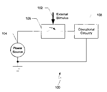
FIG. 1 depicts a high-level schematic of an electronic device configured to
require exposure to an external stimulus for its power-up sequence to proceed.
FIG. 2 depicts a high-level schematic of an electronic device configured to
be rendered operational as soon as it is exposed to the stimulus.
FIG. 3 depicts a high-level schematic of an electronic device configured with
an on/off switch connected in series with a stimulus-sensitive switch.
FIG. 4 is a more detailed schematic depiction of one embodiment of the
invention shown in FIG. 3.
FIG. 5 depicts a high-level schematic of an electronic device, according to
yet another embodiment of the present invention.
FIG. 6 depicts a high-level schematic of an electronic device 100, according
to yet another embodiment of the present invention.
FIG. 7 depicts a sequence of instructions that may be executed by an
embedded processor within the device, according to one embodiment of the
present
invention.
FIG. 8 depicts a system that employs embodiments of the device depicted in
FIGS. 1-7.
FIG. 9 depicts a high-level schematic of a two-way radio, in which
exemplary points for introduction of a stimulus-dependent switch are
identified.
Detailed Description
Theft of portable electronic devices, such as two-way radios, may be deterred
by rendering their power-up sequences dependent upon initial exposure to a pre-
determined stimulus. For example, a two-way radio may be designed to possess a
stimulus-sensitive switch, such as a hall-effect switch, that remains open
until initial
exposure to a given stimulus. By inserting that switch in a circuit critical
to the
operation of the two-way radio (in between the radio's battery and the rest of
its
circuitry, or in series with the radio's speaker, antenna, microphone, or
voltage
regulator, for example), the radio is inoperative until. it is exposed to the
stimulus.
3
CA 02414747 2002-12-19
The stimulus-sensitive switch may be composed of more than one switch, and may
be arranged so that it remains closed (until powering down of the device)
after a
single, brief exposure to the stimulus. Accordingly, per such a scheme, after
a radio
has been turned off, it cannot properly function until it is turned on and
brought to
the source of the stimulus for exposure thereto. By providing the source of
stimulus
only within the confines of the locality in which the radios are to operate,
motivation
to steal the radios is eliminated, because, once powered down, the radios will
not
function until returned to the locality for exposure to the stimulus.
Rendering of a power-up sequence dependent upon exposure to a stimulus
need not be accomplished with a switch. Other approaches exist, such as
programming the device to enter an inactive state, upon powering up; the
device
remains in the inactive state, until initial exposure to the stimulus. Of
course, if the
device is controlled with an application-specific integrated circuit (ASIC),
rather
than with a processor, the ASIC may be designed with such functionality hard-
wired
therein. Once again, by providing the source of stimulus only within the
confines of
the locality in which the radios are to operate, motivation to steal the
radios is
eliminated, because, once powered down, the radios will not function until
returned
to the locality for exposure to the stimulus.
FIG. 1 depicts a high-level schematic of an electronic device 100 configured
to require exposure to an external stimulus 102 for its power-up sequence to
proceed. The electronic device 100 consists of a power source 104, a stimulus-
sensitive switch 106, and operational circuitry 108. The power source 104
provides
electrical current to the operational circuitry 108, so that the device 100
can
function. The operational circuitry 108 includes all of the circuitry required
for the
device 100 to operate. For example, in the case of a two-way radio, the
operational
circuitry 108 may include transmission, reception, and control circuitry,
including
amplification, modulation, demodulation, and filtering circuits. For a given
electronic device 100, the circuits 108 required for operation of the device
100 are
known in the art and need not be recited herein, as their precise design
generally
falls outside of the scope of the present invention.
As can be seen from FIG. 1, the device 100 cannot operate unless the
stimulus-sensitive switch 106 is closed (while the switch 106 is open, the
operational circuitry 108 is deprived of electrical current). The stimulus-
sensitive
switch 106 may have many embodiments. For example, the switch 106 may be
arranged to close if and only if it is exposed to the given stimulus 102.
Thus, for the
device 100 to be operational, the device 100 would have to be in the presence
of the
stimulus 102 at all times. Alternatively, the switch 1.06 may be configured to
close
and remain closed upon an initial exposure to the stimulus 102. Per such an
4
CA 02414747 2002-12-19
embodiment, the device 100 would be rendered operational as soon as it was
exposed to the stimulus 102, and it would remain operational until it was
powered
down.
The stimulus-sensitive switch 106 may be used in conjunction with an on/off
switch (not depicted in FIG. 1; see FIG. 3 for an example of an on/off switch
wired
in series with a stimulus-sensitive switch 106). The on/off switch may be
wired in
series with the stimulus-sensitive switch 106, so that powering up of the
device 100
requires both manually actuating the on/off switch, and exposing the device
100 to
the stimulus 102. Alternatively, the stimulus-sensitive switch 106 may stand
alone,
so that the device commences its power-up sequence as soon as it is exposed to
the
stimulus 102. Such a device 100 could be powered down by manual actuation of
an
off switch (not depicted in FIG. 1).
Various forms of stimuli 102 may be used to activate the switch 106. For
example, the stimulus-sensitive switch 106 may be a hall-effect switch, which
closes
in response to immersion in a magnetic field. In such a case, the stimulus 102
is a
magnetic field. Other forms of stimulus may be used, as well. For example, the
stimulus 102 may be a radio frequency (RF) transmission, an infrared (IR)
transmission, a pulsed magnetic field, or any other form of transmittable
energy.
Additionally, the switch 106 may require an identification code to be
modulated
with the RF, IR, or pulsed magnetic transmission, in order for it to close.
FIG. 2 depicts a high-level schematic of an electronic device 100 configured
to be rendered operational as soon as it is exposed to the stimulus 102. The
device
depicted in FIG. 2 remains operational thereafter, until it has been powered
down.
As shown in FIG. 2, the stimulus-sensitive switch includes more than one
switch 108 and 110. Per the embodiment shown in FIG. 2, a first switch 108 is
configured to close in response to exposure to the stimulus 102. Closure of
the
switch 108 permits electrical current to pass through the switch 108 and into
a
disjunctive summing circuit 112. The disjunctive summing circuit 112 provides
an
output signal, if and only if one of its inputs is asserted. Thus, closure of
the first
switch 108 results in an output from the summing circuit 112, which, in turn,
results
in closure of the second switch 110. Closure of the second switch 110 has two
effects. First, electrical current is allowed to flow to the operational
circuitry 108 of
the device 100, so the device is rendered operational. Second, electrical
current is
fed back into a second input of the disjunctive summing circuit 112, thereby
producing an output therefrom, and thereby causing the second switch 110 to
remain
closed. Accordingly, the stimulus-sensitive switch 106 depicted in FIG. 2
remains
closed after a single, brief exposure to the stimulus 102. Consequently, the
device
100 remains operational thereafter, until such time as it is powered down.
CA 02414747 2002-12-19
FIG. 3 depicts a high-level schematic of an electronic device 100 configured
with an on/off switch 114 connected in series with the stimulus-sensitive
switch 106.
Powering up of this device 100 requires two actions. First, the on/off switch
114
must be manually actuated to the "on" position. Second, the device 100 must be
exposed, for a single, brief period to the stimulus 102. Thereafter, current
flows as
described in the embodiment of FIG. 2, and the device 100 remains operational,
until it is powered down. Per this embodiment, the device 100 may be powered
down by manual actuation of the on/off switch 114 to the "off' position.
FIG. 4 is a more detailed schematic depiction of one embodiment of the
invention shown in FIG. 3. As in FIG. 3, the power source 104, stimulus-
sensitive
switch 106, operational circuitry 108, and onloff switch 114 are connected in
series.
In this embodiment, the stimulus-sensitive switch 106 is designed to remain
closed
after an initial, brief exposure to the stimulus 102.
As shown in FIG. 4, the stimulus-sensitive switch 106 includes a hall-effect
switch 400. The hall-effect switch 400 contains three pins: inputs 400a and
400b,
and output 400c. When immersed in a magnetic field, the hall-effect switch 400
closes, so that inputs 400a and 400b are connected 1:o output 400c. Thus, when
closed, current flows through the switch 400, through the output pin 400c, and
to an
input pin 402a of integrated circuit 402. The integrated circuit 402 is a
single chip
containing three field effect transistors (FETs), two of which are shown in
FIG. 4.
The input pin 402a is connected to the gate of each FET 404 and 406 within the
integrated circuit 402. The power supply 104 is coupled to the source of each
FET
404 and 406, through input pins 402b and 402c. Thus, when the hall-effect
switch
400 is immersed in a magnetic field, a voltage is developed on the gate of
each FET
404 and 406. Consequently, a conduction path within each FET 404 and 406 is
created, permitting current to flow through each FET 404 and 406 and to the
operational circuitry 108, via output pins 402d and 402e (which are connected
to the
drains of the FETs 404 and 406). A second consequence of current flowing
through
the FETs 404 and 406 is that the current is permitted to flow back through the
diode
412, returning to the input pin 402a, thereby keeping both FETs "on." The
resistors
414 and 416 cooperate to form a voltage divider, ensuring that the voltage
present at
input pin 402a exceeds the threshold voltage of the FETs, so that they will be
kept
"on." Capacitors 408, 418, and 410 are connected between ground and the gates,
sources and drains of the FETs 404 and 406 for the purpose of suppressing
transient
effects.
Although the embodiment depicted in FIG. 4 shows two FETs 404 and 406
connected in parallel as the means of passing currenl; to the operational
circuitry 108,
any number of FETs rnay be connected in parallel to accomplish this task (the
6
CA 02414747 2002-12-19
greater the number of FETs connected in parallel, the greater the total
current
delivering capacity). Furthermore, other forms of switches may be used in
place of
the FETs 404 and 406, including switches made from more than one FET, switches
made from a single bipolar junction transistor (BJT), or switches made from
multiple BJTs.
FIG. 5 depicts a high-level schematic of an electronic device 100, according
to yet another embodiment of the present invention. As in previous
embodiments,
the power source 104, stimulus-sensitive switch 106, operational circuitry
108, and
on/off switch 114 are connected in series. In this embodiment, the stirnulus-
sensitive switch 106 is designed to remain closed after an initial, brief
exposure to
the stimulus 102.
The stimulus-sensitive switch 106 of FIG. 5 is composed of a first switch
500, a microprocessor 502, and a second switch 504. When the first switch 500
is
exposed to the stimulus 102, the switch 500 closes, thereby permitting current
to
pass to the microprocessor 502. In response to having received the current,
the
microprocessor 502 may be programmed to deliver an output signal to the second
switch 504, causing that switch 504 to close. Because the second switch 504 is
interposed between the power source 104 and the remainder of the
device°s circuitry
108, the remainder of the circuitry 108 is supplied with power, thereby
permitting
proper operation of the device 100.
One skilled in the art understands that the interface between the first switch
500 and the microprocessor 502 may involve signal-conditioning circuits (level
shifters and the like), which are known in the art. T:he interface may be
accomplished through connection with an input port of the microprocessor 502.
Similarly, one skilled in the art understands that the interface between the
microprocessor 502 and the second switch 504 may take place via an output
port,
and may involve use of a driving circuit for generating the proper
voltage/amperage
to close the switch 504.
Optionally, the microprocessor 502 may be programmed to require a pre-
determined sequence of input pulses before commanding the second switch 504 to
close. For example, the first switch 102 may be a hall-effect switch, which
closes in
response to immersion in a magnetic field. The microprocessor 502 may require
the
magnetic field to be pulsed in a predetermined sequence, before commanding the
second switch 504 to close. Thus, per such an embodiment, a coded stimulus 102
may be implemented for activating the device 100.
One skilled in the art understands that the microprocessor 502 may be
embodied as an ASIC that is hardwired to perform the above-described
functionality.
7
CA 02414747 2002-12-19
FIG. 6 depicts a high-level schematic of an electronic device 100, according
to yet another embodiment of the present invention. As in previous
embodiments,
the power source 104, stimulus-sensitive switch 106, operational circuitry
108, and
on/off switch 114 are connected in series. In this embodiment, the stimulus-
sensitive switch 106 is designed to remain closed after an initial, brief
exposure to
the stimulus 102.
The stimulus-sensitive switch 106 of FIG. 6 is composed of reception
circuitry 600 coupled to a microprocessor 502 that is interfaced with a switch
602.
The switch 602 is interposed between the power source 104 and the remainder of
the
device's circuitry 108. The reception circuitry 600 may include an antenna,
demodulation/recovery circuitry, filtering circuitry, and interface circuitry
(such as
an analog-to-digital converter) to permit the received data to be communicated
to the
processor 502. Such circuitry is known in the art and requires no further
explanation. The microprocessor 502 may be programmed to await a particular
stimulus signal 102 before commanding the switch 602 to close (thereby
providing
electrical current to the remainder of the circuitry 108). For example, the
stimulus
102 may be an IR or RF signal upon which a specific code is modulated. In such
a
case, the reception circuitry 600 demodulates the received stimulus 102 and
communicates the recovered code to the microprocessor 502. The microprocessor
502 may be programmed to await reception of a certain code (such as a code
identifying the particular device) before commanding the switch 602 to close.
Thus,
each device (such as a two-way radio) may have an identification code stored
in
memory; the microprocessor 502 does not close the second switch 602 until
receiving a code that matches the particular identification code stored in
memory.
FIG. 7 depicts a sequence of instructions 700 which may be executed by an
embedded processor within the device 100, according to one embodiment of the
present invention. According to this embodiment, the device 100 includes an
embedded processor that controls the operation of the device 100. The
processor
referred to may be the microprocessor 502 depicted in FIGS. 5 and 6, or may be
included as part of the operational circuitry 108 depicted in FIGS. 1-6.
As can be seen from FIG. 7, upon power up, the embedded processor may be
programmed to enter an inactive state 702, in which the processor is dormant
until
reception of the stimulus 102 is announced to the processor. In query
operation 704,
the microprocessor determines whether the stimulus 102 has been received. If
not,
the microprocessor returns to its inactive state 702. If, on the other hand,
the
stimulus 102 has been received, the processor is permitted to execute the
remainder
of the software/firmware 706 required for normal operation of the device 100.
Accordingly, the device is rendered non-functional until a brief, initial
exposure to
8
CA 02414747 2002-12-19
the stimulus 102. Thereafter, the device 100 remains functional, until powered
down.
FIG. 8 depicts a system 800 that employs embodiments of the device 100
depicted in FIGS. 1-7. The system 800 includes a locality 802 in which the
electronic devices 804, 806, and 808 are to operate. For example, the locality
802
may be a retail space or a warehouse. The system 800 discourages removal of
the
devices 804, 806, and 808 from the locality 802. Further included in the
system 800
is a stimulus source 810, which provides a stimulus 102 that is used to permit
the
various devices 804, 806, and 808 to operate properly after having been
powered
down. The devices 804, 806, and 808 may be designed according to the
embodiments depicted according to FIGS. 1-7.
The stimulus source 810 produces a stimulus 102 used to activate the devices
804, 806, and 808, as discussed throughout the application. The stimulus 102
may
take the form of an electromagnetic signal that propagates through space. If
so, the
signal should be confined to extend not further than a region of space
approximately
coextensive with the locality 802 in which the devices 804, 806, and 808 are
to
operate. Alternatively, the stimulus source 810 may be designed to transmit
such a
stimulus 102 in a region of space 814 immediately surrounding the source 810.
As a
third alternative, the stimulus 102 may be confined to a region of space 812
within
the source 810, itself. Per such an embodiment, a device 804, 806, and 808 is
partially inserted into the source 810 for exposure to the stimulus 102.
As described earlier, the system 800 eliminates the motivation to steal the
devices 804, 806, and 808, because, once powered down, the devices 804, 806,
and
808 must be brought to the stimulus source 810 to be rendered operational.
FIG. 9 depicts a high-level schematic of a two-way radio 900, in which
exemplary points 918a-h for introduction of a stimulus-dependent switch 106
are
identified.
The radio 900 includes a power source 902, such as a battery or battery pack,
coupled to a voltage regulator 906 through an on/off switch 904. The voltage
regulator maintains a particular voltage on power lines within the radio 900.
For
example, digital logic oftentimes runs off of five-volt power lines. Thus, the
voltage
regulator 906 may be designed to yield a five-volt output, with which the
circuitry
within the radio 900 is powered. In the particular embodiment depicted in FIG.
9,
the voltage regulator 906 provides power to a processor 908 and to
transmission/reception/synthesizing circuitry 910.
The processor 908 provides general control for the two-way radio, and is an
exemplary site for execution of the method described with reference to FIG. 7.
The
processor 908 controls such features as the frequency of transmission and/or
the
9
CA 02414747 2002-12-19
introduction sub-audible tones into the transmission stream. As can be seen
from
FIG. 9, the processor 908 communicates data to the transrnission/reception/
synthesizing circuitry 910, which operates based upon the data received
therefrom.
For example, the transmission/reception/synthesizirig circuitry 910 generates
a
carrier frequency and modulates voice data against that frequency, based upon
data
from the processor 908.
The transmission/reception/synthesizing circuitry 910 generally performs the
tasks necessary for transmission and reception of a radio signal, including
production of a carrier signal, modulation, demodulation, amplification, and
filtering
of transmission and reception signals. The transmissionlreception/synthesizing
circuitry 910 is coupled to: (1) a microphone 912 for reception of voice data
to be
modulated against the carrier signal; (2) a speaker 914 for transducing the
received
and demodulated reception signal into a sound signal; and (3) an antenna 916
for
reception and transmission of radio signals.
Broadly speaking, a stimulus-sensitive switch 106 may be interposed in any
operation-critical path in a two-way radio 900 (or any other device, for that
matter).
Such operation-critical sites include, but are not limited to: placement in
series with
the voltage regulator 906, as shown by reference numerals 918a and 918b;
placement in series with the power supply lines for the
transmission/reception/
synthesizing circuitry 910 or the processor 908, as shown by reference
numerals
918d and 918c, respectively; placement in series with the speaker, as shown by
reference numeral 918e; placement in series with the microphone 912, as shown
by
reference numeral 918f; placement in series with the antenna, as shown by
reference
numeral 918g; or placement in series in the data path between the processor
908 and
the transmission/reception/synthesizing circuitry 910, as shown by reference
numeral 918h.
It will be clear that the present invention is well adapted to attain the ends
and advantages mentioned as well as those inherent therein. While presently
preferred embodiments have been described for purposes of this disclosure,
various
changes and modifications may be made which are well within the scope of the
present invention. For example, the system and devices disclosed herein may
utilize any form of stimulus suitable for effective transmission.
Additionally,
transmission of the stimulus itself may be rendered conditional on an event,
such as
identification of the particular electronic device to which the source is to
transmit the
stimulus (for example, the electronic device may be outfitted with an RF
identification tag that permits the source to identify 'the particular
device). Per such
a modification, the source would transmit the stimulus only if the
identification code
contained in the RF identification tag was found in a list of approved
identification
CA 02414747 2002-12-19
codes. One skilled in the art recognizes that the invention disclosed herein
can be
used in conjunction with any portable electronic device, including, but not
limited
to, cordless telephones, cellular telephones or handheld scanners. Numerous
other
changes may be made which will readily suggest themselves to those skilled in
the
art and which are encompassed in the spirit of the invention disclosed and as
defined
in the appended claims.
11