Note: Descriptions are shown in the official language in which they were submitted.
CA 02415689 2006-10-31
1
INK JET PRINTHEAD WITH BLANCED ENERGY SUPPLY AT RESISTIVE
ELEMENTS BY ADAPTED FET-CIRCUITS
BACKGROUND OF THE INVENTION
The subject invention generally relates to ink jet
printing, and more particularly to a thin film ink jet printhead
having FET drive circuits configured to compensate for parasitic
power dissipation along a ground bus.
The art of ink jet printing is relatively well developed.
Commercial products such as computer printers, graphics
plotters, and facsimile machines have been implemented with ink
jet technology for producing printed media. The contributions of
Hewlett-Packard Company to ink jet technology are described, for
example, in various articles in the Hewlett-Packard Journal,
Vol. 36, No. 5 (May 1985); Vol. 39, No. 5 (October 1988); Vol.
43, No. 4 (August 1992) ; Vol. 43, No. 6 (December 1992); and
Vol. 45, No.1 (February 1994).
Generally, an ink jet image is formed pursuant to precise
placement on a print medium of ink drops emitted by an ink drop
generating device known as an ink jet printhead. Typically, an
ink jet printhead is supported on a movable print carriage that
traverses over the surface of the print medium and is controlled
to eject drops of ink at appropr:Late times pursuant to command
of a microcomputer or other controller, wherein the timing of
the application of the ink drops is intended to correspond to a
pattern of pixels of the image being printed.
A typical Hewlett-Packard ink jet printhead includes an
array of precisely formed nozzles in an orifice plate that is
attached to an ink barrier layer which in turn is attached to a
thin film substructure that implements ink firing heater
resistors and apparatus for enabling the resistors. The ink
barrier layer defines ink channels including ink chambers
disposed over associated ink firing resistors, and the nozzles
in the orifice plate are aligned with associated ink chambers.
CA 02415689 2006-10-31
2
Ink drop generator regions are formed by the ink chambers and
portions of the thin film subst:ructure and the orifice plate
that are adjacent the ink chambers.
The thin film substructure is typically comprised of a
substrate such as silicon on which are formed various thin film
layers that form thin film ink firing resistors, apparatus for
enabling the resistors, and also interconnections to bonding
pads that are provided for external electrical connections to
the printhead. The ink barrier layer is typically a polymer
material that is laminated as a dry film to the thin film
substructure, and is designed to bephotodefinable and both W and
thermally curable. In an ink jet printhead of a slot feed
design, ink is fed from one or more ink reservoirs to the
various ink chambers through one or more ink feed slots formed
in the substrate.
An example of the physica:l arrangement of the orifice
plate, ink barrier layer, and thin film substructure is
illustrated at page 44 of the Hewlett-Packard Journal of
February 1994, cited above. Further examples of ink jet
printheads are set forth in commonly assigned U. S. Patent
4,719,477 and U. S. Patent 5,317,346.
Considerations with thin film ink jet printheads include
the need to insure that each of the heater resistors fires an
ink drop when selected. Due to variation in the power
dissipating parasitic resistance presented by the conductive
traces leading between the heater resistors and power and ground
contact pads, the ink firing signals provided to the heater
resistors typically include a cert.ain amount of overenergy. This
means that some resistors ultimately receive more than enough
energy to a fire an ink drop while others receive only enough
energy to fire an ink drop. Excessive energy has various
negative effects including reduced resistor life, "kogation"
which is the accumulation of a ink components that are
tenaciously adhered to the passivation layer in the ink
chambers, and reduced printhead reliability. Also, application
CA 02415689 2006-10-31
3
of different energies to different resistors results in
inconsistent bubble nucleation and drop formation.
While trace width variation is a known technique for
energy balancing, use of such technique makes it difficult to
reduce the width of the thin film substructure of the printhead.
There is accordingly a need for an improved ink jet
printhead wherein heater resistors are more uniformly energized.
SUMMARY OF THE INVENTION
The disclosed invention .Ls directed to an ink jet
printhead having heater resistor energizing FET drive circuits
that are configured to compensate for variation in power trace
parasitic resistances, so as to reduce the variation in the
energy provided to the heater resistors of the printhead.
Accordingly, in one aspect of the present invention there
is provided an ink jet printhead comprising:
a printhead structure formed of a substrate and a
plurality of thin film layers, said print head structure having
a longitudinal extent and longitudinally separated ends;
a longitudinal array of ink drop generators defined in
said printhead structure and aligned with said printhead
longitudinal extent;
bond pads;
a longitudinal array of FET circuits formed in said
printhead structure adjacent said ink drop generators and
aligned with said printhead longitudinal extent;
power traces electrically connected between (a) said bond
pads and (b) said ink drop generators and said FET circuits; and
wherein said FET circuits are respectively configured to
compensate for variation in parasitic resistance presented by
said power traces.
BRIEF DESCRIPTION OF THE DRAWINGS
The advantages and features of the disclosed invention
will readily be appreciated by persons skilled in the art from
CA 02415689 2006-10-31
3a
the following detailed description when read in conjunction with
the drawing wherein:
FIG. 1 is an unscaled schematic top plan view illustration
of the layout of an ink jet printhead that employs the
invention.
FIG. 2 is a schematic, partially broken away perspective
view of the ink jet printhead of FIG. 1.
FIG. 3 is an unscaled schematic partial top plan
illustration of the ink jet printhead of FIG.1.
FIG. 4 is a partial top plan view generally illustrating
the layout of an FET drive circuit array and an associated
ground bus of the printhead of FIG. 1.
CA 02415689 2003-01-21
WO 02/07980 PCT/US01/02647
4
FIG. 5 is an electrical circuit schematic depicting the
electrical connections of a heater resistor and an FET drive
circuit of the printhead of FIG. 1.
FIG. 6 is a plan view of representative FET drive circuits
and the associated ground bus of the printhead of FIG. 1.
FIG. 7 is an elevational cross sectional view of a
representative FET drive circuit of the printhead of FIG. 1.
FIG. 8 is a plan view of plan view depicting an
illustrative implementation of an FET drive circuit array and
associated ground bus of the printhead of FIG. 1.
FIG. 9 is an unscaled schematic perspective view of a
printer in which the printhead of the invention can be
employed.
DETAILED DESCRIPTION OF THE DISCLOSURE
In the following detailed description and in the several
figures of the drawing, like elements are identified with like
reference numerals.
Referring now to FIGS. 1 and 2, schematically illustrated
therein is an unscaled schematic perspective view of an ink jet
printhead in which the invention can be employed and which
generally includes (a) a thin film substructure or die 11
comprising a substrate such as silicon and having various thin
film layers formed thereon, (b) an ink barrier layer 12
disposed on the thin film substructure 11, and (c) an orifice
or nozzle plate 13 laminarly attached to the top of the ink
barrier 12.
The thin film substructure 11 is formed pursuant to
conventional integrated circuit techniques, and includes thin
film heater resistors 56 formed therein. The ink barrier layer
12 is formed of a dry film that is heat and pressure laminated
to the thin film substructure 11 and photodefined to form
therein ink chambers 19 and ink channels 29 which are disposed
over resistor regions in which the heater resistors are formed.
Gold bonding pads 74 engagable for external electrical
CA 02415689 2006-10-31
connections are disposed at longitudinally spaced apart,
opposite ends of the thin film substructure 11 and are not
covered by the ink barrier layer 12. By way of illustrative
example, the barrier layer material comprises an acrylate based
5 photopolymer dry film such as the"Parad"brand photopolymer dry
film obtainable from E. I.duPont de Nemours and Company of
Wilmington, Delaware. Similar dry films include otherduPont
products such as the"Riston"brand dry film and dry films made by
other chemical providers. The orifice plate 13 comprises, for
example, a planar substrate comprised of a polymer material and
in which the orifices are formed by laser ablation, for example
as disclosed in commonly assigned U. S. Patent 5,469,199. The
orifice plate can also comprise a plated metal such as nickel.
As depicted in FIG. 3, the ink chambers 19 in the ink
barrier layer 12 are more particularly disposed over respective
ink firing resistors 56, and each ink chamber 19 is defined by
interconnected edges or walls of a chamber opening formed in the
barrier layer 12. The ink channels 29 are defined by further
openings formed in the barrier layer 12, and are integrally
joined to respective ink firing chambers 19. FIGS. 1, 2 and 3
illustrate by way of example a slot fed ink jet printhead
wherein the ink channels open towards an edge formed by an ink
feed slot in the thin film substructure, whereby the edge of the
ink feed slot forms a feed edge.
The orifice plate 13 includes orifices or nozzles 21
disposed over respective ink chambers 19, such that each ink
firing resistor 56, an associated ink chamber 19, and an
associated orifice 21 are aligned and form an ink drop generator
40.
While the disclosed printhead has been described as having
a barrier layer and a separate orifice plate, it should be
appreciated that the invention can be implemented in printheads
having an integral barrier/orifice structure that can be made
using a single photopolymer layer that is exposed with a
multiple exposure process and then developed.
CA 02415689 2003-01-21
WO 02/07980 PCT/US01/02647
6
The ink drop generators 40 are arranged in three columnar
arrays or groups 61, 62, 63 that are spaced apart from each
other transversely relative to a reference axis L. The heater
resistors 56 of each ink drop generator group are generally
aligned with the reference axis L and have a predetermined
center to center spacing or nozzle pitch P along the reference
axis L. By way of illustrative example, the thin film
substructure is rectangular and opposite edges 51, 52 thereof
are longitudinal edges of the length dimension while
longitudinally spaced apart, opposite edges 53, 54 are of the
width dimension which is less than the length dimension of the
printhead. The longitudinal extent of the thin film
substructure is along the edges 51, 52 which can be parallel
to the reference axis L. In use, the reference axis L can be
aligned with what is generally referred to as the media advance
axis.
While the ink drop generators 40 of each ink drop
generator group are illustrated as being substantially
collinear, it should be appreciated that some of the ink drop
generators 40 of an ink drop generator group can be slightly
off the center line of the column, for example to compensate
for firing delays.
Insofar as each of the ink drop generators 40 includes a
heater resistor 56, the heater resistors are accordingly
arranged in groups or arrays that correspond to the ink drop
generators. For convenience, the heater resistor arrays or
groups will be referred to by the same reference numbers 61,
62, 63.
The thin film substructure 11 of the printhead of FIGS.
1, 2 and 3 more particularly includes ink feed slots 71, 72,
73 that are aligned with the reference axis L, and are spaced
apart from each other transversely relative to a reference axis
L. The ink feed slots 71, 72, 73 respectively feed the ink
drop generator groups 61, 62, 63, and by way of illustrative
example are located on the same side of the ink drop generator
groups that they respectively feed. By way of illustrative
CA 02415689 2003-01-21
WO 02/07980 PCT/US01/02647
7
example, each of the ink feed slots provides ink of a different
color, such as cyan, yellow and magenta.
The thin film substructure 11 further includes drive
transistor circuit arrays 81, 82, 83 formed in the thin film
substructure 11 and located adjacent respective ink drop
generator groups (61, 62, 63) Each drive circuit array (81,
82, 83) includes a plurality of FET drive circuits 85 connected
to respective heater resistors 56. Associated with each drive
circuit array (81, 82, 83) is a ground bus (181, 182, 183) to
which the source terminals of all of the FET drive circuits 85
of the adjacent drive circuit array (81, 82, 83) are
electrically connected. Each ground bus (181, 182, 183) is
electrically interconnected to at least one bond pad 74 at one
end of the printhead structure and to at least one contact pad
74 at the other end of the printhead structure.
As schematically shown in FIG. 5, the drain terminal of
each FET circuit 85 is electrically connected to one terminal
of the adjacent heater resistor 56 which receives at its other
terminal an appropriate ink firing primitive select signal PS
via a conductive trace 86 that is routed to a contact pad 74
at one end of the printhead structure. The conductive traces
86 comprise, for example, traces in a gold metallization layer
that would be above and dielectrically separated from the
metallization layer in which the ground busses 181, 182, 183
are formed. The conductive traces 56 are electrically
connected to the heater resistors 56 by conductive vias and
metal traces 57 (FIG. 6) formed in the same metallization layer
as the ground busses 181, 182, 183. Also, the conductive trace
86 for a particular heater resistor can be generally routed to
a bond pad 74 on the end that is closest to that heater
resistor. Depending upon implementation, the heater resistors
56 of a particular ink drop generator group (61, 62, 63) can
be arranged in a plurality of primitive groups, wherein the ink
drop generators of a particular primitive are switchably
coupled in parallel to the same ink firing primitive select
signal, as for example disclosed in commonly assigned U. S.
CA 02415689 2003-01-21
WO 02/07980 PCT/US01/02647
8
Patents 5,604,519; 5,638,101; and 3,568,171, incorporated
herein by reference. The source terminal of each of the FET
drive circuits is electrically connected to an adjacent
associated ground bus (181, 182, 183).
For ease of reference, the conductive traces including the
conductive trace 86 and the ground bus that electrically
connect a heater resistor 56 and an associated FET drive
circuit 85 to bond pads 74 are collectively referred to as
power traces. Also for ease of reference, the conductive
traces 86 can be referred to as to the high side or non-
grounded power traces.
Generally, the parasitic resistance (or on-resistance) of
each of the FET drive circuits 85 is configured to compensate
for the variation in the parasitic resistance presented to the
different FET drive circuits 85 by the parasitic path formed
by the power traces, so as to reduce the variation in the
energy provided to the heater resistors. In particular, the
power traces form a parasitic path that presents a parasitic
resistance to the FET circuits that varies with location on the
path, and the parasitic resistance of each of the FET drive
circuits 85 is selected so that the combination of the
parasitic resistance of each FET drive circuit 85 and the
parasitic resistance of the power traces as presented to the
FET drive circuit varies only slightly from one ink drop
generator to another. Insofar as the heater resistors 56 are
all of substantially the same resistance, the parasitic
resistance of each FET drive circuit 85 is thus configured to
compensate for the variation of the parasitic resistance of the
associated power traces as presented to the different FET drive
circuits 85. In this manner, to the extent that substantially
equal energies are provided to the bond pads connected to the
power traces, substantially equal energies can be provided to
the different heater resistors 56.
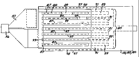
Referring more particularly to FIGS. 6 and 7, each of the
FET drive circuits 85 comprises a plurality of electrically
interconnected drain electrode fingers 87 disposed over drain
CA 02415689 2003-01-21
WO 02/07980 PCT/US01/02647
9
region fingers 89 formed in a silicon substrate 111, and a
plurality of electrically interconnected source electrode
fingers 97 interdigitated or interleaved with the drain
electrodes 87 and disposed over source region fingers 99 formed
in the silicon substrate 111. Polysilicon gate fingers 91 that
are interconnected at respective ends are disposed on a thin
gate oxide layer 93 formed on the silicon,substrate 111. A
phosphosilicate glass layer 95 separates the drain electrodes
87 and the source electrodes 97 from the silicon substrate 111.
A plurality of conductive drain contacts 88 electrically
connect the drain electrodes 87 to the drain regions 89, while
a plurality of conductive source contacts 98 electrically
connect the source electrodes 97 to the source regions 99. By
way of illustrative example, the drain electrodes 87, drain
regions 89, source electrodes 97, source regions 99, and the
polysilicon gate fingers 91 extend substantially orthogonally
or transversely to the reference axis L and to the longitudinal
extent of the ground busses 181, 182, 183. Also, for each FET
circuit 85, the extent of the drain regions 89 and the source
regions 99 transversely to the reference axis L is the same as
extent of the gate fingers transversely to the reference axis
L, as shown in FIG. 6, which defines the extent of the active
regions transversely to the reference axis L. For ease of
reference, the extent of the drain electrode fingers 87, drain
region fingers 89, source electrode fingers 97, source region
fingers 99, and polysilicon gate fingers 91 can be referred to
as the longitudinal extent of such elements insofar as such
elements are long and narrow in a strip-like or finger-like
manner.
By way of illustrative example, the on-resistance of each
of the FET circuits 85 is individually configured by
controlling the longitudinal extent or length of a continuously
non-contacted segment of the drain region fingers, wherein a
continuously non-contacted segment is devoid of electrical
contacts 88. For example, the continuously non-contacted
segments of the drain region fingers can begin at the ends of
CA 02415689 2003-01-21
WO 02/07980 PCT/US01/02647
the drain regions 87 that are furthest from the heater resistor
56. The on-resistance of a particular FET circuit 85 increases
with increasing length of the continuously non-contacted drain
region finger segment, and such length is selected to determine
5 the on-resistance of a particular FET circuit.
As another example, the on-resistance of each FET circuit
85 can be configured by selecting the size of the FET circuit.
For example, the extent of an FET circuit transversely to the
reference axis L can be selected to define the on-resistance.
10 For a typical implementation wherein the power traces for
a particular FET circuit 85 are routed by reasonably direct
paths to bond pads 74 on the closest of the longitudinally
separated ends of the printhead structure, parasitic resistance
increases with distance from the closest end of the printhead,
and the on-resistance of the FET drive circuits 85 is decreased
(making an FET circuit more efficient) with distance from such
closest end, so as to offset the increase in power trace
parasitic resistance. As a specific example, as to
continuously non-contacted drain finger segments of the
respective FET drive circuits 85 that start at the ends of the
drain region fingers that are furthest from the heater
resistors 86, the lengths of such segments are decreased with
distance from the closest one of the longitudinally separated
ends of the printhead structure.
Each ground bus (181, 182, 183) is formed of the same thin
film conductive layer as the drain electrodes 87 and the source
electrodes 97 of the FET circuits 85, and the active areas of
each of the FET circuits comprised of the source and drain
regions 89, 99 and the polysilicon gates 91 advantageously
extend beneath an associated ground bus (181, 182, 183). This
allows the ground bus and FET circuit arrays to occupy narrower
regions which in turn allows for a narrower, and thus less
costly, thin film substructure.
Also, in an implementation wherein the continuously non-
contacted segments of the drain region fingers start at the
ends of the drain region fingers that are furthest from the
CA 02415689 2003-01-21
WO 02/07980 PCT/US01/02647
11
heater resistors 56, the extent of each ground bus (181, 182,
183) transversely or laterally to the reference axis L and
toward the associated heater resistors 56 can be increased as
the length of the continuously non-contacted drain finger
sections is increased, since the drain electrodes do not need
to extend over such continuously non-contacted drain finger
sections. In other words, the width W of a ground bus (181,
182, 183) can be increased by increasing the amount by which
the ground bus overlies the active regions of the FET drive
circuits 85, depending upon the length of the continuously non-
contacted drain region segments. This is achieved without
increasing the width of the region occupied by a ground bus
(181, 182, 183) and its associated FET drive circuit array (81,
82, 83) since the increase is achieved by increasing the amount
of overlap between the ground bus and the active regions of the
FET drive circuits 85. Effectively, at any particular FET
circuit 85, the ground bus can overlap the active region
transversely to the reference axis L by substantially the
length of the non-contacted segments of the drain regions.
For the specific example wherein the continuously non-
contacted drain region segments start. at the ends of the drain
region fingers that are furthest from the heater resistors 56
and wherein the lengths of such continuously non-contacted
drain region segments decrease with distance from the closest
'25 end of the printhead structure, the modulation or variation of
the width of a ground bus (181, 182, 183) with the variation
of the length of the continuously non-contacted drain region
segments provides for a ground bus having a width W that
increases with proximity to the closest end of the printhead
structure,.as depicted in FIG. 8. Since the amount of shared
currents increases with proximity to the bonds pads 74, such
shape advantageously provides for decreased ground bus
resistance with proximity to the bond pads 74.
While the foregoing has been directed to a printhead
having three ink feed slots with ink drop generators disposed
along only one side of an ink feed slot, it should be
CA 02415689 2003-01-21
WO 02/07980 PCT/US01/02647
12
appreciated that the disclosed FET drive circuit array and
ground bus structures can be implemented in variety of slot
fed, edge fed, or combined slot and edge fed configurations.
Also, ink drop generators can be disposed on one or both sides
of an ink feed slot.
Referring now to FIG. 8, set forth therein is a schematic
perspective view of an example of an ink jet printing device
110 in which the above described printheads can be employed.
The ink jet printing device 110 of FIG. 7.includes a chassis
122 surrounded by a housing or enclosure 124, typically of a
molded plastic material. The chassis 122 is formed for example
of sheet metal and includes a vertical panel 122a. Sheets of
print media are individually fed through a print zone 125 by
an adaptive print media handling system 126 that includes a
feed tray 128 for storing print media before printing. The
print media may be any type of suitable printable sheet
material such as paper, card-stock, transparencies, Mylar, and
the like, but for convenience the illustrated embodiments
described as using paper as the print medium. A series of
conventional motor-driven rollers including a drive roller 129
driven by a stepper motor may be used to move print media from
the feed tray 128 into the print zone 125. After printing, the
drive roller 129 drives the printed sheet onto a pair of
retractable output drying wing members 130 which are shown
extended to receive a printed sheet. The wing members 130 hold
the newly printed sheet for a short time above any previously
printed sheets still drying in an output tray 132 before
pivotally retracting to the sides, as shown by curved arrows
133, to drop the newly printed sheet into the output tray 132.
The print media handling system may include a series of
adjustment mechanisms for accommodating different sizes of
print media, including letter, legal, A-4, envelopes, etc.,
such as a sliding length adjustment arm 134 and an envelope
feed slot 135.
The printer of FIG. 9 further includes a printer
controller 136, schematically illustrated as a microprocessor,
CA 02415689 2006-10-31
13
disposed on a printed circuit board 139 supported on the rear
side of the chassis vertical panel 122a. The printer controller
136 receives instructions from a host device such as a personal
computer (not shown) and controls the operation of the printer
including advance of print media through the print zone 125,
movement of a print carriage 140, and application of signals to
the ink drop generators 40.
A print carriage slider rod 138 having a longitudinal axis
parallel to a carriage scan axis _Ls supported by the chassis 122
to sizeably support a print caLrriage 140 for reciprocating
transnational movement or scanninq along the carriage scan axis.
The print carriage 140 supports first and second removable ink
jet printhead cartridges 150,152 (each of which is sometimes
calleda"pen,""print cartridge,"or "cartridge"). The print
cartridges 150,152 include respective printheads 154,156 that
respectively have generally downwardly facing nozzles for
ejecting ink generally downwardly onto a portion of the print
media that is in the print zone 125. The print cartridges
150,152 are more particularly clamped in the print carriage 140
by a latch mechanism that inc:iudes clamping levers, latch
members or lids 170,172.
For reference, print media is advanced through the print
zone 125 along a media axis which is parallel to the tangent to
the portion of the print media that is beneath and traversed by
the nozzles of the cartridges 150,152. If the media axis and the
carriage axis are located on the same plane, as shown in FIG. 9,
they would be perpendicular to each other.
An anti-rotation mechanism on the back of the print
carriage engages a horizontally disposed anti-pivot bar 185 that
is formed integrally with the vertical panel 122a of the chassis
122, for example, to prevent forward pivoting of the print
carriage 140 about the slider rod 138.
CA 02415689 2003-01-21
WO 02/07980 PCT/US01/02647
14
By way of illustrative example, the print cartridge 150
is a monochrome printing cartridge while the print cartridge
152 is a tri-color printing cartridge that employs a printhead
in accordance with the teachings herein.
The print carriage 140 is driven along the slider rod 138
by an endless belt 158 which can be driven in a conventional
manner, and a linear encoder strip 159 is utilized to detect
position of the print carriage 140 along the carriage scan
axis, for example in accordance with conventional techniques.
Although the foregoing has been a description and
illustration of specific embodiments of the invention, various
modifications and changes thereto can be made by persons
skilled in the art without departing from the scope and spirit
of the invention as defined by the following claims.