Note: Descriptions are shown in the official language in which they were submitted.
CA 02415917 2003-O1-08
Application number / numero de demande: ~~/~~~~
Figures:
Pages:
Unscannable items
received with this application
(Request original documents in File Prepo Section on the 1(1h floor)
Documents re~u avec cette demande ne pouvant etre balayes
(Commander les documents originaux Bans la section de preparation des dossiers
au
l0eme etage)
CA 02415917 2003-O1-08
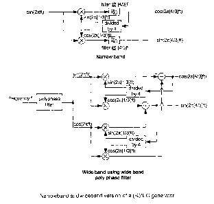
Regenerative Divider Used for Up-Conversion and Down-Conversion
INTRODUCTION
This document describes a form of regenerative dividers that generate the
quadrature components of the carrier frequency required in direct up or down
conversion. The regenerative divider will be incorporated as part of Sirific's
core technology (see PCT patent application serial no. PCTICAOOI00994,
PCTICA00/00995 and PCT/CAOOI00996).
The two regenerative divider circuits are shown in Fig. 1. One is for narrow
band cases and the other is for wide band cases. Both architectures use 3/
the carrier frequency as the local oscillators (LO) - denoted as frequency, f.
The narrow band uses a divided by four element to generate the quadrature
components at a frequency of 1l3 the LO frequency. The two branches (i.e.
the top and bottom) should be as symmetric as possible. It may be
necessary to attach a dummy divided "by 4 element" to the bottom arm to
increase the amount of symmetry. The band-pass filter is centered at 4/3
the LO frequency (or the carrier frequency). This helps remove harmonics
produced by the divided by 4 and the mixers (or multipliers). One of the
harmonics that needs to be removed is the one at 113 the LO frequency.
This harmonic can also be removed using a notch filter centered at 113 LO -
see Fig. 2. In the wide band circuit the 1I3 LO frequency is removed using a
quadrature subtraction technique. The poly phase filter produces
quadrature elements of the LO.
The information contained herein is the exclusive property of SiRil=IC
Wireless Inc. and shall not
be distributed, reproduced, or disclosed without the written permission of
SiRiFIC Wireless inc.
CA 02415917 2003-O1-08
Page 2 of 7 Introduction
fitter @ [413]f
sin(2TCft) cos(2n[4/3]ft)
sin(2~[4/3]ft)
sin(2~cft)_ n
sin(2n[1
b 4 -
frequency,f polyphase ~ cos(2~~[1/3]ft)
filter X -~. sin(2~c[413]ft)
sin(2r~[113]ft)
dwided
by 4
cos(27C[1 /3]ft)
1lliide band using wide band
poly phase vlter
Figure 1: Narrowband andwideband version of a (3/)*LO generator
The information contained herein is the exclusive property of SiRiFIC Wireless
Inc. and shall not
be distributed, reproduced, or disclosed without the written permission of
SiRiFIC Wireless Inc.
filter @ [~./3]f
Narrow band
CA 02415917 2003-O1-08
ChipRF1 Test Plan and Report Page 3 of 7
notch filter
@ [1/3]f
sin(2ltft) -I--r~~(X~------~ .~ ~--T-- cos(2~[413]ft)
sin(2n[413]ft)
notch filter
@ [1l3]f
tJarrow band - using notch filter
Figure 2: Narrow band using a notch filter
In Sirific's down conversion method- see Fig. 3. In this configuration 3/4L0
is used to generate phi_1 - i.e. instead of 2 times the carrier frequency -
one
method has been proposed in the Fig. 4. This figure uses a square wave
to generate phi1 along with XOR gates. The square can be generated from a
frequency controlled oscillator. This square wave may have the ability of
changing frequency and its "digital" pattern - however this waveform has to
have an average value of zero (assuming it is swinging between +1 and -1 ).
I-data
RF
Q-data
General implementation of
using RD within Sirific's core
Figure 3: Using a regenerator divider (RD) within Sirific's core
The information contained herein is the exclusive property of SiRiFIC Wireless
Inc. and shall not
I~e distributed, reproduced, or disclosed without the written permission of
SiRiFIC Wireless Inc.
CA 02415917 2003-O1-08
4 of 7 Architecture Description
I
XOR phi1_I
LO RD square wave
XOR phi1_Q
Q
example of generating phi'I using
RD element
Figure 4: A method of generating phi1_I and phi1_Q using a square wave. The
square wave can be generated using Sirific's "Sogen" block. Sogen can also
generated phi2
ARCHITECTURE DESCRIPTI~N
The version that will be implemented within Silicon is the wide band version
in Figure 1.
The divided by four elements and the mixer configuration will cause the
frequency component at f, to be multiplied with a square wave at frequency
f13. The square waves will be denoted as g_c for the cosine branch and g_s
for the sine branch. Under ideal conditions and ideal matched conditions,
the quadrature summing elements can be represented by the Fig 5.
sin(2~ft)
cos(2~Ft)
Fig. 5: Summing elements with square wave inputs g_c and g_s.
The output is summarized in the table below:
~~ The information contained herein is the exclusive property of SiRiFIC
Wireless lnc. and shall not
be distributed, reproduced, or disclosed without the written permission of
SiRiFIC Wireless Inc.
CA 02415917 2003-O1-08
ChipRF1 Test Plan and Report Page 5 of 7
Table I: Output of Fig. 5, where fund is 413*f
~'; E:; ~r;Pw~'i
~3 ~a r,.
r. 3 ~ ,t~;
52~~' (; '~S, ~ '?3 ;5:.
3 f II fF(S.
d. c, ~ W ~ I~ t
t~ y ~ ' d ~'- ~~ t~
~ Y -. Z ~
,ax2 . :5,~~~"2,~'~~. ... ~ '~.- _E ,;3
r.. M~~ss. ~
r a p v', C :;, 3
~ , 3g
. ~~~ e..Tlf:.:
~ (413)*f fund
3 1/3 0*f DC
1i5 (8/3)*f 2*fund
7 117 (4/3)*f fund
9 1l9 4*f 3*fund
11 1/11 (8I3)*f 2*fund
13 1113 4*f 3*fund
1115 4*f 3*fund
The information contained herein is the exclusive property of SiRiFIC Wireless
Inc. and shall not
be distributed, reproduced, or disclosed without the written permission of
SiRiFIC Wireless Inc.
CA 02415917 2003-O1-08
Page 6 of 7 System Level Design
SYSTEM LEVEL DESIGN
The blocks that need implementing are the following:
1. A linear wide band single to differential converter (range of 525-
1875M Hz)
2. A wide band poly phase filter over a frequency range 525-1875MHz
3. A linear mixer
4. A divided by 4 element
5. XOR block to implement phil_I and phi1_Q
6. Incorporate the sogen block
7. Buffers to drive the LO ports of the mixers
The top-level block diagram is shown in Fig. 6.
"3/4L0" Siggen
and Sogen phi1b_Q
buffers1
phi1 Q
LO in ~ single-diff. ~ Polyphase ~ R.D. ~ xORs
- filter 314 LO
buffersl Philb_I
Soggen phi1_I
Bias phi2b
buffers2 ~ phi2
o cn
..m'ai > > ~i Oi
~i
0
Fig. 6: Top level block diagram of "3/4L0" Siggen and Sogen.
TABLE II: Current estimates and frequency range of components
The information contained herein is the exclusive property of SiRiFIC Wireless
Inc. and shall not
be distributed, reproduced, or disclosed without the written permission of
SiRiFIC Wireless Inc.
CA 02415917 2003-O1-08
ChipRF1 Test Plan and Report Page 7 of 7
~~ The information contained herein is the exclusive property of SiRiFIC
Wireless Inc. and shall not
be distributed, reproduced, or disclosed without the written permission of
SiRiFIC Wireless Inc.
CA 02415917 2003-O1-08
Appendix A
Local Oscillator Generation Scheme
in 0.18 ~m CMOS
for Low-IF and Direct Conversion Architectures
CA 02415917 2003-O1-08
Local Oscillator Generation Scheme in 0.1 ~ ~,m Cl~OS for Low-IF
and Direct Conversion Architectures
Sathwant Dosanjh, William Kung~, Tajinder Manku~, Christopher Snyder~
University of Waterloo, Waterloo, Ontario, N2L 3G1, Canada
~SiRiFIC Wireless Corporation, Waterloo, Ontario, N2J SJ2, Canada
Abstract - A fully-integrated, ratio-based local oscillator products. The LO
system is implemented along with
(LO) generation scheme using regenerative division is direct down-Conversion
mixers to facilitate testing.
described. Using 0.18 IIm CMOS technology, the core LO
system consumes 27 mW from a 1.8 V supply. The entire chip
is fully integrated, including on-chip spiral inductors; II. LO GENERATION
harmonic rejection mixers are also employed to suppress
unwanted mixing products to better than -36 dBc. Across an In (1] and [2], an
offset LO scheme is described
RF band of 150 MHz, a quadrature phase error of less than whereby a 2/3
multiplication factor is used for the GSM
2° and a maximum image suppression of 36 dB is achieved. band and a 4/3
multiplication factor for the DCS/PCS
Using a 4/3 multiplication factor to generate the local bid. For frequency and
phase modulated signals, the
oscillator, LO-1tF interactions are reduced and an LO-RF
leakage of -86 dBm has been measured at the mixer input, down-conversion must
be done in quadrature to retain all
This system can be utilized in low-IF or direct conversion information. Since
the LO is not generated in quadrature,
architectures. a polyphase circuit is inserted in the received RF signal
path; this polyphase would add loss and noise to the
I. INTRODUCTION System [3].
The demand to provide low cost An LO scheme based
wireless solutions has on regenerative division,
also
created much interest in direct utilizing a 4/3 multiplication
conversion architectures. factor, is described
in [4] and
Furthermore, with the long term [5]. The architecture
goal of integrating digital of a system based
on regenerative
processing on-chip, CMOS is the division is shown in
technology of choice. Fig. 1. This architecture
requires a
polyphase filter at
the output to generate
quadrature LO.
Designing a fully-integrated
direct conversion receiver
in CMOS is not without challenges.
In a direct conversion
receiver, the local oscillator tvco ='~ x ~F
operates at the same ~
~e~~
frequency as the received carrier.a~
Thus RF-LO leakage LO = RF~mer
X
can couple to the on-chip voltage
controlled oscillator
(VCO) and degrade receiver performance,
especially in
phase-modulated systems. LO-RF _.
leakage through the 4
substrate can cause LO re-radiation
and produce
undesirable DC offsets. Furthermore,
CMOS technology
offers passive components with Fig. 1. Regenerative
low quality factor and low divider for VCO frequency
at'/a RF~a,,;e~.
self resonant frequencies, which
can pose problems for
the realization of higher frequency
(eg. 5 GHz) designs.
As such, careful LO planning The proposed LO generation
is essential to the design of system, which also
uses
a direct conversion receiver. the technique of regenerative
division [6], provides
quadrature LO signals
(a polyphase filter
at the output is
This paper describes the design not needed) and employs
of a fractional-based harmonic-rejection
mixers
LO generation scheme in a 1.8 (H~) (~]. This architecture
V, 0.18 pm, single-poly, 6- is shown in Fig. 2.
All signal
metal bulk CMOS process for directpaths are fully differential.
conversion or low-IF
architectures. On-chip spiral
inductors and harmonic-
rejection mixers are used to
suppress unwanted mixing
i;
CA 02415917 2003-O1-08
RF'a" based on Gilbert-cell mixers as shown in Fig. 4. The
~,.55-1.70 GNz
phase delayed signals (~~ required by the HRMs are
naturally provided by the divide-by-four circuit. The ~;
signals are weighted and delayed, as described in [7], to
achieve correct harmonic cancellation.
b~~
el~u~k
Qom m. ~'w ~ ~ 4'c,
N ",~--I N ~-iC N
a.~ar n W0. .rzlW.~ ~ WA
'~unpa,~ue i.
~.~.un C~~,
Fig. 4. Circuit diagram ofharmonic-rejection mixer.
Fig.2. System diagram of down-converter using LO
generation scheme. The inputs to the HRM are applied in quadrature to two
sets of HRM pairs. This reduces various mixer products
and also provides quadrature LO outputs. The quadrature
III. LO CIRCUITRY LO signals are applied to a pair of down-conversion
mixers, which provide baseband in-phase and quadrature
A. Polyphase Filter outputs.
The VCO frequency is applied to the fvco port at 3I4
times the RF carrier frequency. A stagger-tuned four-stage IV. MEASURED
RESULTS
polyphase filter is used to generate quadrature signals
from 600 to 1795 MHz. To account for the loss of the A die photo of the
implemented system is shown in Fig.
polyphase filter, it is followed by a gain stage, which 5. The system,
excluding the pad frame, occupies an area
consists of a common-source, differential amplifier. This of approximately 1.5
mm2.
is shown in Fia. 3.
Fig. 3. Circuit diagram of 4-section polyphase filter and gain
stage.
B. Harmonic Rejection Mixers
A divide-by-four circuit is used in feedback with a set
of mixers to generate the 4/3 multiplication factor. A
tuned LC tank forms the load for the HRMs and is used to F'g~ 5. Die photo of
LO generation system and down-
conversion mixers.
suppress the unwanted mixing products generated as a
result of the harmonics produced by the divide-by-four Across an input fvco
range of 1.16 to 1.28 GHz
circuit. An 8.2 nH inductor with a quality factor of 4.5 (equivalent to the
down-conversion of an RF band
was designed, using ASITIC [8). HRMs were employed, between 1.55 to 1.70 GHz),
the measured quadrature
to relax the filtering requirements of the LC tanks The error is shown in Fig.
6. All data is plotted versus the
HRM reduces the mixer products generated by the 3 and fre uenc that was a lied
to the f ort of the chi .
5'" harmonics of the divide-by-four circuit. The HRMs are q y pp vco p p
CA 02415917 2003-O1-08
Quadrature Emor vs. Input fvoo fa Pvco = 0 dBm products were measured to be -
36 dBc, -51 dBe, and -49
2 __..._._...___._._ ________.__.__...____.
_.......______........_._._..__..1.._____........__; dBc, respectively.
1.8 -"
I
t.6 -j , A. Resutts Summary
~ 1.4
9 ' 2 TABLE I
v ' SUMiVIAK'Y OF MEASURED RESULTS
0.6
i
o.e '--i Total power consumptl°n at t.8 V 45 mW
i Core LO arcuit power consumption at 1.6 V 27 mW
0.4 I
RF 6and 1.55 - 1,70 GHz
02 ~ fvcp range required 1.16 - 1.28 GHz
i c i
Quadrature error (P~° -_ p dBm) < 2°
1.16 1.16 1.20 7.22 t.2a 7.26 1.29 Ampiitude mismatch (Pvc" = 0 dBm) < 0.37 dB
I V~(requency =3l4 x RF"""(Gttr) Equivalent Unwanted Image Suppression > 32 d8
LO-RF leakage (0 dBm applied at 1.23 GHZ) -86 dBm at t.fi4 GHz et mixer inputs
RF-LO Leakage (-1o dBm at 7,64 GHz) -72 d8m
Fig. 6. Quadrature error vs. input LO frequency. Harmonic rejection at: t!z x
RF'am", -3s deo
3/2 x RF~,a, -57 dBc
2 x RF'e",~ -49 dHc
Circuit Area (excluding pad frame) t,5 mmz
A quadrature error of less than 2° is achieved over the Ta~hnp~dgy o.te
pm cMOs
enrire frequency range.
Th' id 1 b d ' 1 IF h't t
c
Is A VCO frequency of 3/4 x RF~a,rer,
system or 1.16 to 1.28
cou
a
so
a
use
In
a
ow-
arc
t
ec
ure.
he [iHz, is needed, to operate in
equivalent an RF' band from 1.55 to
unwanted
image
suppression
of
this
down-
onversion 1..70 GHz and generate the required
system LO for direct
has
been
calculated
based
on
the
easured conversion or low-IF architectures.
phase A phase error of less
and
amplitude
mismatch,
and
is
shown
in
ig. than 2, with greater than an
7. equivalent 32 dB image
suppression is achieved across
this band. An LO-RF
ut
d at the mixer in
e
r
l
k
f
86 dB
p
m was m
asu
e
age o
-
ea
Unwanted pp~S. This was achieved m a 1.8
Image V, 0.18 1(,tn, single-poly,
Suppression
vs.
Input
fvco
for
Pvco
=
0
dBm
36.5-~--. _ -.. -----i
j 6-metal bulk CMOS process.
i
36.0
a,
35.5 1
,~ V. CONCLUSION
3s.e
g i
c
3a.5
This paper describes the implementation
of a ratio-
34.0 ~ based LO generation scheme in
a 1.8 V, 0.18 pm, single-
~ poly, 6-metal bulk CMOS process
33.5 for direct conversion or
j --j low-IF architectures. On-chip
33.0 spiral inductors and
32.5 ~ - harmonic-rejection mixers are
used to improve the
32.0 ~ spurious response.
t.16
t.t8
1.20
7.22
t.24
1.28
7.26
,
VCO T
frequency m
= F
3l4
x
RF",mo,
(GFtr)
ACKNOWLEDGEMENT
Fig_ 7. Calculated unwanted image suppression vs. input LO The authors wish to
acknowledge the assistance of T.
frequency. Charania, D. Hoang, B. Hogg, K. Konanur, T. Mantell, D.
As stated, the HRMs are utilized to reduce the mixer Marchesan, S. Walsh, and
G. Weale.
products generated as a result of the 3'd and 5th harmonic
outputs from the divide-by-four circuit. These are situated REFERENCES
at 3/4 x RF~~,.;er and 5/4 x RF°~,;er, and mix with the input 111 A.
Molnar et. al, "A Single Chip Quad Band
LO, at 3/4 x RF~a,~;~r to generate unwanted products at the
(8501900/1800!1900MHz) Direct Conversion GSM/GPRS
following fractions of the RF~a,~;er: 1/2, 3/2, and 2; these RF Transceiver
with Integrated VCOs and Fractional-N
CA 02415917 2003-O1-08
Synthesizer," ISSCC 2002, International Solid-State Circuits [5] J. Strange
and S. Atkinson, "A Direct Conversion
Conference, pp. 184 - 185, Febrnary 2002, San Francisco. Transceiver for Multi-
Band GSM Application," RFIC
Symposium Digest of Papers. pp. 25 - 28, 2000.
[2) R. Magoon and A Molnar, "AF Local Oscillator Path for
GSM Direct Conversion Transceiver with True 50% Duty [6] R. Miller,
"Fractional-Frequency Generators Utilizing
Cycle Divide by Three and Active Third Harmonic Regenerative Modulation,"
Proc. LR.E, vol. 27, pp. 446 -
Cancellation," RFIC Symposium Digest of Papers. pp. 23 - 457, July, L939.
26, 2002.
[7] J. A. Wekion et. al., "A 1.75-GHz Highly Integrated
[3) F. Behbahani et al., "CMOS Mixers and Polyphase Filters Narrow-Band CMOS
Transmitter with Harmonic-Rejection
for Large Image Rejection," IEEE J, Solid-State Circuits, Mixers," IEEE J.
Solid-State Circuits, voh 36, pp. 2003
vol. 36, pp. 873 - 886, June, 2001. 2015, Dec., 2001.
[4] D. Grant, "Solving the Direct Conversion Problem," Planet [8] A. Niknejad
and R. Meyer, "Analysis, Design, and
Analog, Aug., 2001. Optimization of Spiral Inductors and Transformers for RF
IC's," IEEE J. Solid-State Circuits, vol. 33, pp. 1470 -
1481, Oct., 1998.