Note: Descriptions are shown in the official language in which they were submitted.
CA 02416232 2003-O1-14
Doc. No. 23-1 CA Patent
THREE -DIMENSIONAL OPTICAL
AMPLIFIER STRUCTURE
FIELD OF THE INVENTION
[O1] The present invention relates to an optical amplifier; and in particular
to a three-dimensional
optically pumped amplifier structure fox lasers.
BACKGROUND OF THE INVENTION
[02) Production of short pulses with high energy per pulse is usually achieved
by a combination of one
oscillator and one amplifier. The oscillator is traditionally a mode-locked
laser producing very short
pulses, typically less than 100 ps, at high frequency, typically a few tens of
MHz, and with low energy per
pulse, typically a few nJ. To increase the pulse energy to several liJ, one
uses an amplifier working at a
lower repetition rate from a few kHz to a few hundreds of kHz, depending on
the pumping configuration.
These systems are complex and complicated to use because they involve active
modulation (acousto-optic
or electro-optic); high-speed electronics, short-pulse production for the
oscillator, and injection and
synchronization of the pulses inside the amplifier.
[03] Passively Q-switched lasers using Nd-doped crystals can produce high peak
power pulses of
several kVV at a wavelength of 1064 nm. Depending on the experimental setup,
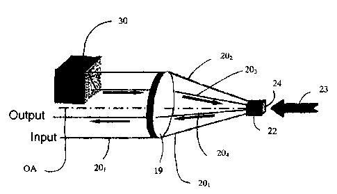
the pulse width can vary
from a few tens of ns (A. Agnesi, S. DeIfAcqua, E: Piccinini, G. Reali and G.
Piccinno, "Efficient
wavelength conversion with high power passively Q-switched diode-pumped
neodymium laser", IEEE, J.
Q. E., Vol. 34, 1480-1484, 1998) to a few hundreds of ps (J. J, Zayhowski,
"Diode-pumped passively Q-
switched picosecond microchip lasers", Opt. Lett., Vol: 19, 1427-1429, 1994).
For example, pulses of 19
ns and 108 ltJ can be obtained at 25 kHz and 1064 nm from a diode-pumped
Nd:YAG laser with a Cr"
:YAG saturable absorber crystal. The high peak power of these lasers allows
efficient wavelength
conversion into the ultra-violet (UV) range with optically nonlinear materials
(A. Agnesi, S. DelfAcqua,
E. Piccinini, G: Reali and G. Piccinno, "Efficient wavelength conversion with
high power passively Q-
switched diode-pumped neodymium laser", IEEE, J. Q. E., Vol. 34, 1480-1484,
1998; J. J. Zayhowski,
"Diode-pumped passively Q-switched picosecond microchip lasers", Opt. Lett.,
Vol. 19, 1427-1429,
1994; J. J. Zaykowski, "UV generation with passively Q-switched microchip
laser", Opt. Lett., Vol. 21,
588-590, 1996).
[04] To reduce the pulse width, while using the same material combination, one
must combine the
active medium and the saturable absorber in a short distance to reduce the
cavity length to about 1 mm. A
CA 02416232 2003-O1-14
Doc. No. 23-1 CA Patent
microchip laser combines the two materials in a monolithic crystal (J. J.
Zaykowski, "Non linear
frequency conversion with passively Q-switched microchip lasers", OLEO 96,
paper CWA6, 23 6-237,
1996) to reduce the energy to approximately 8 p.J at 1064 nm. The two
materials, i.e. the laser material
and the saturable absorber, can be connected by thermal bonding, or the
saturable absorber can be grown
by liquid phase epitaxy (LPE) directly on tlae laser material ($. Ferrand, B.
Chambaz, M. Couchaud,
"Liquid Phase Epitaxy: a versatile technique for the development of miniature
optical components in
single crystal dielectric media", Optical Materials l l; 101, 1998). At the
same time, in order to obtain
sub-nanosecond pulses, the saturable absorber must be highly doped to lower
the repetition rate, e.g. 6-8
kHz with Nd:YAG. The wavelength conversion efficiency from infrared (Ilt) to
UV is in the order of 4
°1o. A solution to simultaneously obtain short pulses and a high
repetition rate is to combine a Nd:YV04
crystal, whose short fluorescence lifetime is well suited for a higher
repetition rate, with a semiconductor-
based saturable absorber in an anti-resonant Fabry-Perot structure (B. Braun,
F. X. Kdarner, G. Zhang, M.
Moser, U. Keller, "56 PS passively Q-switched diode-pumped microchip laser",
Opt. Lett., 22, 381-383,
1997). Unfortunately this structure is nevertheless complex and very difficult
to produce.
[OS] It is therefore difficult to simultaneously produce sub-nanosecond short
pulses, at frequencies of a
few tens of kHz, with several micro-Joule per pulse in a simple and compact
system. Another solution
consists of combining a compact oscillator, producing short pulses at high
frequency, with an amplifier to
increase the pulse energy. Amplifiers have been used in the past with pulsed
microlasers. After
amplification, pulses with 87 nJ (small-signal: gain of 3.5) at 100 kHz have
been produced using a 10-W
diode bar as a pump (C. Larat, M. Schwarz, J. P. Pocholle, G. Feugnet, M.
Papuchon, "High repetition
rate solid-state laser for space communication", SPIE, Vol. 2381, 256-263). A
small-signal gain of 16 has
been obtained with an 88-pass complex structure using two 20-W diode bars as a
pump (J. J. Degnan,
"Optimal design of passively Q-switched microlaser transmitters for satellite
laser ranging", Tenth
International Workshop on Laser Ranging Instrumentation, Shanghai, China, Nov.
11-15, 1996). In these
two examples, the amplification efficiency that can be defined as the ratio
between the small-signal gain
and the pump power is small because the transverse pumping has a low
efficiency due o the poor overlap
of the gain areas with the injected beam. Furthermore, these setups use Nd:YAG
crystals not suited for
high-frequency pulses (the fluorescence lifetime is 230 ~,s).
[06] A combination of Nd ions in two different hosts, in an oscillator-
amplifier system, has been
performed in the past in continuous wave (CW) (H. Plaesmann, S. A. Re, J. J.
Alonis, D. L. Vecht, W. M.
Grossmann; "Multipass diode-pumped solid-state optical amplifier' ; Opt.
Lett., 18, 1420-1422, 1993) or
pulsed mode (C. Larat, M: Schwarz, J. P. Pocholle; G. Feugnet, M. Papuchon,
"High repetition rate solid-
2
CA 02416232 2003-O1-14
Doc. No. 23-1 CA Patent
state laser for space communication", SPIE, Vol. 2381, 256-263). In these
cases, the spectral distance
between the emission lines of the two different materials, i.e. Nd:YAG and
Nd:YV04, limits the srnall-
signal gain to a value lower than that obtained when only Nd:YV04 is used in
both the oscillator and the
amplifier; the aforementioned spectral distance is comprised between 5.5 eni l
and 7.0 cmi' (J. F. Bernard,
E. Mc Cullough, A. J. Alcock, "High gain, diode-pumped Nd:YV04 slab
amplifier", Opt. Commun., Vol.
109, 109-114, 1994).
[07] A number of amplification schemes using Nd ions in crystals have been
studied, but often end up
with complex multipass setups, with low efficiency due to transverse pumping.
[08] End-pumped single-pass or double-pass amplification schemes based on:
guiding structures to
increase the interaction length between the pump beam and the injected beam
have been studied in the
past: in planar guides (D. P. Shepherd, C. T. A. Brown, T. J. Warburton, D. C.
Hanna and A. C. Tropper,
"A diode-pumped, high gain, planar waveguide Nd:Y3 Als 012 amplifier", Appl.
Phys. Left., 71, 876-878,
1997) or in double-cladding fibers (E. Rockat, K. Haroud, R. Dandliker, "High
power Nd-doped fiber
amplifier for coherent intersatellite links", IEEE, JQE; 35, 1419-1423, 1999;
I. Zawischa, K. Plaman, C.
Fallnich, H. Welling, H. Zellner, A. Tunnermann, "All solid-state neodymium
band single frequency
master oscillator fiber power amplifier system emitting 5.5 W of radiation at
1064 nm", Opt. Lett., 24, p.
469-471, 1999), These schemes are; however; not suited for high-peak-power
pulses because unwanted
nonlinear effects, such as the Raman effect, start to appear around 1 kW of
peak power.
[09] A high small-signal gain of 240 was achieved in an end-pumped double-pass
bulk Nd:YLF
amplifier; but it was used with a CW laser with an expensive diode-beam
shaping optical setup (G: J.
Friel, W. A. Clarkson, D. C. Hanna, "High gain Nd:YLF amplifier end-pumped by
a beam shaped bread-
stripe diode laser", CLEO 96, paper CTUL 2$, p. 144; 1996).
[10] US Patent No 6,373,864, Georges et al., issued April 16, 2002 discloses
an entirely passive laser
system both for the generation and amplification of short pulses. In the
Georges et al: invention, the
oscillator directly produces l.tJ pulses at the required repetition rate, and
the pulses are amplified after only
a few passes in a non-synchronized amplifier. The uniqueness of that approach
was to combine an
optically pumped, passively Q-switched, high frequency, NdYAG microchip laser
producing short pulses
with an optically end-pumped Nd:YV04 amplifier producing high small-signal
gain while pumped at low
power. The use of the two materials, Nd:YAG and Nd: YVO~, allowed the best use
of their respective
properties: Nd:YAGlCr4+:YAG microchip lasers are simpler and easier to
manufacture than Nd:YV04
3
CA 02416232 2003-O1-14
Doc. No. 23-1 CA Patent
microchips because they use the same crystal (YAG) for the laser medium and
the saturable absorber, and
can be pioduced in a collective fashion. In addition they produce shorter
pulses except in the case of the
semiconductor saturable absorber described in B. Braun, F. X. Kartner, G.
Zhang, M. Moser, U. Keller,
"56 ps passively Q-switched diode-pumped microchip laser", Opt. Left., 22, 381-
383, 1997: Nd:YV04 is
on the other hand well suited for amplification due to its high stimulated
emission cross section. It is also
better suited than Nd:YAG for higher repetition rates due fo a shorter
fluorescence lifetime (100 ~s
instead of 230 ws)
[ 11~ In the invention disclosed be Georges et al.; the light beam to be
amplified initially gets passed
through the amplifier medium along a first path and subsequently gets
reflected back through the
amplifier medium along a second path, thereby traversing the amplifier medium
twice. The planar
geometry used by Georges et al. is not optimal since the pump beam propagates
in three dimensions
whereas the light beam to be amplified travels in a single plane. This results
in poor overlap between the
volume occupied in the amplifier medium by the pump beam and the volume
occupied in the amplifier
medium by the light beam to be amplified. Georges et al: alludes to mufti-pass
scenarios wherein the
light beam to be amplified traverses the amplifier medium at least twice. Such
mufti-pass amplification
schemes are known. For instance, McIntyre discloses co-linear and two-
dimensional mufti-pass
amplification schemes in US Patent No. 5,268,787, issued December 7, 1993.
Plaessmann et al., in US
Patent No. 5,546,222, issued August 13, 1996 discloses a mufti-pass laser
amplifier that uses optical
focussing between subsequent passes through a single gain medium. The mufti-
pass laser amplification
schemes disclosed by Plaessman et al. are all two-dimensional schemes, i.e.
the mufti-paths of the light
beam traversing the amplifier medium all lie in a same plane. The number of
optical components used in
the embodiments taught by Plaessman et al. is relatively small and
consequently, the alignment of said
components is crucial in view of the mufti-pass amplification scheme.
[12] Three-dimensional amplification schemes are also lrnown. C. LeBlanc et
al., "Compact and
efficient multipass Tiaapphire system for femtosecond chirped-pulse
amplification at the terawatt level",
Optics Letters, Vol. 18, No. 2, Pp. 140-142, January 15, 1993, discloses a
Tiaapphire crystal amplifier
medium pumped at two ends by Nd:YAG light and traversed 8 times by the light
beam to be amplified.
The light beam to be amplified traverses the amplifier medium four times in a
first plane and four other
times in a distinct second plane parallel to the first plane. Another three-
dimensional amplification
scheme is that of Scott et al., "Efficient high-gain laser amplification from
a low-gain amplifier by use of
self imaging multipass geometry", Applied Optics; Vol. 40, No. 15, Pp: 2461-
2467, 20 May 2001. Scott
et al. illustrates how the light beam to be .amplified traverse the amplifier
medium four times in a first
4
' ~ . CA 02416232 2003-O1-14
Doc. No. 23-1 CA Patent
plane and four additional times in a distinct other plane parallel to the
first plane. A phase-conjugate
mirror is then used to double the number of passes.
[13] The three-dimensional amplification schemes discussed above are quite
complex and not well
suited for miniaturization.
SUMMARY OF THE INVENTION
[14] An object of the invention is to provide a method for amplifying a light
beam comprising the step
of passing a light beam through an amplifying medium along multiple paths,
wherein no more than two of
the multiple paths lie in a same plane.
[15] A further object of the invention is to provide an optical amplifier
stage for amplifying a light
beam comprising:
a. a first lens having a collimating end, a focussing end, an optical axis,
and a focal point lying on
the optical axis, the first lens for receiving the light beam at the
collimating end for directing the
light beam towards the focal point along a path s1;
b. an amplifying medium disposed along the optical axis for amplifying the
light beam propagating
along s1;
c. a reflector disposed for reflecting the light beam back through the
amplifier medium towards the
focussing end of the first lens along a path s2 to amplify the light beam,
wherein s1 and s2 lie in a
same plane Pl;
d. N redirecting means {R~, RZ, R3,...,RN}, N being a natural number, disposed
adjacent the
collimating end of the lens;
wherein redirecting means RX, x being a natural number between 1 and N, is for
receiving the
light beam having propagated along the path sue, and for redirecting the light
beam through the first
lens back through the amplifier medium along a path s2X+~ to amplify the light
beam;
wherein, s2X+i and suX+~> lie in a same plane PX+~; and,
wherein all the planes are distinct.
[16] A further object of the invention is to provide an optical amplifier
stage for amplifying a light
beam comprising:
CA 02416232 2003-O1-14
Doc. No. 23-1 CA Patent
a. a lens having a collimating end, a focusing end; an optical axis; and a
focal point lying on the
optical axis, the lens for receiving the light beam at the collimating end,
and for directing the light
beam towards the focal point;
b. an amplifying medium disposed along the optical axis for amplifying the
light beam traveling
therethrough;
c. a reflector for reflecting the light beam back through the amplifying
medium towards the focusing
end of the lens; and
d. at least one reflecting means disposed adjacent the collimating end of the
lens, each reflecting
means for receiving the light beam from the reflector via the amplifying
medium and the lens,
and for reflecting the light back through the lens and the amplifying medium
to the reflector;
wherein each time the light beam passes back and forth between the reflector
and one of the reflecting
means the light beam travels in a different plane through the amplifying
medium.
BRIEF DESCRIPTION OF THE DRAWINGS
[ 17] Fig. l is a schematic illustration of a prior art laser system;
[ 18] Figs. 2a and 2b is a schematic illustration of a prior art optically
pumped amplifier structure;
( 19] Fig. 3 is a schematic illustration of an embodiment of the present
invention; and,
[20] Fig. 4 is a cross-sectional view of an amplifier medium of the embodiment
of Fig. 3;
[21] Fig. 5 is a schematic illustration of an alternative embodiment of the
present invention;
[22] Fig. 6 is a cross-sectional view of an amplifier medium of the embodiment
of Fig. 5;
[23] Figs. 7a and 7b are schematic illustrations of a redirecting means in the
form of a
recirculating fiber; and
[24] Figs. 8a and 8b are schematic illustrations showing the equivalent
performance of a roof
prism compared to two mirrors.
DETAILED DESCRIPTION OF THE INVENTION
[25] Figure 1 depicts a conventional entirely passive laser system for both
the generation and
amplification of short pulses, the full description of which is found in US
Patent No. 6,373,864, issued to
Georges et al. on April 16, 2002: The Georges et al. laser system comprises a
first sub-system; i.e. a
microchip laser stage 1, and a second sub-system; i.e. an amplifier stage 2.
In the microchip laser stage 1,
a first pump laser 3 emits a first pumping radiation 4; which is directed by a
first lens S towards a
microchip laser 6. The microchip laser 6 comprises reflective elements, a
first gain medium and a
saturable absorber, all of which are not depicted. A microchip laser beam 8 is
directed by lenses 7 and 9
6
CA 02416232 2003-O1-14
Doc. No. 23-1 CA Patent
towards an amplifying medium 10 which is optically pumped by a second pump
laser 14, whose pumping
radiation 13 is directed towards the amplifying medium 10 by a lens 12. A
dichroic filter 11, transparent
to pumping radiation 13 and reflective to the microchip laserbeam 8, is
disposed at an end of the
amplifying medium 10. The pumping radiation 13, generated by pump laser 14, is
transmitted through
the dichroic filter 11 and excites the amplifier medium 10, while the
microchip laser beam 8, traversing
the amplifying medium 10 a first time for a first amplification, is reflected
by the dichroic filter 11 back
through the amplifying medium 10 a second time for a second amplification. A
twice-amplified
microchip laser beam 15 is directed by lens 9 town optical circuit (not
shown).
[26] Figures 2a and 2b illustrate the amplifying medium 10 beingpumped by the
pumping radiation
13. Shaded area 16 depicts a cross-sectional view of the volume being
optically pumped by the pumping
radiation 13. It is apparent from figures 2a and 2b that the optically pumped
volume 16 of the amplifying
medium 10 is not being substantially overlapped by the microchip laser beam 8
and the twice-amplified
microchip laser beam 15.
[27] The present invention addresses the poor overlap situation by disclosing
a three-dimensional
amplification scheme that sees the beam to be amplified travel along multiple
paths inside the amplifier
medium with the combined volume occupied by the multiple paths inside the
amplifier medium
substantially overlapping with the volume occupied by the optical pump beam.
This provides a laser
system with high gain and good efficiency.
[28] Figure 3 depicts a preferred embodiment of the present invention. A beam
of light to be
amplified 201 propagates parallel to the optical axis (OA) of a lens 19 and is
directed by the lens 19
towards an amplifier medium 22, which is being optically pumped at a
wavelength 7a,p by a pump beam 23
through a dichroic filter 24 transparent to ~,P. The beam 201, having a
wavelength 7~1, traverses the
amplifier medium 22 for a first time along a first path for a first
amplification and is reflected by the
dichroic filter 24. The reflected beam 202 traverses the amplifier medium a
second time for a second
amplification along a second path and is directed by the lens 19 towards a
reflector in the form of a comer
cube 30. The corner cube 30 displaces the beam 202 into a displaced beam 203
and reflects the beam 20 3
back towards the lens 19, which directs the beam 203 along a third path
towards the amplifier medium 22
for a third amplification. The dichroic filter 24 reflects the beam a second
time and the reflected beam
204 traverses the amplifier medium for a fourth amplification along a fourth
path. Subsequently, the beam
204 is directed towards an output port, preferably via the lens 19. It is
important to note that the plane
defined by the first and second paths and the plane defined by the third and
fourth paths are distinct due to
7
CA 02416232 2003-O1-14
Doc. No. 23-1 CA Patent
the beam-displacing action of the corner cube 30. Having distinct planes imply
that the combined volume
occupied by the beam paths inside the amplifief medium 22 is greater than it
would be were it not for the
presence of the corner cube 30: Figure 4 shows across-sectional view of the
amplifier medium 22 and a
pump beam area 23 populated by areas occupied by the light beam to be
amplified as it propagates along
the first, second, third and fourth paths here labeled by the corresponding
beam numerals 201, 20z, 203 and
204. Although the embodiment just described has the input beam 201 and the
output beam 204 traversing
the lens 19, it is not necessary that they do so for the invention to work.
(29] Figure 5 depicts an alternative embodiment of the present invention. In
Fig. 5, the output pump
beam 34 of a fiber coupled diode array 35 is imaged by a lens 36 on an
amplifier medium 37 through a
dichroic filter 38. A light beam to be amplified 39 propagates along a first
path 40 towards a lens 41,
which directs the beam 39 towards the amplifier medium 37 and the dichroic
filter 38. The dichroic filter
38 reflects the light beam 39 back through the amplifier medium 37 and towards
the lens 41, which
directs beam 39 along a second path 42 to a first roof prism 43. The roof
prism 43 reflects and displaces
the beam 39 to propagate along a third path 44 towards the lens 41, which
directs the beam 39 towards the
amplifier medium 37 and the dichroic filter 38. Again, the dichroic filter 38
reflects the beam 39 for
propagation through the amplifier medium 37 and towards the lens 41, which
directs the beam 39 along a
fourth path 45 to a second roof prism 46. The roof prism 46 reflects and
displaces the beam 39 to
propagate along a fifth path 47 towards the lens 41, which directs beam 39
through the amplifier medium
37 to the dichroic filter 38. Once more, the dichroic filter 38 reflects the
beam 39 through the amplifier
medium 37 and towards the lens 41, which directs the beam 39 along a sixth
path 50 to a third roof prism
51. The roof prism 51 reflects and displaces the beam 39 to propagate along a
seventh path 52 towards
the lens 41, which directs beam 39 through the amplifier medium 37 to dichroic
filter 38. And again, the
dichroic filter 38 reflects the beam 39 for propagation through the amplifier
medium 37 and towards the
lens 41, which directs the beam 39 along an eight path 53 towards an output
port (not shown). The beam
39 is amplified each time it traverses the amplifier medium 37 and
consequently, according to the
description just given, is amplified eight times.
[30] Figure 6 shows a cross-sectional view of the amplifier medium 37 with a
concentric dashed circle
60 representing the area of the cross-section being optically pumped by the
pump beam 34. Also shown in
Fig. 6 are the areas of beam 39 traveling along the various paths 40, 45, 47,
53, 42, 44, 50,: and 52 as they
intercept the cross-section of the pump beam. One can observe in Fig. 6 that
the area covered by beam
paths 40, 4S, 47, 53, 42, 44; 50, and 52 substantially overlap the area 60
covered by the pump beam 34.
8
CA 02416232 2003-O1-14
Doc. No. 23-1 CA Patent
[31] It should be clear to those skilled in the art that the corner cube of
the former embodiment and the
roof prisms of the latter embodiment can be replaced by a number of equivalent
redirecting means. Such
alternative redirecting means include recirculating fiber and mirrors. For
example, Fig. 7a illustrates how
a recirculating fiber 62 can be used to replace the roof prisms or the corner
cube of the previously
described embodiments. In Fig. '7a, a beam of light 60 propagates towards a
lens 74, intersects the lens
74 at a port 72 and is directed along a first path by the lens 74 towards a-
reflector 75. The beam 60 is then
reflected towards the lens 74 along a second path by the reflector 75 and is
directed by the lens 74
towards a first end of a recirculating fiber 6l, said first end located at
port 70. The beam 60 propagates
through the recirculating fiber 61 and exits the recirculating fiber 61 at
port 71. The beam 60 is then
directed along a third path by the lens 74 towards the reflector 75. The beam
60 is then reflected towards
the lens 74 along a fourth path by the reflector 75 and is directed by the
lens 74 towards a port 73. The
beam of light 60 then exits the port 73 as an output beam 62. In Fig. 7a, the
first and second paths form a
first plane, the third and fourth paths form a second plane and the first and
second planes are distinct.
Since Fig. 7a was meant to illustrate how a recirculating fiber can serve as a
redirecting means equivalent
to corner cubes and roof prisms, the amplifier medium present in the
aforementioned embodiments was
left out. Fig. 7b is frontal view of the side of the lens 74 having the ports
70; 71, 72 and 73.
[32] As another example of redirecting means, figures 8a and 8b show how
mirrors can perform the
equivalent task of a roof prism. In Fig. 8a one can see an optical beam 85
entering a roof prism 80 and
being redirected by the roof prism 80. Fig. 8b shows how the two mirrors 81
and 82 perform the same
function as the roof prism 80 on the beam 85: Although not illustrated, one
will understand that a
combination of mirrors can function as a corner cube.
(33] Many types of amplifier medium can be envisaged in the present invention.
Amongst others;
Nd:YV04, Nd:YAG, Yb:YAG, Er:glass and Yb:glass can all be utilized as the
amplifier medium.
[34] It is possible to devise embodiments other than the ones described here
without departing from
the spirit and scope the present invention.
9