Language selection

Search

Patent 2416730 Summary

Third-party information liability

Some of the information on this Web page has been provided by external sources. The Government of Canada is not responsible for the accuracy, reliability or currency of the information supplied by external sources. Users wishing to rely upon this information should consult directly with the source of the information. Content provided by external sources is not subject to official languages, privacy and accessibility requirements.

Claims and Abstract availability

Any discrepancies in the text and image of the Claims and Abstract are due to differing posting times. Text of the Claims and Abstract are posted:

  • At the time the application is open to public inspection;
  • At the time of issue of the patent (grant).
(12) Patent: (11) CA 2416730
(54) English Title: METHOD AND APPARATUS FOR ARC DETECTION AND PROTECTION FOR ELECTRONIC BALLASTS
(54) French Title: PROCEDE ET APPAREIL DE DETECTION A L'ARC ET DE PROTECTION DE REGULATEURS ELECTRONIQUES
Status: Expired and beyond the Period of Reversal
Bibliographic Data
(51) International Patent Classification (IPC):
  • H02M 07/00 (2006.01)
  • H05B 41/28 (2006.01)
  • H05B 41/285 (2006.01)
(72) Inventors :
  • ALEXANDROV, FELIX I. (United States of America)
(73) Owners :
  • OSRAM SYLVANIA INC.
(71) Applicants :
  • OSRAM SYLVANIA INC. (United States of America)
(74) Agent: SMART & BIGGAR LP
(74) Associate agent:
(45) Issued: 2010-06-29
(86) PCT Filing Date: 2001-07-23
(87) Open to Public Inspection: 2002-01-31
Examination requested: 2006-06-20
Availability of licence: N/A
Dedicated to the Public: N/A
(25) Language of filing: English

Patent Cooperation Treaty (PCT): Yes
(86) PCT Filing Number: PCT/US2001/023133
(87) International Publication Number: US2001023133
(85) National Entry: 2003-01-16

(30) Application Priority Data:
Application No. Country/Territory Date
60/220,044 (United States of America) 2000-07-21

Abstracts

English Abstract


An electric arc detection apparatus and method is based on AC current
rectification phenomena in air plasma that causes low frequency amplitude
modulation of high frequency currents and voltages in the ballast when
disconnecting the lamp (Lamp) from the electronic ballast with power applied.
A protection circuit (R25, C27, D44, D45, C28, C27, M4) shuts off the inverter
(M1 and M2) of the ballast so the duration of the arc is diminished so that
the arc becomes almost non-visible. The protection circuit senses the input of
the ballast inverter resonant tank (C3 and L1), which is free of transients
caused by resonance, detecting arc rectification frequency which is about 25-
30 times less than the inverter carrier frequency, and turns on a switching
device (M4) for stopping oscillations in the inverter (M1 and M2). When the
lamp (Lamp) is reconnected to the ballast, it resets the protection circuit
and the ballast inverter restarts automatically.


French Abstract

L'invention concerne un appareil et un procédé de détection à l'arc électrique basés sur un phénomène de rectification du courant CA dans un plasma à air qui provoque une modulation d'amplitude à basse fréquence de courants et tensions haute fréquence dans le régulateur lorsque la lampe (Lampe) est débranchée du régulateur électronique et l'énergie activée. Un circuit de protection (R25, C27, D44, D45, C28, C27, M4) coupe l'inverseur (M1 et M2) du régulateur de manière à diminuer la durée de l'arc et à rendre ce dernier quasi invisible. Le circuit de protection détecte l'entrée du réservoir résonnant (C3 et L1) de l'inverseur du régulateur qui est exempt de phénomènes transitoires causés par résonnance, détecte la fréquence de rectification de l'arc qui est environ 25 à 30 fois inférieure à la fréquence porteuse de l'inverseur, et met en marche un dispositif de commutation (M4) pour arrêter les oscillations dans l'inverseur (M1 et M2). Lorsque la lampe (Lampe) est rebranchée au régulateur, elle remet à zéro le circuit de protection et l'inverseur du régulateur redémarre automatiquement.

Claims

Note: Claims are shown in the official language in which they were submitted.


What is claimed is:
1. An electronic ballast circuit for a lamp with arc detection comprising:
a DC/AC inverter;
a ballast output lamp connector;
a low pass signal filter having an input electrically connected to the DC/AC
inverter;
a rectifier electrically connected to the low pass signal filter;
an energy storage element electrically connected to receive a rectified output
of
the low pass signal filter;
a switching device electrically connected to the energy storage element and to
a
disable terminal of the electronic ballast circuit;
wherein the electronic ballast circuit is configured so that during normal
operation of the lamp, the energy storage element is charged to a voltage less
than a
voltage required to close the switching device, and wherein under a condition
of
electrical arcing from the lamp connector of the electronic ballast, the
energy storage
element is charged to a voltage at least as high as the voltage required to
close the
switching device and activate the disable terminal.
2. The electronic ballast circuit of claim 1, wherein the disable terminal is
connected through a switching transistor disabling diode to a gate of at least
one of the
switching transistors.
3. The electronic ballast circuit of claim 1, wherein the DC/AC inverter
comprises an inverter control circuit, and wherein the disable terminal is
connected
through an inverter control circuit disabling diode to the inverter control
circuit.
4. The electronic ballast circuit of claim 1, wherein the electronic ballast
circuit
further comprises a power factor correction element, the disable terminal
being
connected through a PFC disabling diode to the power factor correction
element.
5. The electronic ballast circuit of claim 1, wherein the low pass signal
filter
comprises a filtering resistor and a filtering capacitor.
8

6. The electronic ballast circuit of claim 1, wherein the rectifier comprises
at least
one diode.
7. The electronic ballast circuit of claim 6, wherein the rectifier comprises
a first
rectifying diode connected in parallel with the filtering capacitor.
8. The electronic ballast circuit of claim 7, wherein the rectifier comprises
a
second rectifying diode electrically connected to the energy storage element.
9. The electronic ballast circuit of claim 8, wherein the first rectifying
diode is a
Zener diode.
10. The electronic ballast circuit of claim 1, wherein the energy storage
element
comprises a storage capacitor.
11. The electronic ballast circuit of claim 1, wherein the switching device
comprises a transistor connected between the output node and ground.
12. The electronic ballast circuit of claim 11, wherein the energy storage
element
is connected to a control terminal of the transistor.
13. The electronic ballast circuit of claim 12, wherein the switching device
is a
FET and the energy storage element is a capacitor connected to a gate of the
FET.
14. The electronic ballast circuit of claim 1, wherein the low pass signal
filter is a
low pass notch signal filter comprising a low frequency block signal filter.
15. The electronic ballast circuit of claim 14, wherein the low frequency
block
signal filter comprises a low frequency block resistor and a low frequency
block
capacitor connected in parallel with one another.
16. An arc detection circuit for an electronic lamp ballast comprising:
an input node;
9

a low pass signal filter electrically connected to the input node;
a rectifier electrically connected to the low pass signal filter;
an energy storage element electrically connected to receive a rectified output
of
the low pass signal filter;
a switching device electrically connected to the energy storage element and to
an
output node;
wherein the arc detection circuit is configured so that when the input node is
connected to an AC output voltage of the electronic lamp ballast during normal
operation
of the lamp, the energy storage element is charged to a voltage less than a
voltage
required to close the switching device, and wherein under a condition of
electrical arcing
from a lamp connector of the electronic ballast, the energy storage element is
charged to
a voltage at least as high as the voltage required to close the switching
device.
17. The arc detection circuit of claim 16, wherein the low pass signal filter
comprises a filtering resistor and a filtering capacitor connected in series
with one
another.
18. The arc detection circuit of claim 16, wherein the rectifier comprises at
least
one diode.
19. The arc detection circuit of claim 18, wherein the rectifier comprises a
first
rectifying diode connected in parallel with the filtering capacitor.
20. The arc detection circuit of claim 19, wherein the rectifier comprises a
second rectifying diode arranged in series with the energy storage element,
the second
rectifying diode and the energy storage element together being connected in
paxallel with
the filtering capacitor.
21. The arc detection circuit of claim 20, wherein the first rectifying diode
is a
Zener diode.
22. The arc detection circuit of claim 16, wherein the energy storage element
comprises a storage capacitor.
10

23. The arc detection circuit of claim 16, wherein the switching device
comprises
a transistor connected between the output node and ground.
24. The arc detection circuit of claim 23, wherein the energy storage element
is
connected to a control terminal of the transistor.
25. The arc detection circuit of claim 24, wherein the switching device is a
FET
and the energy storage element is a capacitor connected to a gate of the FET.
26. The arc detection circuit of claim 16, wherein the low pass signal filter
is a
low pass notch signal filter comprising a low frequency block signal filter.
27. The arc detection circuit of claim 26, wherein the low frequency block
signal
filter comprises a low frequency block resistor and a low frequency block
capacitor
connected in parallel with one another.
28. A method of detecting and stopping an electrical arc from a ballast
connector, wherein a lamp is energized via the ballast connector by a resonant
inverter
including an inverter control circuit controlling switching transistors to
produce an AC
voltage to a series resonant tank in the inverter, the method comprising the
steps of
filtering the AC voltage with a low pass filter to remove AC components at
least
as high as frequency components associated with normal operation of the
inverter;
charging an energy storage element from an output of the low pass filter so
that
the energy storage element is charged to voltage higher than a threshold
voltage if
frequency components of the AC output voltage lower than the frequency
components
associated with normal operation of the inverter are present; and
disabling the inverter if the energy storage element reaches the threshold
voltage.
29. The method of claim 28, wherein the disabling step comprises disabling the
inverter control circuit.
30. The method of claim 28, wherein the disabling step comprises disabling at
least one of the switching transistors.
11

31. The method of claim 28, wherein the inverter is connected to a power
factor
correction unit, and wherein the disabling step comprises disabling the power
factor
correction unit.
32. The method of claim 28, wherein the AC input voltage to the low pass
filter
is taken from an electrical point of the inverter between the switching
transistors and the
series resonant tank circuit.
33. The method of claim 32, wherein the AC voltage is taken from an electrical
point in the inverter between a DC capacitor electrically connected to the
switching
transistors and the series resonant tank circuit.
34. The method of claim 33, wherein the AC voltage is taken from an electrical
point in the inverter connected to both the DC capacitor and an inductor in
the series
resonant tank circuit.
35. A method for detecting an arc from a ballast connector, wherein a lamp is
energized via the ballast connector by a resonant inverter including an
inverter control
circuit controlling switching transistors to produce an AC voltage to a series
resonant
tank in the inverter, the method comprising the steps of:
sensing the AC voltage;
filtering out components of the sensed AC voltage other than low frequency
components corresponding to a rectification frequency of the arc to produce a
filtered
signal;
rectifying said filtered signal;
storing energy of the rectified filtered signal over a plurality of periods;
and
generating an arc detection signal based on the stored energy.
36. The method of claim 35, wherein the AC voltage is taken from an electrical
point in the inverter between the switching transistors and the series
resonant tank circuit
in the inverter.
12

37. The method of claim 36, wherein the AC voltage is taken from an electrical
point in the inverter between a DC capacitor electrically connected to the
switching
transistors and the series resonant tank circuit.
38. The method of claim 37, wherein the AC voltage is taken from an electrical
point in the inverter connected to both the DC capacitor and an inductor in
the series
resonant tank circuit.
13

Description

Note: Descriptions are shown in the official language in which they were submitted.


CA 02416730 2003-O1-16
WO 02/09479 PCT/USO1/23133
Method and Apparatus for Arc Detection and
Protection for Electronic Ballasts
BACKGROUND OF THE INVENTION:
Field of the Invention:
This invention relates to electronic ballasts for powering a high frequency
electrodeless fluorescent lamp. An electric arc appears in the lamp connector
when
disconnecting the lamp under power. It is destructive to the ballast and
dangerous to the
personnel replacing lamps. Also, arcing may be caused by poor connections in
the
fluorescent lamp wiring or disconnecting of crimped wire from the connector
and may
create a fire hazard.
Description of the Related Art:
Since the fluorescent lamp is powered from a current source with high
operating
frequency (250 kHz or more), such as a self oscillating DC to AC inverter, a
stable arc
path is established between connector pins or between the connector pin and a
lamp wire,
even if two separated portions axe placed by a distance of up to 1-2 inches
from each
other. At high frequency, recombination time of particles (electrons and ions)
in arc
plasma becomes comparable with AC frequency. When crossing zero current, it is
not
enough time for particles to be recombined in gas molecules and to stop the
current flow
and cancel the arc. Therefore, it should be done artificially by stopping
oscillation in the
ballast inverter with a shut down circuit susceptible to the arc.
There are a few known drawbacks, however. When the arc appears in the
connector, there is no actual change in ballast high frequency voltages and
currents that
could be used for arc detection, as the voltage drop across the arc is
negligible in relation
to lamp rated voltage. Additionally, there is a large increase in ballast
voltages and
currents during normal lamp starting and they are also effected by low
frequency
100/120 Hz steady-state modulation caused by the AC line rectifier. To avoid
false
responses, the arc detection circuit should not be susceptible to all of these
disturbances,
which occur during normal lamp operation.

CA 02416730 2003-O1-16
WO 02/09479 PCT/USO1/23133
The prior art teaches arc cancellation in the lamp connector by mechanically
interlocking
the ballast inverter when unplugging the lamp. In some ICETRON lENDUR.A
electrodeless lamps, additional pins are used in the connector to disconnected
some
components of the ballast inverter without which oscillations in the inverter
cannot exist.
However, the required three-wire connector is thick, expensive, and not
applicable for a
lamp that is placed a distance from the ballast.
Other references disclose different sensing means for arc detection, but they
are
only associated with low frequency AC devices, like electrical welding
equipment, and
not applicable for an arc in high frequency ballasts. Furthermore, the purpose
of such
devices is arc stability. In contrast, the purpose of the present invention in
a ballast is arc
cancellation.
Therefore, a protection method and circuit with fast arc cancellation
capability is
still needed. Another feature of the protection circuit should be a reset
capability for
restarting a reconnected lamp. The protection circuit is also required in the
event that the
ballast is mistakenly turned on without a lamp.
BRIEF DESCRIPTION OF THE DRAWINGS
Figure la illustrates arc current and ballast output voltage plots in
transition from
regular operation to arc condition caused by unplugging an electrodeless lamp.
Figure 1b illustrates the same parameters as those in Figure la at a point
when
current rectification in the arc is starting.
Figure 2 shows a ballast circuit diagram with a block diagram of an arc
detection
and cancellation circuit of the present invention.
Figure 3 shows a circuit diagram of ballast with a self oscillating inverter
and an
arc cancellation circuit.
Figure 4 shows an arc detection and cancellation circuit with a notch filter.
Figure 5 illustrates arc current and output voltage plots of the ballast with
arc
cancellation, taken when unplugging an electrodeless lamp.
DESCRIPTION OF THE PREFERRED EMBODIMENTS
2

CA 02416730 2003-O1-16
WO 02/09479 PCT/USO1/23133
In Figure la, the upper plot is ballast output voltage Vo"t and the bottom
plot is
ballast output current Iout powering a lamp via a connector when the ballast
is not
provided with arc protection. The left side of the plots represents normal
ballast
operation with a lamp plugged in to the connector, just starting its movement
away from
the connector. It is at the very beginning of arcing, when the gap between
connector pins
is very small, that low voltage can break the gap. As the elements between
which the arc
has formed move further, the current waveform changes. Small steps are evident
in arc
AC current Iout at zero crossings. This represents a beginning of the
recombination
process in plasma. But plasma in the gap still continues breaking in both
directions by
AC output voltage.
As the gap further increases, the recombination process advances, so air-
plasma
mixture in the gap stops breaking in one direction. This is shown by intervals
in which
high frequency current pulses follow randomly in one direction only. Depending
on the
concentration of particles in different spots of plasma, it can be broken in
one direction
and unbroken in the opposite direction. This means that a connector pin may
operate as
a cathode and the opposite pin as an anode, or vise versa. Accordingly, when
the arc
conducts, the ballast resonant capacitor provides extra current to the lamp in
one
direction and when it does not conduct, the capacitor absorbs extra current in
the
opposite direction. Therefore, a low frequency component appeaxs in the output
ballast
voltage Vo"t.
Further, low frequency oscillations create a situation in which higher
absolute
peak voltages are being applied in one direction and lower absolute peak
voltages are
being applied in the opposite direction. Therefore, the air/plasma mixture has
a tendency
of breaking in one direction (rectification effect). The low frequency
oscillations
become relatively stable, as illustrated in Figure 5. This system can be
classified as an
oscillator with negative impedance wherein the air/plasma mixture represents
this
negative impedance.
In the inverter of Figure 2, low frequency amplitude modulation caused by arc
rectification affects almost all voltages and currents in the ballast.
However, these
voltages and currents are inconvenient for axc detection since they are also
affected by
resonance during normal lamp starting. According to the invention, inverter
resonance
3

CA 02416730 2003-O1-16
WO 02/09479 PCT/USO1/23133
tank input voltage Vas (see Figure 2) is utilized for detecting the arc in the
connector,
since this voltage is directly affected by arc rectification and is not
affected by resonance.
The arc detection method is based on detection of the AC rectification
phenomena that characterizes an electrical arc in air-plasma when it is
powered from an
AC current source. The above method comprises steps of generating an arc
through an
air gap as a result of disconnecting the lamp from an operating ballast,
alternatively
rectifying positive and negative ballast voltage pulses by the arc, generating
low
frequency amplitude modulation of the ballast output voltage, sensing input
voltage of
ballast inverter resonant tank, determining a low frequency signal of the
voltage
corresponding to the rectification frequency, filtering out such signal from
all other
signals applied to the resonant tank, rectifying the signal, and holding
energy of the
rectified signal for a few of its periods. This resulting signal is utilized
to shut down the
ballast inverter and cancel the arc.
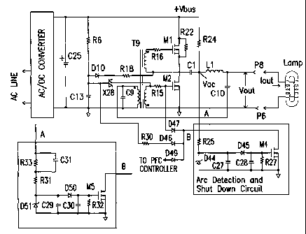
The circuit illustrated in Figure 2 includes elements of a known ballast
circuit
including a DC/AC inverter connected between a DC power source and a lamp
connector. The DC power source may be a rectified AC source, a battery, or any
other
source of DC power.
The DC/AC inverter includes a capacitor C25 connected between common and
DC voltage +Vbus. Also connected between +Vbus and common are switching
transistors M1 and M2. The gates of Ml and M2 are separately connected through
resistors R16 and R15, respectively, to outputs of an inverter control
circuit. The point
between Ml and M2 is connected to a first terminal of DC capacitor C1. A
series
resonant tank circuit is connected between a second terminal of Cl and common.
The series resonant tank circuit includes inductor L1 and capacitor C3. Lamp
connector pins P6~ and P8 are connected to respective terminals of the series
resonant
tank capacitor C3. A feedback circuit is connected between a point between Ll
and C3
in the resonant tank circuit and an input of the inverter control circuit.
These features of a DC/AC inverter are known in the art.
4

CA 02416730 2003-O1-16
WO 02/09479 PCT/USO1/23133
The arc detection and cancellation circuit of the present invention (as
illustrated
in Figure 2) includes a low pass signal filter circuit sensing the voltage Vas
at the input of
the inverter resonant tank designed to select low frequency voltage signal
components
that corresponds to arc rectification frequency, a rectifier connected to the
output of the
filter circuit for rectifying this voltage signal, an energy storage circuit
for holding
energy of these signals, a threshold device for noise immunity, and a latching
switching
device for shut down of the inverter and PFC through a disable terminal via
diodes D47
and D49.
In the embodiment illustrated in Figure 3, a self oscillating inverter is
formed by
switching transistors Ml and M2 driven by a feedback transformer T9, DC
capacitor C1,
and the series resonant tank with inductor L1 and capacitor C3. An
electrodeless Iamp is
connected in parallel to the resonant capacitor C3 through connector pins P6
and P8.
The inverter start circuit comprises a discharge capacitor C13, a diac X28 and
a resistor
R6 connected to positive bus rail +Vbus. DC bus voltage is formed by a boost
type
AC/DC converter. It can be a power factor corrector (PFC), driven by a PFC
controller
(not shown in Figure 3). An arc detection and shut down circuit comprises a
low pass
signal filter (R25, C27), a rectifier of the low frequency signal caused by
the rectification
process in the arc (diodes D44, D45), a storage capacitor C28, a discharge
resistor R27
and, a switching transistor M4.
An advanced arc detection and shut down circuit illustrated in Figure 4
comprises .
a low pass notch filter that is formed as a series combination of a RC low
pass signal
filter (R31, C29) and a low frequency block signal filter (R33, C31). This
circuit has an
input terminal A and an output disable terminal B corresponding to the
terminals with
the same designations of Figure 3. The notch filter is tuned up to pass the
low frequency
signal generated by the electrical arc.
During normal operation of the ballast in Figure 3, high carrier frequency
rectangular voltage Va~ is applied to input A of the arc detection circuit.
This voltage is
filtered out by low pass filter R25/C27. As a result, voltage across capacitor
C27 is well
below a diode drop voltage and has no effect on the input of the transistor
M4. When
arcing occurs and a low frequency rectification begins in the arc, a low
frequency
amplitude modulation is superposed on the high frequency voltage Va~. RC
filter
5

CA 02416730 2003-O1-16
WO 02/09479 PCT/USO1/23133
R25/C27 has a low loss regarding a modulation frequency that is, at Ieast, an
order less
than that of the carrier frequency, so that frequencies associated with normal
lamp
operation are filtered out. As an example, in the case of an ICETRON/ENDUR.A
electrodeless lamp having carrier frequency of about 250 kHz, modulation
frequency in
the arcing connector is in the range of about 8-10 kHz. It creates a low
frequency signal
at the "A" input having a peak to peak voltage of a few tens of volts that is
attenuated by
the filter.
At least a few volts of the low frequency signal is applied across the diode
D44.
In the circuit of Figure 3, for reasons of simplicity only a positive wave of
the signal
charges the capacitor C28 via the diode D44. The negative wave is shorted by
the diode
D44. When voltage across the gate of the transistor M4 reaches the turn-on
threshold of
the transistor, the transistor M4 starts being turned "on" with low frequency.
It creates
more disturbances at the input "A" of the arc detection circuit as well as
higher voltage
across the capacitor C28, and ultimately stops switching of the transistors Ml
and M2.
The capacitor C28 stores voltage that keeps the transistor M4 in the "on"
condition
during the recombination process of electrical particles in plasma. When
impedance in
the air gap changes from low to high, a latching signal from DC bus via the
resistor R24
applies to the input "A" of the arc detection circuit.
The diode D44 can be selected as Zener diode that protects the gate of the
transistor M4 from over voltage. Since Zener diodes have high parasitic
capacitance, the
capacitor C29 can be omitted. The shutdown transistor M4 shorts out the
capacitor C13
through the disable terminal B via a diode D46 and limiting resistor R30,
preventing the
ballast from restarting the inverter after the shutdown. It also shuts off the
PFC
controller (not shown in Figure 3) via a diode D49 and provides a reset
capability. When
the lamp is reconnected, it couples input ~ "A" of the arc detection circuit
to the
"common", the capacitor C28 discharges via the resistor R27, and the shut down
transistor M4 turns off, releasing the PFC controller and the capacitor C13
that charges
and turns on the diac X28.
The operation manner of the arc detection circuit of Figure 4 is similar to
that of
Figure 3. By comparison, the input filter in Figure 4 provides more noise
immunity
against transients generated during the inverter start up and against 100/120
Hz ripple
6

CA 02416730 2003-O1-16
WO 02/09479 PCT/USO1/23133
coming from the AC line. Beyond that, R31 and C29 correspond to the filter
formed by
R25 and C27; D51 and D50 correspond to rectifying diodes D44 and D45; C30
corresponds to storage capacitor C28; R32 corresponds to discharge resistor
R27; and
M5 corresponds to shutdown transistor M4.
The further useful feature of the arc detection and shut down circuit in Fig.3
is its
ability to interlock the ballast start circuit when the ballast'is powered on
without a lamp
connected. This circuit shorts out starting capacitor C13 before it is charged
to the
threshold voltage of diac X28.
As an example of a low cost solution for an ICETRON/ENDUR.A arc detection
and shut down circuit such as that illustrated in Figure 3, the following
components can
be used: R24-1 MSZ; R25 and R27-470 kSZ; C27-1 nF; C28-470 pF; D44-1N5248B;
D45,
D46, and D49-1N4148; D47-IN4005GP; M4-IRFD014. With the above components, it
takes about 5 msec to cancel an arc caused by disconnecting the lamp from the
ballast, as
illustrated in Figure 5. This makes the arc non-visible and not dangerous.
The embodiments described above are intended to be illustrative and not
limiting.
It is recognized that various equivalents, alternatives, and modifications are
possible
within the scope of the appended claims.
7

Representative Drawing
A single figure which represents the drawing illustrating the invention.
Administrative Status

2024-08-01:As part of the Next Generation Patents (NGP) transition, the Canadian Patents Database (CPD) now contains a more detailed Event History, which replicates the Event Log of our new back-office solution.

Please note that "Inactive:" events refers to events no longer in use in our new back-office solution.

For a clearer understanding of the status of the application/patent presented on this page, the site Disclaimer , as well as the definitions for Patent , Event History , Maintenance Fee  and Payment History  should be consulted.

Event History

Description Date
Inactive: IPC expired 2020-01-01
Time Limit for Reversal Expired 2019-07-23
Letter Sent 2018-07-23
Letter Sent 2011-05-19
Grant by Issuance 2010-06-29
Inactive: Cover page published 2010-06-28
Letter Sent 2010-04-27
Amendment After Allowance Requirements Determined Compliant 2010-04-27
Amendment After Allowance (AAA) Received 2010-01-12
Pre-grant 2010-01-12
Inactive: Amendment after Allowance Fee Processed 2010-01-12
Inactive: Final fee received 2010-01-12
Notice of Allowance is Issued 2009-11-20
Letter Sent 2009-11-20
Inactive: Approved for allowance (AFA) 2009-11-04
Letter Sent 2006-08-03
Request for Examination Received 2006-06-20
Request for Examination Requirements Determined Compliant 2006-06-20
All Requirements for Examination Determined Compliant 2006-06-20
Inactive: IPC from MCD 2006-03-12
Inactive: Cover page published 2003-03-28
Inactive: Notice - National entry - No RFE 2003-03-26
Letter Sent 2003-03-26
Application Received - PCT 2003-02-20
National Entry Requirements Determined Compliant 2003-01-16
Application Published (Open to Public Inspection) 2002-01-31

Abandonment History

There is no abandonment history.

Maintenance Fee

The last payment was received on 2010-06-04

Note : If the full payment has not been received on or before the date indicated, a further fee may be required which may be one of the following

  • the reinstatement fee;
  • the late payment fee; or
  • additional fee to reverse deemed expiry.

Patent fees are adjusted on the 1st of January every year. The amounts above are the current amounts if received by December 31 of the current year.
Please refer to the CIPO Patent Fees web page to see all current fee amounts.

Owners on Record

Note: Records showing the ownership history in alphabetical order.

Current Owners on Record
OSRAM SYLVANIA INC.
Past Owners on Record
FELIX I. ALEXANDROV
Past Owners that do not appear in the "Owners on Record" listing will appear in other documentation within the application.
Documents

To view selected files, please enter reCAPTCHA code :


To view images, click a link in the Document Description column. To download the documents, select one or more checkboxes in the first column and then click the "Download Selected in PDF format (Zip Archive)" or the "Download Selected as Single PDF" button.

List of published and non-published patent-specific documents on the CPD .

If you have any difficulty accessing content, you can call the Client Service Centre at 1-866-997-1936 or send them an e-mail at CIPO Client Service Centre.


Document
Description 
Date
(yyyy-mm-dd) 
Number of pages   Size of Image (KB) 
Description 2003-01-15 7 383
Drawings 2003-01-15 4 99
Abstract 2003-01-15 1 64
Claims 2003-01-15 6 232
Representative drawing 2003-01-15 1 15
Description 2010-01-11 9 468
Representative drawing 2010-05-31 1 13
Reminder of maintenance fee due 2003-03-25 1 107
Notice of National Entry 2003-03-25 1 200
Courtesy - Certificate of registration (related document(s)) 2003-03-25 1 130
Reminder - Request for Examination 2006-03-26 1 125
Acknowledgement of Request for Examination 2006-08-02 1 177
Commissioner's Notice - Application Found Allowable 2009-11-19 1 163
Maintenance Fee Notice 2018-09-03 1 180
PCT 2003-01-15 5 240
Correspondence 2010-01-11 2 58
Correspondence 2010-04-26 1 10