Note: Descriptions are shown in the official language in which they were submitted.
' ' CA 02417795 2003-O1-27
4077/0M404
OPTICALLY ACTIVE STRUCTURE FOR PERSONALIZED CARDS AND THE LIKE, AND
METHODS FOR THEIR PRODUCTION
For personalizing data carriers, such as identity cards and, laser engraving
is an
established method, which is frequently used because of the high protection
against falsification.
Various methods have already been proposed for improving the protection
against falsification
further.
In the patents EP 0 216 947 and EP 0 219 012 it is proposed, for example, that
the
laser inscription be provided by a lenticular screen. By these means, the
impression is formed that the
lasered information is visible only at the angle, at which it was lasered. If
different directions were
used, the lasered information appears in the respective direction.
It is a disadvantage of such systems, that due to the use of such an impressed
lenticular screen, only thick card bodies can be used. This is accounted for
by the fact that the
lenticular screen distances range from 100 to 500 ~.m. For this reason, a
correspondingly large
impression of the order of 100 pm also results for such lenticular screens. In
addition, the laser beam
is focused through the lens. The lasered information accordingly appears at a
depth of a few hundred Vim.
In the thin card construction used, for example, for passport documents in
book form, such a
distinguishing security feature cannot be used.
Moreover, ISO 7810 cards are also excluded, if they are to be provided with a
chip
module. The cavity, required by such a chip module, usually has a depth of
about 400 to 600 p.m.
However, since the distinguishing security feature requires layers having a
thickness of a few 100 ~.m,
the chip module would be visible from the rear of the card.
It is a further disadvantage that the cards must be tilted during the laser
inscription, in
order to achieve the optically variable effect. Tilting of the card is
meaningful, however, only in one
of the two vertical and horizontal directions of the card. As a result, the
optically variable effect is
also possible only in one of the two directions.
It is an object of the present invention to produce such structures more
easily, more
readably and also for thin card configurations.
{M:\4077\OM404VXY0597.DOC;1 }
'' CA 02417795 2003-O1-27
3356/0K043
PATENT
Pursuant to the invention, this objective is accomplished by using an optical
microstructure, which consists alternatively of a lattice structure and of a
surface, which is not
structured.
Moreover, it is an advantage of the invention that the security against
falsification of
documents of value and security documents is improved. The invention is not
limited here to a laser
inscription of a paper substrate. Instead, all printing and inscription
methods for producing and/or
inscribing an information layer are claimed by the invention.
Moreover, other documents of value and security documents can also be
realized.
The optically variable information, for example, is printed on a paper
substrate and subsequently
covered by the inventive structure.
It is important that two different sets of information can be read
independently of one
another at different viewing . angles. This is achieved by a microstructure
which consists of strip-
shaped regions which are essentially parallel to one another and either
straight or curved.
have approximately the same with and are disposed alternatively approximately
in one plane. Both
1 S regions are transparent; however, one region has a diffraction structure,
which preferably is
constructed as a lattice structure.
The diffraction structure is constructed so that the visual axis of the human
eye,
striking it, is deflected laterally- Therefore, the information, which is
disposed laterall~offset next to
the diffraction structure, is imaged exclusively. This same information is,
however, also visible by
looking from above directly through the other region, in which there are no
diffraction structures. In
this case, the information, disposed under the region free of diffraction
structures, becomes visible
simultaneously by looking directly thorough this region, as well as by looking
through the diffracting
region. Optimally readable information results, which can be read well over a
particular range of
angles.
However, at angles deviating from this range, the information can no longer be
recognized. In that case, the information 'which is disposed directly under
the region provided with
the diffraction structure becomes visible. This information can then be read
through the region without
a diffraction structure as well as through the region with the diffraction
structure.
With that, the advantage arises that both sets of information can be
recognized under
different viewing angles through both regions. The information on the
information layer may be in
black and white as well as in any color.
Aside from the production and use of such a diffraction structure for the
purpose of
separately reading dual information on an information layer, the production
and use of so-called
volume transmission holograms is also claimed by the invention. In order to
produce such
diffraction structure, two beam fronts are caused to interfere in a light-
sensitive layer.
Moreover, the invention is not limited to reading of duel information from the
information layer. The separate reading of more than two sets of information
(especially three and
{M:\4077\OM404UXY0597.DOC;1 }
~
CA 02417795 2003-O1-27
3356/0K043
PATENT
more) is also claimed by the invention. In this case, there are then more than
two viewing angles (for
example, 60° and 120°) on the microstructure.
The object of the present invention arises not only out of the object of the
individual
claims, but also out of the combination of the individual claims with one
another.
S All the data and distinguishing features disclosed in the documents,
including the
abstract of the disclosure and especially the spatial construction shown in
the drawings, are claimed as
inventive, provided that, individually or in combination, they are new with
respect to the state of the
art.
In the following, the invention is described in greater detail by means of
drawings
representing several embodiments. Further, inventive distinguishing features
and advantages of the
invention arise out of the description and the drawings, in which
Figure 1 shows a section through an inventive microstructure,
Figure 2 shows an enlarged sectional view of Figure l,
Figure 3 shows a section through a card construction using the microstructure
Figures 4 a to 4 d show representations of different possibilities for
producing micro-
structured sheets,
_ ._.F~gurxc 5 a to-~csho_wTurtherp~ssibilities fo~proriucingmicro-
structured~he~ts, _ _ _ _
Figure 6 shows a plan view of a microstructure in a first embodiment
Figure 7 shows a plan view of a microstructure of a second embodiment
Figure 8 shows a section through a microstructure of a type, modified from
that of Figure 1,
Figure 9 shows a section through a further modification of the microstructure,
Figure 10 shows a section through a further embodiment of a microstructure
using a volume
hologram,
Figure 11 shows a section through a version, modified from that of Figure 10
and
Figures 12 a - c show representations of different readable sets of
information in plan view on the
microstructure.
The microstructure 1 claimed pursuant to the invention, is shown in section in
Figure
1.
This microstructure comprises strip-shaped regions 6, 7, which are disposed
approximately parallel to one another, grid-like in plan view (Figures 6 and
7). The width of the two
regions 6 and 7 is approximately the same. Slight differences in the width can
be tolerated and to not
significantly affect the readability of the sets of information disposed in
the regions 8, 9 below. It
shall be possible to read these sets of information separately from one
another at different viewing
angles. They are, for example, burned into a carrier or incorporated or
applied in a different form.
{M:\4077\OM404VXY0597.DOC;1 }
3
CA 02417795 2003-O1-27
3356/0K043
PATENT
This layer is referred to generally in the following as information layer 33.
Any supporting materials,
which carry the readable sets of information separately in the regions 8, 9,
can be used as earner
materials. The uppermost layer has the refractive index n3. The layer 3 below,
which forms the
lattice structure 5 at the upper side and/or the lower side, has the
refractive index n2, and the layer 4
below has the refractive index n,. Beneath this, the information layer 33 is
disposed, which carnes
the readable sets of information at its upper side.
In a particularly preferred embodiment, the earner material of the information
layer
33 consists of PVC, PC, ABS or PET. Aside from the blackening of this material
by laser radiation,
the colored, laser-induced inscription of a carrier materials also possible as
described, for example, in
the patent EP 0 828 613 B 1. Likewise, all other known printing and
application methods are possible.
The one, strip-shaped region 6 is made to be highly transparent, while the
other strip-
shaped region 7, at its underside (or (not shown) at its upper side facing the
viewer or (also not
shown) on both sides) carnes a diffraction structure, which preferably is
constructed as a lattice
structure S. On looking through this region 7, there are diffraction
phenomena, which ensure that the
region 9, about half of which is offset to region 7, becomes visible.
If the microstructure 1, shown in the Figure, is viewed at a direct,
perpendicular to
angle of 9~.o,,the light is diffracted at the boundary layers (air to n3, n3
to n2) initially according to the
- ~awri lave of aptics: Such diffraetinn also-takes place at~he boundaFy layer-
from n3 to~3this - -
diffraction, however, becomes effective only in the region 6, in which there
is no lattice structure 5.
Through the regions 6 without a lattice structure 5, the viewer thus sees the
regions 8 below, which
are shown in a gray in Figure 1 and indicate the width of this lattice
structure 5 with "p". In the region
of this lattice structure 5, the incident light is the diffracted according to
the known laws of optics.
The displacement between the grid and the information layer 33 is p/2. The
layer
with the refractive index n2 is optional and can also be omitted. Its primary
function is to smoothen
smooth the surface of the microstructure and it also removes poor sites in the
transmission The
thickness is 10 of the parameter D can also approach zero. Layer 4 can also be
omitted completely.
By selecting suitable parameters for such a lattice structure 5, it can be
achieved that a
large portion of the incident light is refracted in the direction in which the
region 8 of the information,
which is shown in gray in Figure 1, is located. Accordingly, it is ensured
that, at the viewing angle 80,
only the information in the gray region 8 can be observed. However, if the
viewer looks at the
structure at the angle -9p,(angle symmetrical to air), he can observe only the
regions 9, which are
shown in black in Figure 2, through the two regions 6, 7.
The parameters for the optically active structure are shown in Figure 2. The
invention also provides for the use of a binary lattice here.
The design parameters for such a lattice arise out of the refractive indexes
n1 and n2
and the geometric lattice sizes, such as the lattice period 14 (A), cross-
member width 12 (S), cross-
{M:\4077\OM404UXY0597.DOC;1 }
4
CA 02417795 2003-O1-27
3356/0K043
PATENT
member distance G and lattice depth d. As further design parameters, the
distance 10 between the
optically active microstructure 5 and the lasered information (in the region
8) must be given (see
Table 1 below).
Table 1: Examples of the Design Parameters for the Microstructure with n1 = n3
# Parameter Design 1 Design Design
2 3
Layer thiclrness withD (~.m)250 250 1500
nt
11 Pixel size p (p,m)113.7 90.0 555.6
-_ Incident/emergence In air + 19.42 + 15.43 + 15.43
angle ()
In n2 + 12,81 + 10.21 + 15.43
()
4 Refractive indexes n1 1.5 1.5 1.0
3 n2 1.9 1.0 1.46
14 Lattice period n (r1m)800 1000 1000
12 Cross-member width S (nm) 200 800 200
(n2)
Lattice width d (nm) 1080 1060 1045
7 Efficiency of the TE (%, 89.29 71.64 86.20
- lattice - _ -
TM (%) 88.0 87.84 80.46
Diam 88.64 79.74 83.33
(%)
6 Efficiency of the (%) 98.62 100.00 96.49
lattice-free
regions
Total efficiency (%) 93.63 89.87 89.91
Some possible designs for the lattice structure 5, claimed pursuant to the
invention,
are given in Table 1. All the values in the Table and the properties resulting
therefrom are claimed as
10 inventive.
The efficiency is listed in the last line of the Table above. It indicates how
much of
the (for example, lasered) information can be seen at the viewing angle ~. The
values for TE
polarized light as well as for TM polarized light are given. For the regions 6
without a lattice 5, only
the Fresnel losses by reflection at the interfaces are taken into
consideration. On the other hand, the
15 region 7 with the lattice 5 also takes the efficiency of the diffraction
into consideration.
For the case presented here, the efficiency of the structure as a whole is to
be
designed, so that it is 90% or higher.
The card construction 1 is shown diagrammatically in Figure 3. The card is
constructed from sheets 16 to 18, which have different properties and can be
laminated. The sheets
16 to 18 differ in their transparency and in their ability to be marked by
laser radiation. Pursuant to
{M:\4077\OM404VXY0597.DOC;1 }
CA 02417795 2003-O1-27
3356/0K043
PATENT
the invention, the optical effect is achieved by a hologram-like
microstructured sheet 19, which, after
the laser personalization process, is applied on the card body consisting of
the sheets 16 to 18. This
process is to be preferred, since, in this case, the card 1 need not be tilted
during the personalization.
It is, however, also claimed that such a tilting during the personalization is
possible and the laser
personalization takes place after the sheet 19 is applied.
In the event that the inventive, hologram-like sheet 19 is used, the latter
can be
transferred to the card body of sheets 16 to 18 by means of a conventional hot
embossing device.
There are different possibilities for realizing the hologram-like sheet 19 and
they are
discussed by means of Figure 4 and 5.
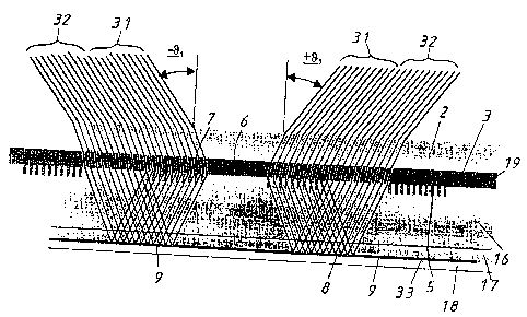
Two mutually parallel beams of light 31, 32, are shown, one of which passes
through
the free region 7 and the other through the lattice structure 5. Because of
the different diffraction of
the two light beams, the region 9 becomes visible from above through the
transparent region 6 as well
as through the lattice structure 7 at the viewing angle ~ 9~1.
Figures 4 and 5 show different methods for producing such a microstructure.
For producing the layers shown in Figure 4, as well as for producing
conventional
hologram sheets, it is necessary to prepare an embossing punch. This embossing
punch may be
produced, for example, by transferring a mask, prepared by electron beam
exposure, onto a nickel
_ _ ~ub~.ate. -This~riekef substrates ~ubs~querrtly used-as-~punel~fer-
embossing the sheet 19 ur-the _ _
embossing lacquer used in its place.
For producing the layer structure, shown in Figure 4a, initially the binary
lattice 5 is
embossed into the material 21 by means of the punch mentioned above. The
material 21 may consist
of a sheet but also of a lacquer, which can be cured, for example, by means of
ultra violet light.
Usually this material has a low refractive index n1 - 1.5. In a second step
(Figure 4 b), this embossing
is covered by a layer (material 22) with the refractive index n2, so that the
rifts of the lattice structure
5 are filled uniformly and a smooth surface results. Such a leveling is
possible by applying a lacquer
of low viscosity on the embossed microstructure 5.
It is necessary to fill the narrow, deep rifts completely with lacquer.
A further possibility of leveling consists of coating the embossed
microstructure 5
with a dielectric layer. Such a layer (material 25 of Figure 4 c) can be
produced by coating methods
such as vapor disposition or sputtering.
In both cases, a lacquer or a dielectric coating, it is necessary that the
refractive index
of the covering material is quite different from that of the material with the
embossed structure.
Usually, the refractive index for this material is higher than the refractive
index of the material 21, in
which the microstructure 5 was embossed.
{M:\4077\OM404VXY0597.DOC;1 }
CA 02417795 2003-O1-27
3356/0K043
PATENT
At the present time, by varying the lacquer, refractive indexes up to a
maximum of
n2=2.0 are available. Dielectric materials 25 with a higher refractive index
are also available. Zinc
sulfide and zirconium oxide, for example, would be typical materials.
In order to protect the layers constructed, the layer of "material 22" can be
provided
additionally with a layer of "material 23" (Figure 4 a). However, it is also
possible to do without this
layer in the event that the layer of "material 22" offers sufficient
protection against scratching (Figure
4 b).
However, a different variation of Figure 4 c is obtained if, instead of the
lacquer of
low viscosity, a lacquer (material 25) is used, which does not penetrate into
the narrow rifts of the
embossed microstructure 6. In this case, the air, which is in the rifts, is
enclosed and sealed by the
lacquer. Chambers 20 with the refractive index of n2=1.0, are formed in the
construction shown in
Figure 4 c.
It may, however, also be sufficient to provide the layer (material 22) with
the
embossed microstructure 5 with an adhesive system 24 in the manner shown in
Figure 4 d. The
adhesive system may, for example, be a thermoplastic hot-melt-type adhesive or
a heat-curing
adhesive. The microstructure S then does not need a further layer and is
applied directly on the card
body.
A further possible layer construction of the hologram-like sheet 19 is shown
in Figure
5. In order to prepare it, the microstructure (Figure 5 b) is transferred into
a sheet (Figure 5 a), which
is coated with a dielectric layer, with the help of an embossing punch.
Subsequently, the
microstructure is sealed with a lacquer. Usually, the dielectric layer
(material 22) has a refractive
index, which is higher than that of the material surrounding it. The
refractive index of the dielectric
layer may, for example, be n2. The surrounding material 21 or 22 usually has
the same refractive
index n,=nz=1.5.
In contrast to the sheets explained above, such a construction of layers has
the
advantage that the starting sheet can be produced more easily. In general, it
is difficult to coat a
microstructure 5, which is not flat and it is difficult to apply a homogeneous
leveling material. On the
other hand, it is state of the art to provide smooth sheets with a uniform,
dielectric layer.
Figures 8 and 9 show further, possible, examples of a lattice structure 5. It
is shown
here that the profile of the cross-member elements 30 need not necessarily be
rectangular.
Admittedly, a rectangular shape is preferred because of the optimum
utilization of the Bragg effect.
This effect is most clearly pronounced in the case of a binary rectangular
profile.
However, the invention is not limited to this. Profile forms, which deviate
from the
rectangular, are therefore also used for the cross-member element 29 or 30. An
approximately
trapezoidal cross-member element 30 is shown in Figure 8 and a half round,
elliptical or oval, cross-
member element 29 is shown in Figure 9. It has also already been pointed out
that the lattice structure
{M:\4077\OM404UXY0597.DOC;1 }
CA 02417795 2003-O1-27
3356/0K043
PATENT
need not necessarily be at the underside of the layer 3. It may also be
disposed on the upper side of
the latter or on both sides.
A further possibility for realizing the inventive, hologram-like sheet 19 is
shown in
Figures 10 and 11. In these cases, the sheet 19 is defined by a volume
transmission hologram. The
methods employed here differ from those used for the preparation for the
hologram-like sheet 19 in
Figures 4 a - d) or 5 a - c. The novel sheet has the same optical properties
shown in Figures 1 and 3.
Volume transmission holograms result when two beams are caused to interfere in
a
light-sensitive layer. In the light-sensitive layer, the refractive index of
the material is altered in the
regions of constructive interference. The "holographic recording film" of
DuPont is such a so-called
protopolymer.
One possibility of realizing this is shown in Figure 10. In this case, the
necessary
interference patterns are produced by the diffraction of the plane,
monochromatic illumination wave at
a plasma mask.
A plasma mask changes the phase position of an illumination wave. This is
achieved
by the difference in optical paths, which the illumination wave experiences
through such a mask. The
optical path through the region of the phase mask, shown in gray, is different
from that through the
surrounding region of the mask. The optical path is obtained by multiplying
the geometrical path
through the mask by the refractive index. Accordingly, the optical path
difference can be produced by
a modulation of the refractive index, by a change in the geometry or by a
combination of the two.
In the region of the phase lattice, the illumination wave is diffracted into
the 1 S' or -1 S'
order. Interference between the two wave fronts of the 1 S' and -1 S' order
comes about in the region of
a dichromate gelatin (preferably a photopolymer material). The refractive
index pattern, produced by
the interference of the wave fronts, is shown in the right part of the Figure.
In the region, in which
there is no phase mask, the illumination wave passes through the photopolymer
without forming an
interference pattern. In this way, a region 7 with a refractive index
modulation and a region 6 without
a refractive index modulation result in the photopolymer, as shown in the
right part of Figure 10.
Such a phase mask can be produced by etching a binary lattice in a glass
substrate.
The path or phase difference for the illumination wave is then produced by the
different optical path
length through the phase lattice.
A further procedure for realizing the volume transmission hologram is shown in
Figure 11. In this case, two illumination waves intersect at an angle on the
photopolymer.
It is a property of this material that its refractive index is changed under
the influence
of light. An illumination by an interference pattern images this after the
development as modulation
of the refractive index.
Accordingly, an interference pattern is formed there and a corresponding
refractive
index pattern also results there due to this illumination. The regions, which
are not to have a lattice
structure pursuant to the invention, are covered by an amplitude mask.
{M:\4077\OM404UXY0597.DOC;1 }
CA 02417795 2003-O1-27
3356/0K043
PATENT
An amplitude mask permits the photopolymer to be illuminated only in the
transparent regions (shown in gray in the drawing). In the other regions, the
mask is opaque (shown
in black in the drawing). Accordingly, regions with and without a refractive
index modulation arise in
the right part of Figure 11.
The only difference between a phase mask and an amplitude mask is the way in
which it is made. In both cases, the result is almost identical. For the phase
mask, only a coherent,
illumination wave is required in order to produce the interference pattern.
For the amplitude mask,
two coherent illumination waves are required. However, it is more complicated
to produce a phase
mask than an amplitude mask.
Amplitude masks are produced photolithographically or by electron beam
illumination. Phase masks can be produced, for example, by etching a binary
lattice. The amplitude
mask transmits the illumination waves only in the transparent regions. The
phase mask diffracts the
light in the region of the binary lattice. The diffracted light, so produced,
interferes. The transparent
and opaque regions of the amplitude lattice and also the regions of the phase
mask with and without a
phase lattice correspond to the regions 6 and 7 of Figures 1 and 3.
In both cases, the volume transmission hologram, so prepared, can also be used
as
sheet 19, which is claimed pursuant to the invention. The volume transmission
hologram is applied
on the information Garner by means of an adhesive system before or after the
personalization.
The same size data, given in Table 1, also applies to the order of magnitude
of the
binary lattice of the phase and amplitude mask.
A support sheet is no longer provided in Figures 10 and 11. Instead, the
photopolymer is shown with an adhesive system, which is required in order to
apply the sheet to the
card body. After the application, the mode of action of the sheet is precisely
as shown in Figures 1
and 3.
Figure 12 shows a plan view of representation of the binary information and
the
reading of the latter. Figure 12 a shows a defined plan view at an indefinite
viewing angle, at which
the two sets of information are mixed with one another. On the other hand,
Figure 12 b shows the
representation of one set of information at a defined viewing angle, while
Figure 12 c shows the other
set of information at a second viewing angle, which deviates from the first.
It is, moreover, shown in the general part of the specifications that a total
of three or
more sets of information can also be disposed on the information layer 33. In
this case, the third set
of information would be read separately from the two other sets of information
of Figures 12 b and c
at a defined, third viewing angle.
{M:\4077\OM404VXY0597.DOC;1 }
9
CA 02417795 2003-O1-27
3356/0K043
PATENT
List of Reference Numbers
card construction
layer
layer
layer
lattice structure
region (without lattice structure)
region (with lattice structure)
region (gray)
region (black)
distance (D) thickness
width (p)
width of cross-member (S)
distance of cross-member (G)
lattice period (/~)
lattice depth (d)
sheet
sheet
sheet
microstructured sheet
material
material
material
material
adhesive system
material
chamber
cross section of element
interstice
cross sectional element
cross sectional element
beam of light
beam of light
information layer
illumination wave
{M:\4077\OM404UXY0597.DOC;1 }
CA 02417795 2003-O1-27
3356/0K043
PATENT
phase mask
dichromate gelatin
support substance
lattice structure
lattice structure
wave front
wave front
amplitude mask
illumination wave
illumination wave
{M:\4077\OM404UXY0597.DOC;1 }
11