Note: Descriptions are shown in the official language in which they were submitted.
CA 02418575 2003-02-05
LIGI4T CONTROL DEVICE
BACKGROUND OF TI-IE II~TVENTION
The present invention relates to a light control device configured to
switch an optical path or limit it (i.e., to control the quantity of light) by
displacement of a moving plate and consequently a mirror or light shielding
plate mounted thereon.
Fig. 1A shows the construction of an optical switch which is an
example of a conventional light control device of this kind. The illustrated
optical switch is a 2-by-2 optical switch for switching optical paths of two
incoming rays B1 and B2 parallel to each other but opposite in direction.
On a moving plate 11 there are mounted four mirrors 12 as light
control means. The mirrors 12 are disposed at an angle of 45 degrees with
respect to the incoming rays B1 and B2, respectively, as depicted in Fig. 1A.
1 S The moving plate 11 is supported by two support beams 13 in a
manner to be displaceable in a direction vertical to the surface of the moving
plate 11 itself. The support beams 13 are projected from a pair of opposed
sides of the moving plate 11 of a square plate configuration, and are
respectively extended around it along its three sides. The extended ends of
the support beams 13 are fixedly coupled to stationary parts 15 on a frame
14 surrounding the moving plate 11.
Under the moving plate 11 is located a fixed electrode 16 at a
predetermined spacing as shown in Fig. 1B, and a base 17 with which the
fixed electrode 16 is formed integrally has its marginal portion joined to the
frame 14. The moving plate 11 opposed to the fixed electrode 16 functions
as a moving electrode.
In the optical switch of the above configuration, upon voltage
1
CA 02418575 2003-02-05
application across the moving plate 1 l and the fixed electrode 16, the
moving plate 11 is attracted down by electrostatic power toward the fixed
electrode 16, and upon removing the voltage, the moving plate returns to its
initial position.
Accordingly, the optical switch is able to switch the optical paths by
the mirrors 12 which undergo displacement as the moving plate 11 moves up
and down. That is, when the moving plate 11 lies at the position indicated
in Fig. 1B, the incoming rays Bl and B2 are reflected by the mirrors 12 to
travel as indicated by the solid lines marked with the arrows, whereas when
the moving plate 11 is at its lowered position, the mirrors 12 go out of the
optical paths, allowing the incoming rays B 1 and B2 to traveling in straight
lines without being reflected by the mirrors 12.
Figs. 2 and 3 show a sequence of steps involved in the manufacture
of the above optical switch. The optical switch is manufactured using two
base plates or substrates. Steps S 1 to S4 in Fig. 2 show steps of processing
the upper substrate, and steps S5 to S7 in Fig. 3 show steps of processing the
lower substrate.
The upper substrate is, in this example, a mufti-layered SOI (Silicon
On Insulator) substrate 24 with a Si02 layer 21 sandwiched between silicon
(Si) layers 22 and 23 as depicted in Fig. 2. The manufacturing process will
be described below step by step.
Step S 1: The SOI substrate 24 are coated all over its top and bottom
surfaces with thermally oxidized films 25 and 26, respectively.
Step S2: Patterns for the moving plate, the support beams and the
stationary parts are formed by photolithography over the thermally oxidized
film 25 on part of the top surface, then the thermally oxidized film 25 is
selectively etched away as patterned, arid the Si layer 22 is selectively
2
CA 02418575 2003-02-05
etched away using the thermally oxidized film pattern as a mask. On the
other hand, a frame pattern is formed by photolithography over the
thermally oxidized layer 26, and the thermally oxidized film 26 is
selectively etched away as patterned.
Step S3: The thermally oxidized film 25 remaining on the part of the
top surface is etched away, and a thick resist film is coated over the entire
area of the top surface and patterned to form mirror bodies, which are coated
all over its surface area with an Au film to form the mirrors 12.
Step S4: The Si layer 23 on the side of the bottom surface is
selectively etched away, and the Si02 layer 21 is selectively etched away to
form the frame 14. As a result, two stationary parts 15 are positioned on
the Si02 layer of the frame 14 composed of the S~i layer 2 and the Si02 layer
21, and the moving plate 11 carrying the mi~°rors 12 is supported by
the
stationary parts 15 through the support beams 13.
On the other hand, an Si substrate 27 is used as the lower substrate.
Referring to Fig. 3, the manufacturing process will be described below step
by step.
Step S5: The Si substrate 27 is coated all over its top and bottom
surfaces with thermally oxidized films 28 and 29, respectively.
Step S6: A fixed electrode pattern is formed by photolithography
over the thermally oxidized film 28, and the thermally oxidized film 28 is
selectively etched away as patterned.
Step S7: The substrate 27 is etched away as predetermined using the
pattern of the thermally oxidized film 26 as a mask, after which the
thermally oxidized film 28 are etched away. As a result, the upwardly
protruded fixed electrode 16 is formed on the base 17.
The Si substrate 27 and the SOI substrate 24 thus obtained are
3
CA 02418575 2003-02-05
integrated into a single-piece structure with the frame 14 fixedly mounted on
the base 17 by bonding, for instance. In this way, the optical switch shown
in Figs. 1A and 1B is manufactured.
In such a conventional a light control device as the above-described
optical switch of the construction in which the moving plate is used as a
moving electrode and displaced by electrostatic driving to switch or limit
optical paths by displacement of the mirrors or light shielding plates
mounted on the moving plate, the moving plate is drive in its widthwise
direction, that is, in the direction vertical to the plate surface.
Accordingly, the fixed electrode for electrostatic driving of the
moving plate needs to be disposed opposite the moving plate surface, but it
is difficult to obtain from one substrate the moving plate (the moving
electrode) and the fixed electrode bearing such a positional relationship to
each other. On this account, it is conventional to produce them separately
using two substrates and integrate them as by bonding.
Hence, the prior art manufacturing method involves patterning by
photolithography and etching for each of the two substrate and necessitates
their integration (by bonding) into a unitary structure; hence, these works
inevitably increase the number of man-hours, making the manufacture of the
light control device complicated and time-consuming.
SLT1VIMARY OF THE IN~1ENTION
It is therefore an object of the present invention to provide a light
control device that can be manufactured with a smaller number of
man-hours and with high accuracy.
The light control device according to the present invention
comprises:
4
CA 02418575 2003-02-05
side beams;
a moving plate having opposed side surfaces;
at least one pair of support beans extended in opposite directions
from said opposed side surfaces of said moving plate in parallel relation to
said moving plate and having its tip ends fixed to said side beams,
respectively, to support said moving plate in a manner to be elastically
displaceable in a plane in which the plate surface of said moving plate lies;
drive means for driving said moving plate relative to said side beams
in said plane in which said plate surface lies; and
light control means mounted on said moving plate, for controlling
incident optical beams in accordance with the displacement of said moving
plate by said drive means;
wherein said moving plate, said support beams, said side beams and
said drive means are formed by etching one substrate.
Said drive means may be formed moving planar electrodes extended
from sad side surfaces of said moving plate and a fixed planar electrode
disposed opposite said moving tomblike electrodes in common to them.
Alternatively, said drive means may be formed by moving tomblike
electrodes extended from sad side surfaces of said moving plate and a fixed
tomblike electrode disposed opposite said moving tomblike electrodes in
common to them.
The above light control device may have a construction in whicha
said paired support beams are extended from said side surfaces of said
moving plate at a predetermined angle of inclination thereto and
symmetrically arranged in respect to the center line parallel to the said
direction of displacement of said moving plate; said drive means is disposed
on either side of said moving plate in direction of displacement of said
5
CA 02418575 2003-02-05
moving plate; and said paired support beams are driven by said drive means
into snap action.
The above light control device may have a construction in which:
said paired support beams are extended from said side surfaces of said
moving plate at a predetermined angle of inclination thereto and
symmetrically arranged in respect to the center line parallel to the direction
of displacement of said moving plate; said drive means comprises plural sets
of a thermally expansive member and an energy-conversion mechanism for
converting thermal expansion of said thermal expansive member into a
pressure in said direction of displacement of said moving plate, said drive
means being capable of applying forward and backward pressures to said
moving plate; and, on said moving member being pressed by said
energy-conversion mechanism, said support beams performs snap action to
drive and displace said moving plate.
The above light control device may have a construction in which:
said light control means may be formed by mirrors to change optical paths
of said incident optical beams; or said light control means may be formed by
light shielding plates whose transmittance varies in the direction of
displacement of said moving plate to control the amounts of incident optical
beams transmitted.
Furthermore, in the above light control device said drive means may
be formed by moving planar electrodes extended from said opposed side
surfaces of said moving plate and a fixed planar electrode disposed opposite
said moving planar electrode, or by moving tomblike electrodes extended
from said side surfaces of said moving plate and a fixed tomblike electrode
disposed opposite said moving tomblike electrodes.
In the above optical control device, said substrate may be one of
6
CA 02418575 2003-02-05
silicon layers of a mufti-layered SiO2 substrate deposited all over its both
sides with silicon layers, and grooves for fixedly receiving optical fibers
may be cut in the other of said silicon layers.
BRIEF DESCRIPTION OF THE DRAWINGS
Fig. lA is a plan view showing the construction of a conventional
optical switch;
Fig. 1B is a sectional view taken along the line 1B-1B in Fig. lA;
Fig. 2 is a diagram showing a sequence of steps involved in the f rst
half of the manufacturing process of the optical switch depicted in Figs. 1 A
and 1 B;
Fig. 3 is a diagram showing a sequence of steps involved in the
second half of the manufacturing process of the optical switch;
Fig. 4 is an exploded perspective view illustrating an embodiment of
the present invention;
Fig. 5 is a plan view showing the construction of the part formed by
the lower Si layer in Fig. 4;
Fig. 6A is a diagram depicting an optical path switching operation of
the optical switch shown in Fig. 4;
Fig. 6B is a diagram depicting another optical path switching
operation of the optical switch shown in Fig. 4;
Fig. 7 is a diagram illustrating a sequence of steps involved in the
manufacture of the optical switch shown in Fig. ~;
Fig. 8 is a diagram for explaining another embodiment of the present
invention;
Fig. 9 is a perspective view, partly separated, of another embodiment
of the present invention;
7
CA 02418575 2003-02-05
Fig. 10 is a plan view showing the construction of the part formed by
the lower Si layer in Fig. 9;
Fig. 11 A is a graph showing the relationship between the
displacement of the support beam and the energy gathered therein in the
case of Fig. 5 embodiment;
Fig. 11B is a graph showing the relationship between the
displacement of the support beam and the energy gathered therein in the
case of Fig. 9 embodiment;
Fig. 12A is a diagram showing the one optical path switching
operation of the optical switch depicted in Fig. 9.;
Fig. 12B is a diagram showing the other optical path switching
operation;
Fig. 13 is a perspective view, partly taken. away; of another
embodiment of the present invention;
Fig. 14 is a plan view of the Fig. 13 embodiment;
Fig. 1 SA is a partial plan view for explaining the state in which the
moving part of the Fig. 13 optical switch is displaced in one direction by
electrostatic driving; and
Fig. 1 SB is a partial plan view for explaining the state in which the
moving part of the Fig. 13 optical switch is displaced in the other direction
by electrostatic driving.
DETAILED DESCRIPTION OF THE PREFERRED EMBODIMENTS
A description will be given, with reference to the accompanying
drawings, of embodiments of the present invention.
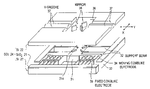
Fig. 4 is a diagrammatic showing of an optical switch structure as an
embodiment of the light control device of the present invention. In this
8
CA 02418575 2003-02-05
embodiment, the optical switch is a 2-by-2 optical switch as is the case with
the conventional optical switch depicted in Figs. 1A and 1B, and the switch
is formed by a mufti-layered S~I substrate 24 with an Si02 layer
sandwiched between Si layers 22 and 23. Incidentally, in Fig. 4 the part
formed by the upper Si layer 22 is shown separately of the Si~2 layer 21.
Fig. 5 is a top plan view of the structure of the portion formed by the
lower Si layer 23, which will be described first.
A moving plate 31 has a square plate-like structure, and narrow
support beams 32 are extended in pairs in opposite directions from the
opposite sides 31 a and 31 b of the moving plate 31 in alignment with each
other. The support beams 32 are extended in parallel to the top surface 31 c
of the moving plate 31 and at right angles to the side surfaces 31 a and 31 b
thereof. In this example two support beams 32 are extended from either
one of the side surfaces 31 a and 31 b; that is, two pairs of support beams 32
are used.
The support beams 32 have their extended ends fixedly coupled to
side beams 33 disposed at right- and left-hand sides, and consequently, the
moving plate 31 is supported at its both ends by the side beams 33 through
the two pairs of support beams 32 in a manner to be displaceable in the
X-direction. In the following description, as indicated in Fig. 5, the
direction parallel to the top surface 31 and side surfaces 31 a and 31 b of
the
moving plate 31 will be called the X-direction and the direction
perpendicular to the side surfaces 31 a and 31 b will be Galled the Y
direction.
Moving comblike electrodes 34 are extended in the ~'-direction from
the both side surfaces 31a and 31b of the moving plate 3lnear its one end in
the X-direction. The tomblike electrodes 34 are each composed of a base
portion extended in the 1'-direction and comb teel:h 34b projecting in the
9
CA 02418575 2003-02-05
X-direction from the base portion 34a at regular intervals in the Y direction.
A fixed tomblike electrode 35 disposed opposite the both moving
tomblike electrodes 34 is composed of a base portion 35a extended in the
Y direction and comb teeth 35b projecting in the X-direction from the base
portion 35a at regular intervals in the Y direction. The moving tomblike
electrode 34 and the fixed tomblike electrode 35 are arranged with their
comb teeth 34b and 35b in meshing engagement just like an interdigital
electrode. In this example the movable and fixed tomblike electrodes 34
and 35 constitute drive means for displacement of the moving plate 31 in the
X-direction by electrostatic driving.
On the other hand, the upper Si layer 22 has, as shown in Fig. 4, a
centrally located opening 36 and two pairs of V grooves 37 extended in the
Y direction from opposite sides of the opening 36 for fixedly receiving
optical fibers. In the ~1 grooves 37, though not shown in Fig. 4, optical
fibers each carrying a lens at one end thereof, for instance, are fixedly
mounted in alignment with each other.
Four mirrors 38, located in the opening 3C to serve as light control
means, have their bodies formed by the Si layer 2.2 and mounted through a
Si02 layer 21 on the moving plate 31 formed by the Si layer 23. The
mirrors 38 are each arranged at an angle of 45 degrees with respect to
incident light.
Figs. 6A and 6B show how to switch optical paths in the optical
switch of the above-described construction. By application a voltage
across the moving and fixed tomblike electrodes 34 and 35 in the state of
Fig. 6A, the moving tomblike electrode 34 is attracted by electrostatic force
to the fixed tomblike electrode 35, flexing the support beams 32 and hence
displacing the moving plate 31 in the X-direction and switching the optical
CA 02418575 2003-02-05
paths as depicted in Fig. 6B.
Next, a description will be given, with reference to Fig. 7, of a
sequence of steps S 1 to S9 involved in the manufacture of the optical switch
of this embodiment. Incidentally, the Si layer 23 sho~NS the section of each
of the comb teeth 34b and 35b, and the Si layer 22 shows the section of the
V groove 37.
Step S 1: The thermally oxidized films 25 and 26 are formed all over
the top and bottom surfaces of the S~I substrate 24, respectively.
Step S2: A through hole 41 is formed by photolithography and
etching through the bottom-side thermally oxidized film 26 at a
predetermined place.
Step S3: An Au/Cr two-layer film is formed over the entire area of
the bottom surface, and selectively etched away in the form of an electrode
pad. Though not shown in Figs. 4 and 5, the electrode pad 42 is provided
on each side beam 33 and the base portion 35a of the fixed comblike
electrode 35.
Step S4: Patterns for the moving plate, the support beams, the side
beams, the moving comblike electrode and the fixed comblike electrode are
formed by photolithography all over the thermally oxidized film 26, after
which the bottom-side thermally oxidized film 26 is selectively away as
patterned.
Step S5: Patterns for the optical fiber receiving ~V grooves, the
opening and mirrors are formed by photolithography all over the top-side
thermally oxidized film 25, after which the thermally oxidized film 25 is
selectively away as patterned.
Step S6: The bottom-side Si layer 23 is selectively removed by deep
dry etching, using the thermally oxidized film pattern 26 as a mask.
11
CA 02418575 2003-02-05
Step S7: The top-side Si layer 22 is selectively removed by KOH wet
etching, using the thermally oxidized film pattern 25 as a mask.
Step S8: The mirror bodies are coated all over their surfaces with an
Au film 43 to form the mirror 3 8.
Step S9: The remaining SiO2 layer is selectively removed by wet
etching except the Si02 layer 21 overlying the side beams 33 and the base
portion 35a of the fixed tomblike electrode 35, the Si02 layer 21 underlying
each mirror 38 and the thermally oxidized film 26 of each electrode pad
portion 42. In this way, the optical switch of Fig. 4 is obtained.
As described above, in this example, the moving plate 31 is driven in
parallel to its top surface 31 c to switch the optical paths, and the moving
plate 31 supported by the support beams 32 and the drive means composed
of the moving and fixed tomblike electrodes 34 and 35 for driving and
displacing the moving plate 31 are formed by a single
photolithography-etching process of one substrate.
Accordingly, the optical switch of this example can be manufactured
with a smaller number of man-hours than in the manufacture of the
conventional optical switch of the construction that uses two substrates and
drives the moving plate to displace in the direction vertical to the plate
surface.
Further, since the fixed and moving tomblike electrodes forming the
drive means for electrostatic driving the moving plate can be formed
simultaneously (by photolithography-etching), they can be formed with high
accuracy-this permits easy fabrication of high-precision tomblike
electrodes which mesh with each other as described above.
In this example the substrate for forming the moving plate and the
drive means is a silicon substrate, which is the one Si layer of the SOI
12
CA 02418575 2003-02-05
substrate, and the other Si layer is used for forming the V grooves and the
mirrors; accordingly, the moving plate, the V grooves and the mirrors, which
are arranged three-dimensionally can be miniaturized with ease.
Fig. 8 schematically illustrates a modified form of the above
embodiment, in which the moving and fixed comblike electrodes 34 and 35
are replaced with moving and fixed planar electrodes 51 and 52 which are
disposed opposite each other to form the means for driving the moving plate
31.
In this case, when the fan der VUaals force resulting from the contact
between the moving and fixed planar electrodes is larger than the elastic
restoring force of the support beams 32, the electrodes stick fast together (a
phenomenon that the moving electrode will not restore to its initial position
even if the applied voltage is removed). To avoid this, it is necessary to
perform non-contacting drive of the moving electrode by applying voltage
within a range that the moving electrode is not brought into contact with the
fixed electrode. In this instance, the moving and the fixed electrodes need
to be spaced apart more than 3D, i.e. more than three times the electrode
driving distance D necessary for switching the optical paths of optical beams,
in which case the voltage necessary for driving the moving electrode by the
distance D is as high as about 5.2 times the voltage needed for contacting
drive.
In contrast thereto, the comblike opposed electrode structure is very
advantageous in easy position control, non-contacting drive and low voltage
consumption.
While in the above the present invention has been described as being
applied to the optical switch of the type in which the mirrors mounted on the
moving plate are displaced by electrostatic drive of the moving plate to
13
CA 02418575 2003-02-05
switch the optical paths, the invention is not limited specifically to such an
optical switch and the displacement of the mirrors. For example, the
invention is applicable as well to a light control device like a so-called
variable optical attenuator (V~A) in which light shielding plates, whose
transmittance varies continuously or on a stepwise basis in the X-direction,
are mounted as light control means on a moving plate and the light shielding
plates are displaced in the X-direction to thereby control the optical paths
(to
control the amounts of light passing through the shielding plates).
Incidentally, since the above-described drive means using
electrostatic force holds the moving plate in its displaced position only
during the voltage application, continued application of voltage is needed to
hold optical paths with the moving plate displaced. This presents a
problem that the optical paths cannot be maintained upon occurrence of a
trouble on the part of the drive power supply, such as a power failure.
Fig. 9 and 10 illustrate a modified form of the Figs. 4-5 embodiment
which is equipped with a function of holding the moving plate in position
(hereinafter referred to as a latch function).
In this example, as depicted in Fig. 10, the two pairs of support
beams 32 are extended at a predetermined angle of inclination to the side
surfaces 31 a and 31 b of the moving plate 31 and the two pairs of support
beams 32 are symmetrically arranged in respect to the center line of the
moving plate 31 parallel to the X-direction.
That is, this embodiment has a bi-stable structure in which such
tilting of the support beams 32 provides a peak in the energy that are stored
in the support beams 32 in accordance with their displacement.
As shown in Fig. 11 A, in the case of the support beams disposed in
parallel to the Y direction, the energy that is stoned in each support beam
14
CA 02418575 2003-02-05
monotonously increases and decreases with an increase and a decrease in the
displacement in the X-direction. To maintain desired displacement of such
a support beam, it is necessary to keep on applying energy that balances
with the energy of the support beam at its current position.
In contrast thereto, in the case of the support beams inclined to the
Y direction, the energy that is stored in each support beam has a peak with
respect to an increase and a decrease in the displacement as shown in Fig.
118. In this case, once supplied from the outside with energy just a little
larger than the peak, the support beam stays at a certain position even if the
external energy application is stopped. That is, such an energy application
displaces the support beam to a predetermined position through snap action
and holds it there stably.
Incidentally, forward and backward forces (electrostatic attractive
forces) are required for the X-direction displacement of the moving plate 31
through the snap action of the support beams disposed at a predetermined
angle of inclination. To meet this requirement, in the Figs. 9-10
embodiment drive means composed of the moving and fixed comblike
electrodes 34 and 34 is disposed as well on the side of the moving plate 32
opposite the afore-described drive means in the X-direction.
Figs. 12A and 12B show how the moving plate 31 is driven for
displacement by the drive means disposed on either side of the moving plate
31 in the X-direction to switch optical paths.
Although the above has described the constructions in which the
drive means is formed by opposed electrodes and the moving plate is driven
by electrostatic force, the moving plate can be displaced as well through
utilization of other force than the electrostatic one as described below.
Figs. 13 and 14 illustrate an optical switch provided with drive
CA 02418575 2003-02-05
means which utilizes thermal expansion. In this example, as is the case
with the Figs. 9-10 embodiment, the support beams 32 are inclined in
respect of the Y direction and adapted for snap action. In Fig. 13 there is
not shown the part which is formed by the upper Si layer 22 of the SOI
S substrate in Fig. 9. And, Fig. 14 is a top plan view of the structure formed
by the lower Si layer 23 depicted in Fig. 13.
Referring to Fig. 14, the construction of the drive means will be
described below.
In this example the drive means for driving the moving plate 31
comprises four sets of thermally expansive members 61 and
energy-conversion mechanisms 62 for converting thermal expansion of the
thermally expansive members 61 into pressures in the X-direction. With
this configuration, forward and backward pressures by the two pairs of
opposed drive means can be applied in the X-direction to the pressing parts
71 projecting in the Y direction from the both side surfaces 31 a and 31 b of
the moving plate 31.
Each thermally expansive member 61 is extended in the Y direction
and fixedly connected at its base end to one fixed electrode 63.
The energy-conversion mechanisms 62 each comprise an L-shaped
arm carrying at its tip a pressing projection 64 and very narrow coupling
portions 66 and 67 protrusively provided on both sides of the base end
portion of the arm 65 at positions slightly displaced in the X-direction. The
one coupling portion 66 is connected to the tip of the thermally expansive
member 61, whereas the other coupling portion 67 is fixed to a fixed
electrode 68. Incidentally, the portion P of the arm 65 on which the
coupling portion 67 is protrusively provided serves as a point of force and
the portion Q on which the coupling portion 67 is protrusively provided
16
CA 02418575 2003-02-05
functions as a fulcrum.
With the drive means of the above construction, upon voltage
application across the fixed electrodes 63 and 68 to feed current to the
thermally expansive member 61, the resulting Joule's heat expands the
thermally expansive member 61.
The point of force P is pressed by the thermal expansion of the
member 61, and consequently, the arm 65 turns about the fulcrum Q, and the
projection 64 is displaced substantially in the X-direction, pushing the
pressing part 71 projecting from the moving plate 31.
As a result, the support beam 32 performs snap action to shift from
the state shown in Fig. I SA to the state in fig. 15~, by which the moving
plate 13 is displaced.
In the case of displacing the moving plate 31 in the direction
opposite to the above, voltage is applied across the fixed electrodes 63and
68 on the side for pressing the moving plate 31 in the opposite direction.
Letting b represent the distance between the fulcrum Q and the point
of force P and L represent the length of the side of the L-shaped arm 65 on
which the projection 64 is protrusively provided, the displacement of the
projection 64 is a large value corresponding to L!b for the amount of thermal
expansion a of the thermally expansive member 61.
In this example, the support beams 32 are each fixed to the side
beam 33 through a damper 72-this allows more ease in the snap action of
the support beam 32.
EFFECT OF THE INVENTION
As described above, according to the present invention, the moving
plate is displaced in parallel to the plate surface, and the drive means for
the
17
CA 02418575 2003-02-05
displacement of the moving plate is formed of thE: same substrate as the
moving plate; hence, they can be formed simultaneously by a single
photolithography-etching process.
Accordingly, the present invention makes it possible to manufacture,
with a small number of man-hours but with high accuracy, a light control
device, such as an optical switch or variable optical attenuator, in which the
moving plate is displaced to perform switching of optical paths or control
the amount of light by displacement of the mirrors or light shielding plates
mounted on the moving plate.
Furthermore, when the drive means is formed by moving and fixed
comblike electrodes, their position control is easy, their sticking by direct
contact can be avoided, and the drive voltage can be reduced.
Moreover, by forming the support beams a little aslant with respect
to the side surfaces of the moving plate, it is possible to obtain a device in
which the support beams perform snap action to provide the latch function.
Once displaced, the moving plate needs no power supply to stay at the
displaced position-this provides increased reliability for abnormality of the
drive power supply, for instance.
25
18