Note: Descriptions are shown in the official language in which they were submitted.
CA 02418703 2003-02-04
1
DESCRIPTION
METHOD FOR PRODUCING SILICON
Technical Field
The present invention relates to a method for producing
silicon applicable to a semiconductor or photovoltaic power
generation from a silane. More specifically, the present
invention relates to a production method of high purity
silicon which comprises removing and recovering silicon
deposited on a substrate in a silicon deposition reactor from
the substrate without cooling the silicon and with small
effort so as to improve a rate of operation of the reactor.
Background Art
A variety of methods for producing silicon to be used
as a raw material for a semiconductor or photovoltaic system
have heretofore been known, and some of them are already
actually used in industry.
One of the actually used methods is a method called
as a Siemens method. This method is a method in which a thin
silicon filament which serves as a substrate for deposition
is disposed in a bell jar and then heated by energization
and trichiorosilane (SiHC13) or monosilane (SiH4) is then
brought into contact with the substrate so as to cause silicon
to be deposited in solid form. The method is the most
generally practiced method at present.
In the Siemens method, after termination of the
energization, the bell jar is opened after the silicon
filament which is a deposit is allowed to fully cool down,
and after the fragile deposit is carefully recovered, another
thin silicon filament must be disposed with high accuracy.
Therefore, considerable effort is required each time the
deposit is recovered, and a time interval between depositions
CA 02418703 2003-02-04
2
is long, so that a rate of operation of the deposition reactor
is low.
Meanwhile, methods for continuously recovering
silicon deposited in a deposition reactor are proposed in
JP-A 59-121109, JP-A 51-37819 and JP-A 2002-29726. These
are methods in which while silicon is being deposited in a
molten state on a surface of a substrate heated at least to
the melting point of silicon by bringing a silane into contact
with the surface of the substrate, the molten deposit is
recovered from the surface of the substrate as it is and then
extracted from the reactor as molten silicon or
cooled/solidified silicon.
Since these methods carry out deposition of silicon
at high temperatures, these methods exhibit very good
deposition efficiency and can produce silicon at a low cost.
However, molten silicon obtained by these methods has such
strong reactivity that it is even called "super solvent"
(universal solvent) and has a problem that it is liable to
be contaminated by the surface of the substrate with which
the molten silicon makes contact. Accordingly, it has been
difficult in some cases to obtain high purity silicon which
can be used particularly in semiconductors.
An object of the Invention
Therefore, an object of the present invention is to
provide a silicon production method which can deposit and
recover silicon usable in a semiconductor or photovoltaic
power generation from a silane continuously, can improve a
rate of operation of a reactor thereby, and can produce high
purity silicon continuously as compared with a conventional
silicon production method which causes silicon to be
deposited in a molten state.
Other objects and advantages of the present invention
will be apparent from the following description.
CA 02418703 2003-02-04
3
Disclosure of the Invention
According to the present invention, the above object
and advantage of the present invention can be achieved by
repeating, in the same apparatus, a step of depositing
silicon as a solid by heating a surface of a substrate to
a temperature lower than the melting point of the silicon
and a step of causing a portion or all of the deposited silicon
to melt and drop by heating the surface of the substrate to
a temperature equal to or higher than the melting point of
the silicon when the deposition of the silicon in solid form
has proceeded to a certain point.
That is, according to the present invention, there is
provided a method for producing silicon which comprises a
- 15 step (hereinafter referred to as "step 1") of depositing
silicon on said surface by bringing a silane into contact
with the surface of a substrate while the surface of the
substrate is heated to and kept at a temperature lower than
the melting point of the silicon and a step (hereinafter
referred to as "step 2" ) of melting a portion or all of the
deposited silicon and to drop and recover the melted silicon
from the surface of the substrate by raising the temperature
of the surface of the substrate.
In the above method of the present invention, by
depositing silicon in solid form, the silicon is hardly
contaminated by the substrate at the time of deposition of
the silicon. Further, for recovery of the silicon, by
causing at least silicon deposited on the surface of the
substrate to melt and drop from the substrate, time during
which the molten silicon is in contact with the surface of
the substrate can be shortened as compared with a
conventional method in which silicon remains in a molten
state after deposited. As a result, contamination caused
by contact between the substrate and the molten silicon can
CA 02418703 2003-02-04
4
be reduced effectively. Further, according to the method
of the present invention, deposition and recovery of silicon
can be carried out continuously. In addition, since speed
at which silicon is deposited on the surface of the substrate
reaches a maximum in a temperature range slightly lower than
the melting point of the silicon, a temperature range in which
the deposition speed is high can be selected as compared with
the conventional melt-deposition method, whereby
productivity can be improved.
Brief Description of the Drawings
Fig. 1 is a conceptual diagram showing the steps in
the method of the present invention using a reactor of a
representative embodiment.
Fig. 2 is a conceptual diagram showing the steps in
the method of the present invention using a reactor of another
representative embodiment.
Fig. 3 is a schematic diagram showing another
embodiment of the reactor used in the present invention.
Fig. 4 is a schematic diagram showing another
embodiment of the reactor used in the present invention.
Best Mode for Carrying out the Invention
The step (1) of the present invention is a step of
depositing silicon by bringing a silane into contact with
the surface of a substrate while the surface of the substrate
is heated to and kept at a temperature lower than the melting
point of the silicon.
An example of the silane used in the above step (1)
is a compound represented by the following formula:
SiaHbXc
(wherein X is a halogen atom, alkoxyl group or alkyl group,
a is a positive integer, and b and c are each independently
0 or a positive integer, provided that a, b and c satisfy
CA 02418703 2003-02-04
a relationship of 2a + 2 = b + c).
The halogen atom represented by X is preferably
chlorine. The alkoxyl group is preferably an alkoxyl group
having 1 or 2 carbon atoms, and the alkyl group is preferably
5 an alkyl group having 1 or 2 carbon atoms.
Specific examples of the silane include silane
hydrides such as monosilane (SiH4), disilane (S12H6) and
trisilane (Si3H8); halosilanes such as monochlorosilane
( SiH3Cl ) , dichlorosilane ( SiH2C12 ) , trichiorosilane ( SiHC13 )
and silicon tetrachloride (SiC14); alkoxysilanes such as
triethoxysilane (SiH(C2H5O)3) and tetraethoxysilane
( Si ( C2H50 ) 4); alkylsilanes such as methylsilane ( SiH3CH3 ) and
dimethylsilane (SiH2(CH3)2); and alkylhalosilanes such as
methyldichlorosilane (SiHC12CH3), methyltrichlorosilane
(SiC13CH3), dimethylchlorosilane (SiHCl(CH3)2) and
dimethyldichlorosilane ( SiC12 ( CH3 ) 2 ) .
When silicon obtained by the method of the present
invention is used as a raw material for a semiconductor or
photovoltaic power generation, the silane hydride,
halosilane and alkoxysilane among the above silanes are
preferably used as main components. Of these, monosilane,
disilane, dichiorosilane, trichlorosilane, silicon
tetrachioride, triethoxysilane and tetraethoxysilane all of
which can be purified to high purity are more preferable,
and monosilane, dichiorosilane, trichlorosilane and silicon
tetrachloride all of which can be industrially mass-produced
and are widely used are particularly preferably used. These
silanes can be used alone or in combination of two or more.
It is advantageous that these silanes are fed into a
reaction system in gaseous form either solely or together
with hydrogen as required.
In the present invention, it is easy and preferable
to heat the substrate by a method using an electric current
or electromagnetic wave.
CA 02418703 2003-02-04
6
For example, when the substrate is heated by means of
an electromagnetic wave, an electromagnetic wave having a
frequency of several hundreds of Hz to several tens of GH2
can be used. In this case, appropriate frequency is selected
as required according to the material and shape of the
substrate to be heated.
In the present invention, the substrate for depositing
silicon on its surface must be composed of a material which
can be heated directly or indirectly to a temperature higher
than or equal to the melting point of the silicon.
Illustrative examples of the material include a carbon
material typified by graphite and a ceramic material such
as silicon carbide. The carbon material is the most
preferable.
When the above carbon material is used as the substrate,
a portion or all of the material is converted into silicon
carbide by making contact with molten silicon. In the
present invention, the material in that state can be used
as the substrate.
Further, the surface portion of the above substrate
which makes direct contact with silicon to be deposited may
be composed of a material which is relatively resistant to
molten silicon. To be more specific, when the substrate is
heated by means of an electromagnetic wave, the surface
portion is preferably coated with a material such as silicon
nitride, silicon carbide or pyrocarbon. A method for
carrying out the coating is not limited. It is convenient
to carry out the coating by means of a separately molded
insert.
One of important objects of the present invention is
to prevent deterioration of the substrate by molten silicon
and contamination of silicon products caused by the
deterioration of the substrate, with respect to the
conventional method for depositing silicon at the melting
CA 02418703 2003-02-04
7
temperature of the silicon. Therefore, in the step (1) where
silicon is deposited by contact between a raw material gas
and the substrate, it is important to keep the temperature
of the surface of the substrate at a temperature lower than
the melting point of the silicon.
More specifically, in the conventional method for
depositing silicon in a molten state, since deposited, molten
silicon is always in contact with the substrate, the
deposited silicon is constantly subjected to a chance of
contamination. Meanwhile, in the step (1) in the present
invention, since silicon is deposited in solid form, most
of deposits are successively deposited on the surface of high
purity solid silicon regardless of the material of the
substrate, and the deposit has essentially high purity as
in the case of the Siemens method. Further, by rendering
the temperature of the deposition as close to the melting
point of silicon as possible, the deposition can be further
accelerated.
Further, in the step (1) of the present invention, since
the size of the deposition substrate is not limited by the
surface tension and tare weight of molten silicon, it can
be rendered sufficiently large, whereby an industrial-scale
production amount can be secured.
The temperature of the surface of the substrate in the
step (1) is preferably at least 600 C at which silicon is
deposited. However, in order to improve efficiency of
deposition of silicon, it is preferably at least 1,100 C,
more preferably higher than 1, 250 C, most preferably at least
1, 350 C.
These preferable deposition temperatures are
conditions which are not used easily in the conventional
Siemens method and are temperatures which can be used only
in the method of the present invention. That is, in the case
of the Siemens method, when the above deposition temperature
CA 02418703 2003-02-04
8
is 1,100 C, the surface of an accumulated deposit becomes
quite uneven, so that normal deposition becomes difficult
to continue, while when the above deposition temperature is
1, 250 C or higher, there arises a very high possibility in
Siemens method that a deposit may be fused.
Further, an upper limit of the deposition temperature
of silicon in the step (1) is lower than the melting point
of the silicon. Although there are a variety of different
opinions on the melting point of silicon which is the upper
limit temperature, it should be understood that the melting
point is within a range of 1,410 to 1,430 C.
In the step (2) of the present invention, the
temperature of the surface of the substrate is increased to
a temperature equal to or higher than the melting point of
silicon, and a portion or all of deposited silicon is caused
to melt and drop from the surface of the substrate so as to
be recovered.
Further, in the step (2), it is sufficient to increase
the temperature of the surface of the substrate to at least
a temperature at which the deposited silicon melts, i.e.,
the melting point of the silicon. However, as the surface
temperature becomes higher, more energy than necessary is
consumed, and in some cases, deterioration of the material
of the substrate is accelerated. Accordingly, the surface
temperature is more preferably not higher than 1,600 C.
In the step (2) of the present invention, a portion
or all of silicon deposited on the surface of the substrate
is caused to melt and drop. Thus, when time during which
the temperature of the substrate is raised to and kept at
a temperature equal to or higher than the melting temperature
of silicon is defined as recovery time, the recovery time
is desirably as short as possible so as to prevent
contamination of recovered silicon and deterioration of the
material of the substrate and to improve a rate of operation
CA 02418703 2003-02-04
9
of the deposition reactor. That is, the recovery time is
preferably less than 30%, more preferably less than 10%, most
preferably less than 5% of total operation time.
In the above step (2), to cause a portion or all of
silicon deposited on the surface of the substrate to melt
and drop, the surface of the substrate having the silicon
thereon is heated to a temperature equal to or higher than
the melting point of the silicon as described above. As means
for increasing the temperature of the surface of the
substrate, a method of increasing the output of the foregoing
electric current or electromagnetic wave for heating is
generally used. Further, a method of reducing the amount
of gas flowing in the reactor may also be used alone or in
combination with the above method.
In this case, in order to cause the silicon deposited
on the surface of the substrate to drop stably, as for heating
of the surface of the substrate in reactor, it is preferably
to enable it to control independently the temperature of each
portion of the substrate surface. More specifically, in an
embodiment in which the substrate is heated by means of an
electromagnetic wave, it is recommended to use a reactor in
which induction heating coil for applying the
electromagnetic wave is divided into a plurality of layers
and the output of each of the divided layers can be controlled
independently.
In the present invention, a method of increasing the
temperature of the surface of the substrate at least to the
melting point of silicon may be, for example, a method of
increasing the output of induction heating coil, in a case
where the substrate is heated by means of an electromagnetic
wave.
Although the embodiment in which the substrate is
heated by use of an electromagnetic wave has been mainly
described above, it is also possible to heat the substrate
CA 02418703 2003-02-04
by energizing the substrate.
Meanwhile, silicon is a semiconductor and exhibits
considerably high conductivity at high temperatures where
a deposition reaction takes place. Therefore, when a
5 conductive substrate is used and heated by passing a current
through the substrate so as to deposit silicon on the surface
of the substrate, the current inevitably passes through the
deposited silicon. As the current is increased so as to melt
the deposited silicon as described above, a portion of the
10 surface of the silicon which makes contact with the substrate
starts to melt, and a current density converges to the portion.
As a result, the contact surface melts preferentially from
the portion as a starting point, and the silicon deposited
on the surface of the substrate can be caused to drop.
Of the foregoing heating methods, the method of heating
the substrate by means of an electromagnetic wave is more
preferable as the heating method of the present invention
because melting of silicon by heating of the substrate is
not influenced by the thickness or crystal state of the
deposited layer.
In the method of the present invention, by adopting
the step (2) of melting and recovering a portion or all of
a deposit on the surface of the substrate, such operations
in a batch process required in the conventional Siemens
method as replacement of gas inside a bell jar, opening of
the bell jar and setting of a new silicon filament can be
all left out, thereby improving a rate of operation of a
reactor significantly.
Hereinafter, the present invention will be described
in more detail with reference to the attached drawings.
However, the present invention shall not be limited to
embodiments illustrated in these attached drawings.
Figs. 1 and 2 are conceptual diagrams illustrating the
steps in the method of the present invention using reactors
CA 02418703 2003-02-04
11
in which a substrate is heated by means of an electromagnetic
wave (high-frequency wave).
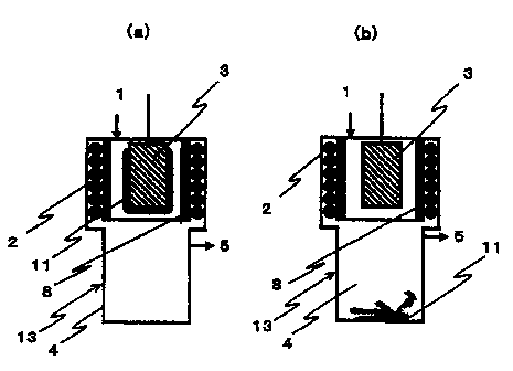
The reactors shown in Figs. 1 and 2 comprise a casing
13 having a feed port 1 for feeding a silane as a deposition
raw material, a heater 2 for generating an electromagnetic
wave, a substrate 3 which is heated by means of an
electromagnetic wave, a recovery part 4 for recovering a
dropped deposit, and an exhaust gas outlet 5. In this case,
between the heater 2 for generating an electromagnetic wave
and the substrate 3 to be heated, as shown in Figs. 1 and
2, a partition wall 8 which is made of a material which does
not block an electromagnetic wave is preferably placed so
as to isolate the heater 2 from an atmosphere in which the
substrate 3 exists.
As the material which does not block an electromagnetic
wave, a material having heat resistance and insulation
properties such as quartz, SIALON or aluminium nitride is
suitable.
Further, Fig. 1 shows an embodiment in which the
substrate 3 is in the form of a stick and silicon is deposited
on the external surface of the substrate, and Fig. 2 shows
an embodiment in which the substrate has a cylindrical shape
which opens downwardly and silicon is deposited on the
internal wall of the substrate. Of these embodiments,
particularly, the embodiment (Fig. 2) in which the substrate
has a cylindrical shape is suitable since heating efficiency
is good.
Further, in Figs. 1 and 2, (a) shows a state of silicon
11 being deposited on the surface of the substrate by the
step (1), and (b) shows a state of the silicon 11 caused to
melt and dropped by the step (2).
In the above step (1), a seal gas is preferably fed
so as to prevent the raw material gas from making contact
with the surface of the substrate other than a surface area
CA 02418703 2003-02-04
12
where the silicon is deposited.
Fig. 2 shows an embodiment in which a seal gas is fed
into space between the cylindrical substrate and the raw
material gas feed port 1 from a seal gas feed port 9. As
the seal gas, gas such as hydrogen or argon is suitably used.
Further, when a reaction reagent which produces the
raw material gas by reacting with silicon is fed continuously
or intermittently together with or in place of the above seal
gas, deposition of the silicon out of the deposition area
can also be prevented. As the reaction reagent, hydrogen
chloride or silicon tetrachloride is used, for example.
Further, when the above cylindrical substrate is used,
it is also possible that silicon tetrachloride and hydrogen
are fed into space surrounding the external surface of the
cylindrical substrate, i.e., space between the substrate 3
and the partition wall 8 as shown in Figs. 2 and 4, and
trichlorosilane is produced by use of heat generated in the
space. A portion of the produced trichlorosilane is used
in the deposition reaction of silicon on the internal surface
of the cylindrical substrate, and the remaining
trichlorosilane is recovered from the exhaust gas outlet 5
and can be recycled as a raw material gas after subjected
to known purification means.
Furthermore, in the embodiments in which the partition
wall 8 which is made of a material which does not block an
electromagnetic wave is inserted, the above seal gas is
preferably fed into between the casing 13 and the partition
wall.
Fig. 3 shows a conceptual diagram of a representative
reactor using current-based heating means in the present
invention. In this case, as in the case of the reactors shown
in Figs. 1 and 2, a raw material gas feed port 1, an exhaust
gas outlet 5 and a recovery part 4 are provided.
As shown in Fig. 3, a substrate 3 may be formed of
CA 02418703 2003-02-04
13
bar-shaped materials connected to each other so as to be
energized. Alternatively, it is also acceptable for another
embodiment that the substrate is composed of an insulating
material, a heating element which generates heat by
energization is prepared independently of the substrate, and
the substrate is heated by means of the heating element so
as to electrically isolate the heating element from silicon
to be deposited on the substrate. To be more specific about
the latter embodiment, the heating element which generates
heat by energization may be placed around the external
surface of the above cylindrical insulating substrate so as
to deposit silicon on the internal surface of the substrate,
or the above heating element may be placed inside of an
insulating substrate having space therein so as to deposit
silicon on the external surface of the insulating substrate.
In the above embodiments in which the substrate is
heated by means of the heating element which generates heat
by energization, switching between a temperature for causing
silicon to be deposited and a temperature for melting the
deposited silicon can be done by adjusting the amount of an
electric current. In this case, a current power supply 6
for properly adjusting the temperature of the substrate and
the temperature of a deposition surface is used in place of
the electromagnetic wave generator 2. As the above current
power supply 6, either of an AC power supply and a DC power
supply can be suitably used.
In the present invention, a method of taking the silicon
11 out of the recovery part 4 is not particularly limited.
Fig. 4 shows a conceptual diagram of a reactor having a
structure suitable for carrying out the method of the present
invention on an industrial scale. In Fig. 4, as an embodiment
for taking the silicon 11 out of the recovery part 4, a
structure in which space for the deposition reaction and the
recovery part can be separated from each other by means of
CA 02418703 2003-02-04
14
an atmosphere separator 7 is shown. More specifically, a
representative embodiment of the atmosphere separator is an
embodiment in which a saucer is slid so as to separate an
upper atmosphere from a lower atmosphere.
When the reactor used in the present invention has such
a structure with an atmosphere separator as described above,
dropped and recovered silicon can be taken out of the reactor
with the recovery part 4 in its lower portion opened while
the deposition reaction is continued in the silicon
depositing space in its upper portion.
As means for taking the silicon out of the reactor,
it is preferable to receive dropping silicon 11 in a saucer
placed in the recovery part 4 and take the silicon out
of the reactor when it is accumulated in a predetermined
15 amount.
Meanwhile, when the space for the deposition reaction
is not physically separated from the recovery part, dropped
and recovered silicon can be taken out of the reactor after
feeding of the deposition raw material gas is stopped once
and an inert gas is fed in place of the raw material gas.
In this case as well, as long as the substrate to be heated
is kept heated, deposition can start immediately once feeding
of the deposition raw material gas has started, and a
significant reduction in a rate of operation in production
of silicon does not occur.
Further, although deposited silicon may be taken out
of and recovered from the reactor each time it is dropped
from the deposition space, a method in which a relatively
large capacity recovery part 4 is provided in the lower
portion of the reactor and deposited silicon is taken out
of and recovered from the reactor after it is dropped into
the recovery part a few times is suitably employed from an
economical standpoint.
As shown in the above reactor which can be suitably
CA 02418703 2003-02-04
used in the present invention, when the silicon recovery part
4 is incorporated into the casing 13, a known steel material
or carbon material can be used as a material of the casing.
In this case, recovered silicon contaminated by making
5 contact with the above steel material as it drops can still
be used as a product without any problems by subjecting the
silicon to chemical cleaning so as to etch its surface as
required. A more preferable embodiment is an embodiment in
which a surface on which silicon flows down is composed of
10 high purity silicon. Thereby, contamination of recovered
silicon can be further prevented.
In the present invention, when deposited silicon is
recovered in solid form by heating the surface portion at
which the deposited silicon makes contact with the substrate,
15 the deposited silicon is obtained as a mass having the surface
pattern of the substrate transferred thereon. In the present
invention, the recovered silicon can be used as a product
as it is or after pulverized in a step subsequent to cooling
as required.
Further, when deposited silicon is to be dropped in
a molten state and recovered, the molten silicon may be cooled
to be solidified by a known solidification method and
recovered as powders. Alternatively, the molten silicon may
be recovered in a container placed in the recovery part and
solidified to be used as a product.
Effects of the Invention
As can be understood from the above description,
according to the present invention, such operations in a
batch process required in the conventional Siemens method
as replacement of gas inside a bell jar, opening of the bell
jar and setting of a new silicon filament can be all left
out, so that production costs can be significantly reduced
by an improvement in rate of operation and a reduction in
CA 02418703 2003-02-04
16
operation costs. Further, as compared with a technique of
depositing silicon in a molten state, chances of contact
between a substrate and molten silicon are significantly
limited, so that sufficiently high purity products can be
obtained.
Thus, the present invention can produce high purity
silicon which is extremely useful in industrial applications
more efficiently than conventional methods, and its value
is extremely high.
Examples
Hereinafter, the present invention will be described
in detail with reference to Examples. However, the present
invention shall not be limited to these Examples.
Example 1
A reactor having the structure shown in Fig. 4 was used.
More specifically, as a substrate 3, a graphite cylinder
having an internal surface coated with CVD-SiC and having
an internal diameter of 50 mm, a length of 30 mm and a thickness
of 1 mm was used, and around the cylinder, an electromagnetic
wave generating coil having a frequency of 8 kHz was disposed
as a heater 2 via a cylindrical partition wall 8 made of SIALON
so that an electromagnetic wave can be applied to the graphite
cylinder from the coil so as to heat the cylinder.
The graphite cylinder as the substrate 3 was heated
by the above heater 2 and maintained in such a state that
the temperature of its entire internal surface would be about
1,400 C. Then, a mixed gas comprising hydrogen and
trichlorosilane as a raw material gas was fed from a feed
port 1 into the substrate 2 via a feed pipe 12 at rates of
hydrogen and trichlorosilane of 100 NL/min and 60 g/min,
respectively, so as to deposit silicon in solid form on the
internal surface of the substrate. Further, an exhaust gas
was discharged from an exhaust gas outlet 5, unreacted
CA 02418703 2003-02-04
17
materials were recovered from the exhaust gas by a known
method, purified and then reused as a raw material gas.
In the above operation, a hydrogen gas was fed from
a seal gas feed port 9 so as to prevent deposition of silicon
in space between the above feed pipe 12 and the substrate
3. Further, between the above cylindrical partition wall
8 and a casing 13 and between the substrate 3 and the
cylindrical partition wall 8, a hydrogen gas was fed as a
seal gas.
After the above deposition of silicon was carried out
continuously for two hours, feeding of trichlorosilane was
stopped, and a feed of hydrogen was reduced. Then, when the
electromagnetic wave output of the heater 2 was adjusted such
that the temperature of the internal surface of the substrate
3 would remain around 1, 500 C, only a portion of deposited
silicon which was in contact with the internal surface of
the graphite cylinder was molten, and the silicon mass whose
major portion remained solid was dropped from the cylinder.
When the amount of the thus obtained silicon was measured,
it was found that the silicon was deposited in a weight of
about 370 g per hour.
Thereafter, the above deposition was carried out for
3 hours, the operation of causing deposits to melt and drop
was repeated, and the reactor was run for 3 days. When the
reactor was opened and the graphite cylinder was examined
after the three-day running, no abnormalities were found with
respect to the cylinder.
Further, when all recovered deposits were formed into
a single crystal and the concentration of carbon was measured
by an FT-IR process, it was about 1 ppm.
At the bottom of a recovery part 4, a silicon-containing
saucer 15 was placed, and dropped silicon 11 was recovered
in the saucer. Further, when a predetermined amount of
silicon was accumulated in the saucer 15, the recovery part
CA 02418703 2003-02-04
18
4 was separated from reaction space by means of an atmosphere
separator 7 at the time of deposition of the silicon, gas
in the recovery part 4 was substituted, and a silicon recovery
port 14 was then opened so as to take out the above saucer.
Then, another saucer was set in the recovery part 4, the
silicon recovery port 14 was closed, the atmosphere separator
7 was put back to its original position, and the reactor was
operated as normal.
Example 2
Silicon was deposited and molten in the same manner
as in Example 1 except that the internal wall of the graphite
cylinder as the substrate 3 was coated with pyrocarbon.
As a result, the silicon was deposited in an amount
of about 370 g per hour. Further, when all recovered deposits
were formed into a single crystal and the concentration of
carbon was measured by an FT-IR process, it was about 2 ppm.
Example 3
Silicon was deposited and molten in the same manner
as in Example 1 except that a silicon nitride cylinder molded
by sintering was inserted into the graphite cylinder as the
substrate 3.
As a result, the silicon was deposited in an amount
of about 370 g per hour. Further, when all recovered deposits
were formed into a single crystal and the concentration of
carbon was measured by an FT-IR process, it was not larger
than 1 ppm which was a lower detection limit.
Example 4
Silicon was deposited and molten in the same manner
as in Example 1 except that the graphite cylinder as the
substrate 3 was used as it was.
As a result, the silicon was deposited in an amount
of about 370 g per hour. Further, when all recovered deposits
were formed into a single crystal and the concentration of
carbon was measured by an FT-IR process, it was about 5 ppm.
CA 02418703 2003-02-04
19
Example 5
Silicon was deposited and molten in the same manner
as in Example 4 except that the temperature of the internal
surface of the graphite cylinder was kept at about 1, 300 C.
As a result, the silicon was deposited in an amount
of 150 g per hour. Further, when all recovered deposits were
formed into a single crystal and the concentration of carbon
was measured by an FT-IR process, it was about 1 ppm.
Example 6
In the reactor shown in Fig. 4, a graphite bar having
a diameter of 25 mm and a length of 300 mm and coated with
CVD-SiC was used as a substrate 3. With the substrate 3
suspended from overhead, an electromagnetic wave was applied
to the substrate 3 by a heater 2 having a frequency of 300
kHz via a cylindrical quartz wall 8 so as to heat the graphite
bar. With the temperature of the surface of the substrate
kept at 1,300 to 1,400 C, a mixed gas comprising hydrogen
and trichlorosilane was fed into space between the substrate
and the cylindrical partition wall 8 via a feed port 1 at
rates of hydrogen and trichiorosilane of 100 NL/min and 60
g/min, respectively so as to deposit silicon for 2 hours.
Then, when the temperature of the surface of the
substrate 3 was increased by increasing the electromagnetic
wave output, the deposited silicon was molten and dropped.
When the weight of the dropped deposit was measured after
cooled, it was found that the silicon was deposited in a weight
of about 180 g per hour. Further, when the recovered deposit
was formed into a single crystal and the concentration of
carbon was measured by an FT-IR process, it was about 1 ppm.
Thereafter, although silicon was deposited, molten and
recovered by repeating the same operation, the reactor could
be run continuously for 3 days without any problems.
Example 7
As a reactor, graphite bars each having a diameter of
CA 02418703 2003-02-04
20 mm and a length of 300 mm were connected to each other
so as to form a"V" shape as shown in Fig. 3, suspended in
a casing 13 from overhead, and energized by an external AC
power supply 6 so as to be heated.
5 With the temperature of the surface of the graphite
bar as a substrate kept at 1,200 to 1,400 C, a mixed gas
comprising hydrogen and trichlorosilane was fed into the
casing 13 from a feed port 1 at rates of hydrogen and
trichlorosilane of 100 NL/min and 60 g/min, respectively.
10 When the temperature of the surface of the substrate
3 was increased to higher than or equal to the melting point
of silicon by increasing the current output after silicon
was deposited continuously for 3 hours, the silicon deposits
were dropped. The dropped and recovered silicon deposits
15 were in such a state that made it conceivable that most of
them were in a molten state while being molten on the substrate.
Further, the silicon was deposited in a weight of about 250
g per hour. In addition, when all silicon recovered by the
above method was formed into a single crystal and the
20 concentration of carbon was measured by an FT-IR process,
it was about 5 ppm.
Thereafter, the above deposition and melting of
silicon were repeated, and the reactor was run continuously
for 3 days. However, there was nothing wrong with the reactor
after the three-day running.
Comparative Example 1
Silicon was produced in the same manner as in Example
1 except that the temperature of the surface of the substrate
at the time of deposition of silicon was kept at about 1, 500 C
and deposited silicon was caused to drop constantly from the
substrate 3.
As a result, it was found that the silicon was deposited
in an amount of 230 g per hour. Further, when all recovered
silicon was formed into a single crystal and the
CA 02418703 2003-02-04
21
concentration of carbon was measured by an FT-IR process,
it was about 7 ppm.