Language selection

Search

Patent 2419260 Summary

Third-party information liability

Some of the information on this Web page has been provided by external sources. The Government of Canada is not responsible for the accuracy, reliability or currency of the information supplied by external sources. Users wishing to rely upon this information should consult directly with the source of the information. Content provided by external sources is not subject to official languages, privacy and accessibility requirements.

Claims and Abstract availability

Any discrepancies in the text and image of the Claims and Abstract are due to differing posting times. Text of the Claims and Abstract are posted:

  • At the time the application is open to public inspection;
  • At the time of issue of the patent (grant).
(12) Patent Application: (11) CA 2419260
(54) English Title: CLOCK GENERATOR, PARTICULARLY FOR USB DEVICES
(54) French Title: GENERATEUR D'HORLOGE, NOTAMMENT POUR DISPOSITIFS USB
Status: Deemed Abandoned and Beyond the Period of Reinstatement - Pending Response to Notice of Disregarded Communication
Bibliographic Data
(51) International Patent Classification (IPC):
  • G06F 01/04 (2006.01)
  • H03L 07/00 (2006.01)
(72) Inventors :
  • BRUHNKE, MICHAEL (Germany)
  • PREIS, VIKTOR (Germany)
  • WEDER, UWE (Germany)
(73) Owners :
  • INFINEON TECHNOLOGIES AG
(71) Applicants :
  • INFINEON TECHNOLOGIES AG (Germany)
(74) Agent: SMART & BIGGAR LP
(74) Associate agent:
(45) Issued:
(86) PCT Filing Date: 2001-08-21
(87) Open to Public Inspection: 2002-02-28
Examination requested: 2003-02-11
Availability of licence: N/A
Dedicated to the Public: N/A
(25) Language of filing: English

Patent Cooperation Treaty (PCT): Yes
(86) PCT Filing Number: PCT/DE2001/003187
(87) International Publication Number: DE2001003187
(85) National Entry: 2003-02-11

(30) Application Priority Data:
Application No. Country/Territory Date
100 41 772.8 (Germany) 2000-08-25

Abstracts

English Abstract


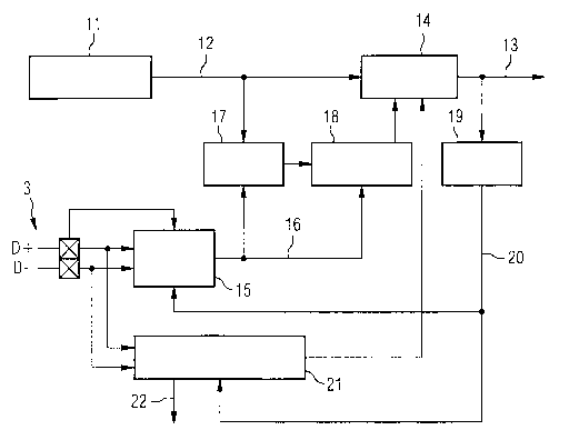
An accuracy in the data transfer rate of 0.25 % is required according to USB
specifications. In order to generate a clock signal, which renders this
accuracy possible, the invention enlists the use of a clock generator unit
that operates without quartz. The inventive clock generator unit comprises an
internal clock generator (11), a pulse counter (17), which is connected to the
internal clock generator (11), a pulse number memory (18), and a pulse filter
(14). The pulse counter counts the number of the internally generated clock
pulses between two pulses of the synchronization signal (16), which are
transmitted according to the USB specification. The difference between the
determined pulse number and a specified pulse number is evaluated and is used
for controlling the pulse filter (14) that suppresses pulses, thereby
resulting in the generation of a stabilized clock signal (13).


French Abstract

Les spécifications USB stipulent un niveau de précision des débits de transmission de données de l'ordre de 0,25 %. Afin de produire un signal d'horloge qui permette d'atteindre ce niveau de précision, il est prévu d'utiliser une unité génératrice d'horloge, fonctionnant sans quartz. L'unité génératrice d'horloge selon l'invention présente un générateur d'horloge interne (11), un compteur d'impulsions (17) relié au générateur d'horloge interne (11), une mémoire de nombre d'impulsions (18) et un filtre d'impulsions (14). Le compteur d'impulsions compte le nombre d'impulsions d'horloge produites à l'intérieur, entre deux impulsions du signal de synchronisation (16), qui sont transmises selon la spécification USB. La différence entre le nombre d'impulsions déterminé et un nombre d'impulsions théorique est évaluée et utilisée pour piloter le filtre d'impulsions (14) qui supprime des impulsions. On obtient ainsi un signal d'horloge (13) stabilisé.

Claims

Note: Claims are shown in the official language in which they were submitted.


claims
1. A clock generator unit having
- an internal clock generator (11; 31) which generates clock
pulses (12) at an internal clock frequency which is higher
than or equal to the nominal clock frequency of a stabilized
clock signal,
- a pulse counter (17) which is connected to the internal
clock generator (11; 31) and can be set to a start value by a
synchronization signal (16),
- a pulse number memory (18) which can store, as an actual
value, the number of clock pulses generated between preceding
pulses of the synchronization signal (16), and
- a pulse filter (14) which uses the number stored in the
pulse number memory (18) and a stipulated nominal number of
clock pulses to ascertain the number of pulses which need to
be filtered out of the generated clock signal (12), and which
filters the generated clock signal (12) such that a number of
clock pulses which corresponds to the nominal number can be
tapped off as a stabilized clock signal (13).
2. The clock generator unit as claimed in claim 1,
characterized in that the pulse number memory (18) contains
the number of clock pulses generated between two preceding
pulses of the synchronization signal (16).
3. The clock generator unit as claimed in claim 1,
characterized in that the pulse number memory (18) contains an
average number of clock pulses generated between a plurality
of preceding pulses of the synchronization signal (16).
4. The clock generator unit as claimed in claim 1,
characterized in that the synchronization signal (16) is
ascertained from an input signal (3) by a synchronization
-8-

decoder (15), and the stabilized clock signal (13) is
connected to the synchronization decoder (15).
5. The clock generator unit as claimed in claim 1,
characterized in that the synchronization signal (16) is the
synchronization signal provided in accordance with the USB
specifications.
6. The clock generator unit as claimed in claim 1,
characterized in that the stabilized clock frequency (13) at
the output of the pulse filter (14) is higher, in an even-
numbered ratio, than the required nominal frequency of an
operating clock signal (20), with a frequency divider (19)
being provided which generates the operating clock signal (20)
by division from the stabilized clock signal (13) at the
output of the pulse filter (14).
-9-

Description

Note: Descriptions are shown in the official language in which they were submitted.


CA 02419260 2003-02-11
P2000,0190
Description
Clock generator, particularly for USB devices
The invention relates to a clock generator unit which is used
particularly in connection with USB devices. In accordance
with the USB specification, a particular accuracy needs to be
observed for the data transmission rates. In full speed mode,
an accuracy of ~ 0.25% is required. This accuracy can be
achieved only through the clock accuracy; the clock used
therefore also needs to have this high level of accuracy.
However, the USB bus contains no explicit clock line. Each
device therefore needs to be able to generate the clock
itself. If the accuracy for the clock signal is not achieved,
then the device is not USB compatible.
Clock signals are normally generated using a circuit on a
chip, with an accuracy of ~ 3% being able to be achieved. To
increase the accuracy, it is known practice to use an
additional crystal. Such crystal oscillator circuits are
known, by way of example, from "Tietze, Schenk: Halbleiter-
Schaltungstechnik [Semiconductor circuitry], Springer Verlag
1999, 11th edition, pages 910 ff.". In this case, the crystal
module is in the form of an external component. For many
applications, however, it is necessary or desirable for all
the modules to be on one chip. When using an external crystal,
one or two additional pins are required on the chip, which is
generally undesirable and generates additional cost. Another
problem is the size of a crystal, since in chip cards, for
example, a thickness of 800 ~m is not meant to or cannot be
exceeded. With a crystal, these specifications cannot be
observed.
-1-

CA 02419260 2003-02-11
It is therefore an object of the invention to specify a clock
generator unit which generates clock signals with a
particularly high level of accuracy but nevertheless does not
require a crystal module.
This object is achieved by a clock generator unit having
- an internal clock generator which generates clock pulses at
an internal clock frequency which is higher than or equal to
the nominal clock frequency of a stabilized clock signal,
- a pulse counter which is connected to the internal clock
generator and can be set to a start value by a synchronization
signal,
- a pulse number memory which can store, as an actual value,
the number of clock pulses generated between preceding pulses
of the synchronization signal, and
- a pulse filter which uses the number stored in the pulse
number memory and a stipulated nominal number of clock pulses
to ascertain the number of pulses which need to be filtered
out of the generated clock signal, and which filters the
generated clock signal such that a number of clock pulses
which corresponds to the nominal number can be tapped off as a
stabilized clock signal.
The way in which the inventive clock generator unit works is
based on a synchronization pulse being transmitted, in
accordance with the USB specifications, at regular intervals,
for example every millisecond in full speed mode, with the
frequency of this synchronization signal having a much higher
level of accuracy than the required data transmission rate.
The fixed interval between the pulses of the synchronization
signal and the desired nominal frequency are taken as a basis
for stipulating how many clock pulses the clock generator
-2-

CA 02419260 2003-02-11
needs to generate between two pulses of the synchronization
signal. By comparing the nominal number of pulses with the
actual number of pulses between two preceding synchronization
pulses, it is known how much the actual clock frequency
differs from the nominal clock frequency. By filtering out
excess pulses from the internally generated clock signal, the
actual clock frequency can be reduced to the necessary nominal
clock frequency.
In one advantageous refinement, not only is the number of
pulses between two preceding synchronization signals
evaluated, but also an average is formed between a plurality
of periods. This allows the frequency's range of fluctuation
to be reduced further.
One advantage is that the inventive clock generator device is
independent of parameters such as technology, temperature or
power consumption. It is therefore possible to dispense with
expensive measures for observing manufacturing tolerances.
In accordance with the USB specifications, the accuracy of the
synchronization signals is higher by a factor of more than
five than the accuracy of the stabilized clock frequency
required. As a result, a sufficiently large scope for change
is left for tuning the components.
For the accuracy, it is also advantageous if the stabilized
clock signal is an internal stabilized clock signal whose
frequency is higher, in an even-numbered ratio, than the
nominal clock frequency of an operating clock signal. In this
case, a frequency divider is provided which generates the
operating clock signal at the prescribed nominal clock
frequency from the internal stabilized clock signal.
-3-

CA 02419260 2003-02-11
A further advantage arises if the pulse memory's value and/or
the output signal from a synchronization decoder and/or the
output signal from a signal decoder are fed back to the
internal clock generator and this allows the frequency of the
internal clock generator to be readjusted.
Other details and refinements of the invention are specified
in the subclaims.
The invention is explained in more detail below with reference
to an exemplary embodiment. In the drawing:
figure 1 shows the connection between two devices based on the
USB standard,
figure 2 shows a first, simple exemplary embodiment of a clock
generator unit in the form of a block diagram, and
figure 3 shows a second, extended exemplary embodiment of the
clock generator unit from figure 2, likewise in the form of a
block diagram.
A USB connection is provided, as shown in figure l, between
two devices, one of them being referred to as the USB host 1
and the other being referred to as the USB device 2. The role
of the USB host 1 is taken on by a PC or a HUB, for example.
It is likewise possible for a HUB or, by way of example, a
keyboard, a mouse, a scanner or a chip card to be used as the
USB device 2. Besides a 5 volt connection and a ground
connection, two data lines D+ and D- are provided. Via the two
data lines D+ and D-, the data traffic runs between the USB
host 1 and the USB device 2. Depending on the magnitude of the
power requirement for the USB device 2, voltage is supplied by
-4-

CA 02419260 2003-02-11
means of the bus connection or by means of a separate voltage
supply.
In accordance with the USB specifications, a clock line is not
provided. It is therefore necessary for each USB device to
have a separate clock generator which, as stated in the
introduction to the description, needs to satisfy high demands
on accuracy. To synchronize the data traffic between the USB
host 1 and the USB device 2, the USB host 1 sends a
synchronization signal at an interval of 1 ms in full speed
mode. This synchronization signal has an accuracy of 0.05% in
full speed mode.
Figure 2 now describes a clock generator unit for a USB device
2 which utilizes the incoming, highly accurate synchronization
signals to manipulate an internally generated clock signal in
order to achieve the necessary degree of accuracy for the data
transmission rate.
An internal clock generator 11 generates an unstabilized clock
signal 12 whose frequency is higher than a desired stabilized
frequency. To get from the unstabilized clock signal 12 to a
stabilized clock signal 13, a pulse filter 14 suppresses
individual pulses. To obtain the information regarding how
many pulses need to be suppressed, the number of pulses of the
unstabilized clock signal 12 which are generated between two
pulses of the synchronization signal 16 is counted and is
compared with a nominal pulse number.
A synchronization decoder 15 decodes the synchronization
signal 16 from an input signal 3 on the data lines D+ and D-.
The pulses of the synchronization signal 15 reset a pulse
counter 17. This is subsequently incremented by the pulses of
the unstabilized clock signal 12. At the same time as the
-5-

CA 02419260 2003-02-11
pulse counter 17 is reset, the present counter reading is
written to a pulse number memory 18. The value in the pulse
number memory thus describes the number of clock pulses 12
which have been generated between two preceding
synchronization pulses 16. The pulse number memory 18 is
connected to the pulse filter 14, so that the pulse filter 14
can evaluate the magnitude of the difference between the
nominal pulse number and the pulse number generated in the
last period. This number of pulses is then filtered out of the
internal clock signal 12. If the clock frequency of the
internal clock generator 11 remains the same during two
synchronization signal periods, the frequency at the output of
the pulse filter 14 thus corresponds exactly to the nominal
frequency in the second period.
In one beneficial form, the output signal from the pulse
filter 14, that is to say the stabilized clock signal 13, is
much higher than the required clock signal 20 and is in an
even-numbered ratio therewith. A frequency divider 19 then
obtains the ultimately needed operating clock signal 20; at
USB full speed its frequency is 12 MHz. The nominal frequency
for the stabilized clock signal would then be 48 MHz if the
frequency divider 19 is implemented in a ratio of 4:1. The
operating clock signal 20 at 12 MHz is then supplied to the
synchronization decoder 15 and to a data signal decoder 21.
To clarify the invention, the numerical example started above
will be taken further. If the frequency of the unstabilized
clock signal 12 has an upward discrepancy of 3%, then the
frequency generated is 49.44 MHz. During a synchronization
signal period of 1 ms, 49 440 clock signals are thus
generated, while the nominal clock pulse number is 48 000, in
line with 48 MHz. Accordingly, 1 440 pulses need to be
suppressed, advantageously at the same intervals. In this
-6-

CA 02419260 2003-02-11
case, approximately every 34th pulse would therefore be
filtered out.
The data signal decoder 21 then uses the nominal clock
frequency of 12 MHz to decode the input signal 3 applied via
the lines D+ and D-, and outputs it as a decoded output signal
22 for further processing.
Data are naturally likewise sent using the same stabilized
clock frequency of 12 MHz.
In the extended exemplary embodiment shown in figure 3, an
internal clock generator 31 is in a readjustable form. Using
the synchronization signal 16 and the value stored in the
pulse number memory 18 or using an output signal from the data
signal decoder 21, the frequency generated by the internal
clock generator 31 is trimmed. This means that the differences
between the unstabilized clock signal 12 and the stabilized
clock signal 13 are much smaller from the outset.
Another way of improving the control response involves not
only evaluating the number of pulses in a preceding
synchronization signal period, but also forming an average
between a plurality of preceding periods. This means that the
extreme values arising for the pulse number are much smaller.
The invention is naturally not limited to USB full speed mode,
but can also be used in low speed mode. However, the required
accuracy in this case is 1.5%, which is much simpler to
attain.
In addition, the invention can be applied to other
applications, provided that a sufficiently accurate
synchronization signal is available.

List of references
1 USB host
2 USB device
CA 02419260 2003-02-11
3 Input signal
11; 31 Internal clock generator
12 Unstabilized clock signal
13 Stabilized clock signal
14 Pulse filter
15 Synchronization decoder
16 Synchronization signal
17 Pulse counter
18 Pulse number memory
19 Frequency divider
20 Operating clock signal
21 Data signal decoder
22 Output signal
-11-

Representative Drawing
A single figure which represents the drawing illustrating the invention.
Administrative Status

2024-08-01:As part of the Next Generation Patents (NGP) transition, the Canadian Patents Database (CPD) now contains a more detailed Event History, which replicates the Event Log of our new back-office solution.

Please note that "Inactive:" events refers to events no longer in use in our new back-office solution.

For a clearer understanding of the status of the application/patent presented on this page, the site Disclaimer , as well as the definitions for Patent , Event History , Maintenance Fee  and Payment History  should be consulted.

Event History

Description Date
Inactive: IPC from MCD 2006-03-12
Application Not Reinstated by Deadline 2005-08-22
Time Limit for Reversal Expired 2005-08-22
Deemed Abandoned - Failure to Respond to Maintenance Fee Notice 2004-08-23
Letter Sent 2003-05-02
Inactive: Correspondence - Transfer 2003-04-11
Inactive: Courtesy letter - Evidence 2003-04-01
Inactive: Cover page published 2003-03-31
Letter Sent 2003-03-27
Inactive: Acknowledgment of national entry - RFE 2003-03-27
Application Received - PCT 2003-03-15
Inactive: Single transfer 2003-03-12
All Requirements for Examination Determined Compliant 2003-02-11
Request for Examination Requirements Determined Compliant 2003-02-11
National Entry Requirements Determined Compliant 2003-01-08
Application Published (Open to Public Inspection) 2002-02-28

Abandonment History

Abandonment Date Reason Reinstatement Date
2004-08-23

Maintenance Fee

The last payment was received on 2003-08-06

Note : If the full payment has not been received on or before the date indicated, a further fee may be required which may be one of the following

  • the reinstatement fee;
  • the late payment fee; or
  • additional fee to reverse deemed expiry.

Patent fees are adjusted on the 1st of January every year. The amounts above are the current amounts if received by December 31 of the current year.
Please refer to the CIPO Patent Fees web page to see all current fee amounts.

Fee History

Fee Type Anniversary Year Due Date Paid Date
Basic national fee - standard 2003-02-11
Request for examination - standard 2003-02-11
Registration of a document 2003-03-12
MF (application, 2nd anniv.) - standard 02 2003-08-21 2003-08-06
Owners on Record

Note: Records showing the ownership history in alphabetical order.

Current Owners on Record
INFINEON TECHNOLOGIES AG
Past Owners on Record
MICHAEL BRUHNKE
UWE WEDER
VIKTOR PREIS
Past Owners that do not appear in the "Owners on Record" listing will appear in other documentation within the application.
Documents

To view selected files, please enter reCAPTCHA code :


To view images, click a link in the Document Description column. To download the documents, select one or more checkboxes in the first column and then click the "Download Selected in PDF format (Zip Archive)" or the "Download Selected as Single PDF" button.

List of published and non-published patent-specific documents on the CPD .

If you have any difficulty accessing content, you can call the Client Service Centre at 1-866-997-1936 or send them an e-mail at CIPO Client Service Centre.


Document
Description 
Date
(yyyy-mm-dd) 
Number of pages   Size of Image (KB) 
Description 2003-02-10 8 313
Representative drawing 2003-02-10 1 6
Claims 2003-02-10 2 64
Drawings 2003-02-10 2 22
Abstract 2003-02-10 1 26
Acknowledgement of Request for Examination 2003-03-26 1 185
Notice of National Entry 2003-03-26 1 225
Reminder of maintenance fee due 2003-04-22 1 107
Courtesy - Certificate of registration (related document(s)) 2003-05-01 1 107
Courtesy - Abandonment Letter (Maintenance Fee) 2004-10-17 1 178
PCT 2003-02-10 4 139
PCT 2003-02-11 4 206
Correspondence 2003-03-26 1 24
PCT 2003-02-11 4 170