Note: Descriptions are shown in the official language in which they were submitted.
CA 02420681 2003-02-25
WO 02/19550 PCT/USO1/27188
IMPROVED DIGITAL-DATA RECEIVER
SYNCHRONIZATION METHOD AND APPARATUS
STATEMENT AS TO RIGHTS TO
INVENTIONS MADE UNDER FEDERALLY
SPONSORED RESEARCH AND DEVELOPMENT
This invention was made with United States Government support awarded by
the United States Department of Energy under contract to UT-Battelle, LLC. The
United States has certain rights to this invention.
FIELD OF THE INVENTION
The current invention relates generally to digital-data receivers, and
particularly
to an improved digital-data receiver using multiple cross-coupled
synchronization
loops.
BACKGROUND OF THE INVENTION
1. Field of the Invention
Most digital transmitter devices utilize separate frequency-reference sources
(e.g., crystal oscillators, SAW resonators, etc.) to determine the various
parameters of
transmission such as RF carrier frequency, data-transmission bit (baud) rate,
data-burst
timing, and interface data rates (e.g., serial data input speeds). Even in
frequency-
synthesized units, one or more crystals are invariably used to set not only
the carrier
center frequencies, but also channel step sizes and the life. In digital
systems
incorporating data-acquisition functions, the required A/D converters are
often run at
independently selected rates dictated by the specific application.
Additionally, in the
typical modern system implementations employing embedded microprocessors or
microcontrollers, there is also a separate clock used to drive the processor
which is
based on the chip's instruction-cycle times.
As a result, there are usually a multiplicity of relatively unrelated clocks
runung in the unit which can generate varying levels of mutual interferences
due to the
"beat" or difference in frequencies between the sources. This problem can be
particularly troublesome when clock signals cross-couple via capacitive or
radiating
means into sensitive low-level analog signal inputs, synthesizer loop-control
lines
CA 02420681 2003-02-25
WO 02/19550 PCT/USO1/27188
2
(causing spurious RF emissions), or modulation-signal wiring (causing
modulation
noise, instabilities, or nonlinearities).
Interestingly, the solution to the aforementioned problem of multiple
unrelated
cloclcs and the resultant variable noise and "beat" interactions - fully
synchronous
system clocl~ing -can also produce a major performance benefit in the
implementation
of digital data receivers for lower-quality channels. Since virtually all data
streams are
organized with integrally related numbers of data bits, words, frames, and
burst lengths,
the fixed, well defined relationships between these rates or frequencies can
be exploited
to provide additional mechanisms to achieve faster and more robust
synchronization to
these components, both in acquisition and tracl~ing contexts.
2. Descr iption of Related Art
There are a large number of patents, textbool~s, and articles in the
literature
devoted to the general subject of phase-loclced loop (PLL) technology. There
have been
dozens of patents issued on various aspects of the PLL, including a variety of
circuits
for loop phase detection, both analog and digital in implementation. The
particular
aspect of PLL technology considered herein is the performance of PLLs in
receiver
syncluonization, especially in the noisy or distorted-channel conditions
(e.g.,
interference, fading, and/or multipath scenarios) which are far more
characteristic of
real RF linlcs than the highly idealized case of simple additive white
Gaussian noise
(AWGN). Invariably, RF circuits are initially analyzed for their performance
in a pwe
AWGN channel due to the simpler (statistical) mathematics; see, for example,
Digital
Communicatiofas, Third Editi~~z, by John G. Proaltis, 1995. The performance
(i.e., bit
euror rate versus signal-to-noise ratio) of most demodulators in fading and
multipath
(dispersive) environments is substantially worse than in pure-AWGN channels,
is much
more difficult to analyze, and in practice requires significantly more finesse
to achieve
good linlc performance. Indeed, most of the mathematical simulations of fading
channels are made assuming perfect receiver synchronization is somehow
achieved;
unfortunately, this in reality is unjustifiably optimistic. At low signal-to-
noise ratios
(SNRs), synchronization quality can become a dominant factor in the overall
receiver
bit error rate (BER) performance level. Thus, improved methods of receiver
synchronization for use in poorer-grade RF communications channels are needed
to
elevate wireless system BER performance levels, provide more uniform coverage
CA 02420681 2003-02-25
WO 02/19550 PCT/USO1/27188
3
(particularly in rough terrain), and accommodate greater numbers of users. A
survey of
the existing patent art will further clarify this need.
U. S. Patent 4,091,331, issued May 23, 1978 to Hans-Peter Kaser, et al,
discloses a method to compensate RF carrier phase errors by tracking the
carrier with a
feedback loop incorporating a phase-error predictor. A means for optimizing
the gain of
the phase-estimator loop circuit is provided by processing the successive bit-
by-bit
residual phase eiTOrs (~~",~~n+1) . This patent describes an adaptive-gain
algorithm
to optimize the phase tracking of a receiver during changing reception
conditions,
where the ratio of carrier phase fitter to Gaussian noise is varying due to
dynamic RF
transmission channel characteristics. If successive phase-error variance
samples are
uncorrelated (i.e., avg[Df",Df"+1]-0) the loop gain is optimum; if the
correlation result
is >0, then the loop gain must be increased; and if the correlation is <0, the
gain must
be reduced. This patent clearly does not describe multiple interconnected
phase
detectors or PLLs; it therefore has no bearing on the instant invention.
U. S. Patent 5,251,237, issued Oct. 5, 1993 to Alfred Baier, discloses a
method
of dynamic channel data-quality assessment principally using measurements of
the
channel impulse response and the total power therein to estimate the degree of
dispersion in the time-multiplexed European "GSM" cellular-phone link. The
effective
dispersion time of the multiple reflected signals is computed, as is the time
distribution
of the total slot signal power. From this estimate, parameters of adaptive
equalizers
and/or maximum-likelihood (Viterbi-type) data decoders are adjusted to provide
acceptable BER performance. To conserve power in battery-operated cell-phone
transceivers, the degree of signal processing is dynamically minimized; when
the
channel is good, the extra processing hardware is switched off to extend
battery life.
This scheme is directed solely at time-division multiplexed systems (e.g.,
GSM) and is
not broadly applicable to other types of systems such as spread-spectrum.
Further, this
patent makes no mention of PLL-based systems (single or multiple) and has no
applicability to synchronization methods. Thus there is no commonality with
the instant
application.
U. S. Patent 5,367,536, issued Nov. 22, 1994 to Ichiro Tsujimoto, describes a
method in time-division multiple-access (TDMA) systems of transmitting
concurrent
sync and data bursts by differentially encoding the data to produce a spectral
null near
CA 02420681 2003-02-25
WO 02/19550 PCT/USO1/27188
4
the RF carrier when modulated; conversely, the more bandlimited sync burst is
directly
modulated onto the Garner and thus occupies the spectral region immediately
straddling
the carrier frequency. Since the sync and data signal spectra are not
overlapping, the
receiver can separate out the sync components via a simple bandpass filter and
recover
a clean data-clock therefrom. In parallel, the data signal is corrected by a
standard
decision-feedbacl~ equalizer to filter out the sync components and
subsequently
demodulated; timing for these latter operations is obtained from the recovered
sync-
derived cloclc. This patent, although useful for its intended applications,
does not
involve any type of PLL circuitry and clearly employs very conventional
techniques for
extracting data clocl~ from the received sync burst. No use of multiple PLL
detectors or
loops is mentioned. There is thus no overlap with the instant invention.
U. S. Patent 5,838,741, issued Nov. 17, 1998 to Edgar Callaway, Jr. et al,
discloses a scheme that ensures that digital data in an RF receiver is
transferred to
downstream stages only at times which will have minimal impact (e.g., from
radiated
or conducted noise) on the front-end and other more sensitive parts of the
circuit. The
scheme is generally applicable to miniature units and particularly relevant to
single-
chip (monolithic) devices. The salient goal is to minimize on-chip data
transfers (with
their inherent noise) during any critical signal-sampling instants, delaying
them to less
sensitive times. The system controller can be configured to insert an optimum
delay
into the various subsystem control lines to avoid logic transitions at noise-
critical times
for the various circuits. Although the techniques herein are useful for the
manufacture
of receiver hardware, they only deal with noise generated internal to the
receiver itself
and do not in any way address RF link noise and degradations affecting the
input signal
from the antenna. Thus this patent and the instant invention deal with totally
different
problems and therefore are not intersecting in scope.
U. S. Patent 5,832,045, issued Nov. 3, 1998 to Andrew Barber, discloses a
method and apparatus to adjust data-bit (baud) timing through a correlation
assessment
of intersymbol interference (ISI) induced by imperfections in the data line.
This patent
is directed at improved methods of generating baud (bit) timing for
applications such as
high symbol-rate data modems for telephone lines, where better precision in
establishing bit timing is critical to high data throughputs with low errors.
The
invention improves timing resolution over existing carrier-envelope detection
and
CA 02420681 2003-02-25
WO 02/19550 PCT/USO1/27188
simple bit-energy correlation methods by correlating successively adjacent
(irmnediately leading and trailing) bits to provide a simple but accurate
bipolar error
signal which is then used to adjust the timing of the bit sampler wluch drives
the
correlators. This "early-late" scheme is similar in concept to spread-spectrum
5 polynomial correlators widely employed in direct-sequence systems, but here
simply
functions as the phase-error detector in a conventional PLL setup. The
application of
this technique is never extended to recovering multiple clocl~ frequencies,
nor is the use
of interconnected loops cited. Thus again, there is no commonality with the
specifics of
the instant case.
U. S. Patent 5,825,805, issued Oct. 20, 1998 to Ichiro Nato, describes a
spread-
spectrum modulation/demodulation technique similar to the orthogonal frequency-
division multiplex (OFDM) scheme used in European DV-B digital television
transmission. The inventor claims the advantage of very rapid synchronization
of the
code at the receiver by matching the frequency-spreading pattern, but the
patent
discloses no specific PLL circuits or detectors to recover sync information;
indeed, an
advantage is cited in that existing-art sync and data demodulators can be
utilized on the
despread output streams. Thus, again, there is no overlap with the subject of
the instant
application.
U. S. Patent 5,493,583, issued Feb.20, 1996 to Peter Cripps, discloses a
wireless
transceiver architecture employing a PLL-based frequency-multiplier to
generate the
transmit carrier. The salient feature of the system is a means of rejecting
simultaneously transmitted data in the same unit's receiver by subtracting a
portion of
the transmitted data bitstream from the received stream after demodulation to
minimize
transmitter-to receiver crosstallc. However, no use of multiple and/or
crosscoupled
PLLs is mentioned, and no synchronization functions other than common art are
included. There is once more no conflict with the instant invention.
U. S. Patent 3,633,115, issued Jan. 4, 1972 to Marvin Epstein, is a
fundamental
patent predating the chip-type PLL which discloses a means of following the
average
phase of an input clocl~ signal for smoothing timing within a logic system.
The PLL
error signal is heavily filtered to ignore rapid phase variations or fitter in
the input
signal but faithfully traclc long-term trends. This concept, while
incorporated in nearly
all modern PLL implementations, is clearly in the public domain.
CA 02420681 2003-02-25
WO 02/19550 PCT/USO1/27188
6
U. S. Patent 4,780,891, issued Oct. 25, 1988 to Jean-Pierre Guerin et al,
describes a method and apparatus to approximately phase-synchronize two
digital
bitstreams by using the later as a reference and inserting a programmable
logic-
generated delay (within a selectable control window) into the path of the
earlier-
arriving stream. This technique does not employ any PLL hardware and thus is
not
relevant to the instant case.
U. S. Patent 3,491,338, issued Jan. 20, 1970 to Francis Malloy, discloses a
receiver data synchronizer built around adjustable multivibrator timing
elements. A
predetermined multi-bit preamble is sent with each data burst to facilitate
proper
decoding and to provide discrimination against atmospheric noise. Adjustment
of the
system is essentially manual, and no PLL or other automatic correction
mechanism is
included.
U. S. Patent 5,519,444, issued May 21, 1996 to Yong I~o et al, discloses a
phase-synchronizing apparatus for digital audio signals in digital-video
applications
. which regenerates a data transmission clock using a PLL topology. The
various
selectable clock-frequency sets (keyed to the standard 48-, 44.1-, and 32-l~Hz
audio
sampling rates) are generated from edges of the input digital-audio data
pulses and two
groups of programmable PLL-type frequency dividers, one driven by a 21.333-
lcHz
master reference clock and the other by an 18.432-kliz source. By selection of
a
multiplicity of the internal divide ratios, all the needed bit, frame, and sub-
sampling
rates for the 3 standard-rate digital audio streams can be generated. The two
PLL
systems are merely synthesizers and are cascaded to produce the desired
frequencies,
but they are not interconnected or used in an RF receiving function as in the
systems of
the instant invention.
U. S. . Patent 3,341,658, issued Sep. 12, 1967 to Hisashi Kanelco, discloses a
matched-filter/correlator synchronization system for an RF receiver. Tlus
early
development in correlation processing utilized tapped passive delay lines on
the input
and reference-waveform channels; the two signal sets were multiplied point-by-
point
and the sum used to correlate the received Barker-sequence encoded sync word
with
the identically encoded reference. At the peak of the correlation sum, the
sync timing is
probabilistically optimized, even in the presence of significant amounts of
Gaussian
noise. This patent, now obviously in the public domain, does not utilize
multiple or
CA 02420681 2003-02-25
WO 02/19550 PCT/USO1/27188
7
interconnected PLLs of any bind and therefore does not impinge on the instant
invention.
U. S. Patent 4,545,061, issued Oct. 1, 1985 to Ronald Hileman, describes means
for maintaining close receiver time synchronization in spread-spectrum and
other
correlation-type communication systems, even in low-SNR conditions. The basic
sequence-correlation loop is equipped with a dithered local oscillator whose
phase is
perturbed periodically; the resulting dither modulations on the heterodyned
received
signal are coherently detected in a switched phase-inverter run at the same
dither rate.
The resulting dither-sideband energy is sent to two antiphase high-Q
resonators, which
are subsequently amplitude-detected in a diode bridge and low-pass filtered.
The
resulting bipolar error signal is then used to adjust the local correlator
clocl~, which in
turn traclcs the received sequence phase and thereby achieves synchronization
with
what is conventionally l~noml as a "tau-dither" loop. Since only one PLL is
utilized,
this patent does not relate to the instant case.
U. S. Patent 5,402,450, issued Mar. 28, 1995 to Gary Lennen, discloses a
complex scheme to subtract out multipath-induced errors from the satellite-
based
positioning signals received in a GPS receiver. In general, good multipath
rejection is
difficult to achieve except in spread-spectnun or other dispersive
communications
systems; even in these formats, multipath causes noticeable degradations in
overall
system performance. Succinctly, tlus technique is based on an understanding of
the
autocorrelation function (AF) of a spread-spectrum signal. In an ideal case,
the AF is
triangular when plotted against code-signal delay. The presence of multipath
components in the received signal distorts and delays the pear of the AF (best
correlation point), which causes an error when the AF is employed in a delay-
loch loop
(a form of PLL) to measure the precise code phase (and thus the pseudorange)
from a
GPS satellite. Although the implementation incorporates multiple delay-loch
loops,
they are operated in parallel and employ individual detectors for each loop;
as a result,
this patent does not overlap with the instant invention.
Finally, U. S. Patent 5,739,727, issued Apr. 14, 1998 to Bjorn Lofter, et al,
discloses a sampled PLL being loclced with support from another (standard)
PLL. The
application is in a programmable frequency synthesizer which is desired to
have fast
switching and settling times and simultaneously exhibit low phase noise in the
locl~ed
CA 02420681 2003-02-25
WO 02/19550 PCT/USO1/27188
8
condition. Since in conventional PLL circuits, a fast response time requires a
large
control-signal bandwidth, this constraint is directly at odds with a low phase-
noise level
(requires heavy control-signal filtering and thus low bandwidth). The solution
in this
patent is, after switching the synthesizer to a new frequency, to pre-set the
main PLL's
initial frequency (using a fast digitally-sampled auxiliary PLL) to the
desired value,
thus affording rapid switching. To maintain the desired low phase noise, the
main-PLL
control voltage is severely filtered to limit its bandwidth; now that the main
PLL
control voltage is preset by the "helper" circuit to very close to its desired
final value,
the slow main-loop response will not degrade the system's overall
switching/settling
time specs. This concept, however, does not address receiver applications or
multiply-
interconnected PLLs; thus it is completely distinct from the instant
invention.
While each of the foregoing may have some utility for the intended
applications
thereof, none of them directly address or effectively solve the problems noted
initially
above. For these reasons, there still remains room for improvement in the art.
SUMMARY OF THE INVENTION
It is an object of this invention to provide an improved digital-data receiver
apparatus and method.
It is another object of this invention to provide a digital-data receiver
apparatus
and method wherein frequency and phase errors are minimized.
It is an object of this invention to provide a digital-data receiver and
method
having a synchronous design such that all internal reference frequencies are
driven
from a common source.
It is another obj ect of this invention to provide a digital-data receiver and
method in which problems associated with multiple "beat" components are
eliminated.
It is a fuxther object of this invention to provide a digital-data receiver
and
method in which all clock frequencies are integrally or fractionally related.
It is an even further object of this invention to provide a digital-data
receiver
and method in which the variable beat-rate pattern noise modulations within
the system
no longer occur.
It is an even further object of this invention to provide a digital-data
receiver
and method which exploits timing redundancies inherent in a typical data
stream to
concurrently but independently provide robust synchronization to all lcey
frequencies
CA 02420681 2003-02-25
WO 02/19550 PCT/USO1/27188
9
embedded in the stream (i.e., bit, word, frame, burst rates) as well as
related modulation
(e.g., spread-spectrum chipping rates) and transmission (RF carrier frequency)
parameters, even in poor communication channels.
It is an even further object of this invention to provide a digital-data
receiver
and method which results in a lower sustained bit-error rate in adverse
receiving
conditions by maintaining synchronization during intervals of degraded signal
quality
when conventional systems would fail.
It is an even further object of this invention to provide a digital-data
receiver
and method which results in a simpler lower-power logic design, lower gate
counts and,
thus, smaller chip areas and lower fabrication costs.
It is an even further object of this invention to provide a digital-data
receiver
and method for providing simplification of the related spread-spectrum
receiver system
hardware and improvement in its acquisitioulockup times, more reliable data-
burst
acquisition, and the facilitation of more robust receiver synchronization
methodologies
at the RF-carrier, chip, data-bit, frame, and burst levels.
It is a further object of this invention to provide a receiver in which the
phase
lock loop circuitry comprising synchronization loops for received data signals
are
mutually cross-coupled such that each loop is capable of providing to and
receiving
from each other loop a comparison or corrective signal with respect to
frequency and/or
phase, the comparison signal being used by the receiving loop to minimize or
eliminate
loss-of signal or degradation of signal events such as those caused by noise,
interference, signal fade, and the lilce.
These and other obj ects of the invention are achieved by an improved digital-
data receiver synchronization apparatus having a plurality of memory devices
for
receiving multiple timing signals; and a feedback means interconnecting the
memory
devices and cross-coupling signals produced by the memory devices; wherein the
receiver provides fast lock-up times and superior loss-of loclc protection in
moderately
to severely noisy conditions and has generally improved tolerances to clock
asymmetries and channel-induced timing fitter.
Another object of the current invention is a method of providing improved
digital-data receiver synchronization comprising the steps o~ providing a
plurality of
memory devices for receiving multiple timing signals, each of the plurality of
memory
CA 02420681 2003-02-25
WO 02/19550 PCT/USO1/27188
devices comprising a composite phase-frequency detector; and, interconnecting
the
memory devices with a feedback means for cross-coupling certain signals
produced by
the memory devices; wherein the receiver produces fast lock-up times in
moderately to
severely noisy conditions and avoids loss of lock in all but the most severe
fading,
5 interference, and/or multipath conditions.
These and other obj ects of the invention are also achieved by providing the
described apparatus and method, wherein a common or master frequency reference
source is used to provide timing signals to each of the memory devices.
Brief Description of the Drawings
10 Figure 1 provides block diagrams of three alternate forms of prior-art
digital-
data receiver clock synchronization.
Figure 2 is a block diagram of the basic functioning of the receiving system
of
the current invention.
Figure 3 is a schematic diagram of the interconnecting feedback logic
employed by the multiple phase-locked loops (PLLs) of the current invention.
Figure 4A & 4B is a schematic representation of the functioning of the
exclusive-OR (XOR) detector and phase-frequency detector components of the
current
invention.
Figure 5 is a schematic diagram representing the preferred embodiment of the
composite phase-frequency detectors of the current invention.
Figure 6 is a schematic representation of the functioning of the input-signal
noise suppression component of the current invention.
Figure 7 is a blocle diagram of a simplified embodiment of the current
invention
utilizing only a single VCO driven by a combination of three of the composite
phase-
frequency detectors.
Detailed Description of the Invention
The fundamental intent of the invention is, as described above, to exploit the
timing structure in a typical digital data transmission by concurrently and
corporately
synchronizing (locking) to each of the salient timing components in the data
stream.
When one or more of these components is corrupted by noise, multipatli,
interference,
or other channel degradations, the set of PLLs "fills in" the missing
synchronization
CA 02420681 2003-02-25
WO 02/19550 PCT/USO1/27188
11
information by regenerating the necessary signals) from a combination of the
remaining (uncorrupted) components.
While applicable to highly complex transmitter-receiver systems, the basic
principles of the current invention may be generally explained by reference to
a simple
system. For the sake of simplicity, a transmitter is assumed to emit three
types of data
related signals, each at a distinct frequency. These three signal-frequency
components
are the carrier, the data bit rate, and the data frame rate. A more complex
system, to
which the current invention is equally applicable, will also include
additional timing
signals such as the spread-spectrum chipping clock, transmission burst rate
and other
signals. These and other elements of a receiver are ignored for the purposes
of this
brief explanation.
A receiver for the transmitted data must simultaneously detect and match
("loclc
up" to) the frequencies (and, often, phases) of the carrier signal, the data
bit rate signal,
and the data frame rate signal. Currently, each of these signals will be at a
different
frequency derived from a clock means on the transmitter. In conventional
receivers,
clock means are required to generate timing signals to synchronize with each
data
signal such that the digital information may be extracted. Conventionally, the
various
clocks for these purposes are controlled by individual phase-locked loops
(PLLs). As
used herein, the term "phase-locked loop" or PLL is used to refer generally to
include
phase-locked loops, frequency-loclced loops, delay-lock loops, signal
correlators
(including but not limited to spread-spectrum correlation detectors), and
similar devices
as known by those of skill in the art. Each PLL must generate a frequency to
match or
synchronize with the received frequency, such that the transmitted digital
information
may be derived. The PLLs in the receiver must first synchronize with, or lock
up to,
the received signal, and then must maintain the timing pulses such that the
data may be
read as it is received.
In low signal-to-noise enviromnents, the initial loclcup time for a PLL may be
relatively long. Moreover, due to noise, interference, signal fading, and
other sources
of interference including those mentioned above, the lock may be lost and must
be re-
acquired. During periods of interference or noise, data is either not received
correctly
or is simply lost.
CA 02420681 2003-02-25
WO 02/19550 PCT/USO1/27188
12
Conventional efforts to overcome these problems include increasing the power
provided to the transmitter and/or receiver to increase the signal-to-noise
ratio, or to
add circuitry designed to condition the signals to improve acquisition or lock-
up times
and maintenance of the timing signal. Another solution basically requires the
transmitter to transmit for a longer period of time such that lock-up time and
signal loss
do not prevent the reception of the transmitted data. Each of these efforts
increases the
cost of the system and/or its individual components due to the increased power
requirements, increased complexity, and other incident factors.
One facet of the currently presented improvements for a digital-data receiver
involves the use of composite phase-frequency detectors (CPFDs) for each, or
as part of
each, synchronization loop or PLL. The CPFD provides corrections for phase,
frequency, or both, such that the operation of the PLL and hence the operation
of the
receiver is more robust.
In an additional aspect of the current invention, in relatively simple terms
described in more detail below, the current invention overcomes the problems
noted by
providing mutual cross-coupling circuitry for each PLL or synchronization
loop. In a
most preferred form, the cross-coupling and the CPFDs are utilized together to
achieve
a significantly more robust reception of data than has been possible to date.
The PLLs
are interconnected with analog, digital, and/or mixed type feedback signals to
cross
couple the respective error signals and output frequencies. The feedbaclc
provides a
corrective or comparison signal from each PLL to each other PLL or
synchronization
loop. The cross-coupling circuitry can, and typically will, comprise
conditioning
circuitry, such as frequency multipliers or dividers and phase adjustments, to
condition
the comparison signal appropriately for the synchrouzation loop to which it is
sent.
The cross-coupling, by providing a comparison signal, offers several
significant
advantages. The loclc-up time for each synchronization loop will be decreased
(lock-up
speed increased). Also, each loop will be enabled to more robustly maintain
the
acquired frequency loclc. The loop will therefore be able to function
efficiently even in
low signal-to-noise enviromnents. Moreover, random noise spikes or
interference can
be ignored. With these and. other advantages, power requirements are lessened
and
more complex conditioning circuitry is unnecessary. These advantages will be
CA 02420681 2003-02-25
WO 02/19550 PCT/USO1/27188
13
experienced in both the transmitter and receiver, thus reducing the costs,
sizes, aazd
complexities of transmitter/receiver systems.
The method and apparatus of the current invention may be used with both
asynchronous and synchronous transmitter/receiver architectures. Currently,
most
systems are asynchronous, that is, each transmitted data signal receives its
timing signal
from an independent frequency source or clock means. In this case, the cross-
coupling
circuitry for the comparison signals can comprise conditioning circuitry
whereby the
frequency of the comparison signal is at or near the nominal frequency of the
synchronization loop to which it is sent. Where the receiver is designed to
correspond
10~ to one, or a plurality of identical transmitters, this circuitry may be
hardwired. Where
the receiver is designed for use with differing transmitters, the conditioning
circuitry
may be hardware- or software-programmable such that it can be appropriately
varied.
The invention is most efficiently used with synchronous architecture, an
example of which is disclosed in co-pending application Serial No. 09/653,394,
assigned to the assignee of this invention. In a synchronous transmitter, each
component derives its timing signal from a single master cloclc, either
directly or
through simple multiplier or divider means. W a synchronous receiver, the
cross
coupling circuitry is greatly simplified, because each synchronization loop
derives its
timing signal from the master clock either directly or through simple
multiplier or
divider means.
The implementation of the current invention provides substantial advantages.
Power requirements can be reduced, as can circuit complexity. This provides
savings
in terms of both cost and the size of the components. Additionally, there are
significant
improvements in noise and interference rejection, effective system bit-error
rates, the
robustness of loclc-up to the incoming signal, and the speed of acquisition in
signal
lock-up. A more detailed description of the invention, with exemplary circuit
diagrams, is as follows.
Figure 1 of the drawings provides typical bloclc diagrams of receiver
synchronization architectures according to the current-art techniques. Figure
1(a)
shows a basic scheme with a multiple unrelated clocks; 1(b) illustrates a
single master
PLL/cloclc with downstream dividers to generate the secondary frequencies; and
1(c)
details three independent PLLs (one per frequency). Figure 2 of the drawings
is a
CA 02420681 2003-02-25
WO 02/19550 PCT/USO1/27188
14
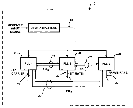
typical block diagram of the basic functioning of the receiving system 10 of
the current
invention. As shown in Figure 2, the receiving system 10 is designed to detect
three
distinct timing signals or frequencies of an input signal 20, such as the RF
caiTier f1 21,
the data bit (baud rate) f2 22, and the data frame rate f3 23. In many
instances there will
be a need for additional timing signals to be regenerated, including but not
limited to
the spread-spectrum chipping cloclc, transmission burst rate, epoch clocks,
and other
timing markers. For purposes of illustration, however, only the three
frequencies cited
above will be utilized.
In conventional receivers, various clocks are derived from individual phase-
locked loops (PLLs) or are derived from a single master loop synchronized to
the RF
carrier with downstream frequency-divider logic to generate the integrally
related data
and frame-rate clocks (Figure 1). However, there is little noise immunity
afforded
with this arrangement because any noise in the bandpass of the' data-modulated
RF
carrier signal will produce simultaneous fitter at all the derived clock
frequencies and
downstream phase-frequency detectors (PFDs) or other types of loop-phase
detectors in
the lower-speed derived loops.
To counter this effect, and concurrently provide faster loclc-up times in
moderately to severely noisy or distorted receiving conditions, the current
invention
provides a plurality of memory devices, for example PLLI 24, PLLZ 25, and PLL3
26
shown in Figure 2, which are mutually interconnected with bidirectional analog
or
digital feedbaclc signals f~" such as f~, 27, f~, 28, and f~, 29, to cross-
couple their
respective error signals and/or output frequencies. Each memory device (for
example,
PLL 24, PLL 25, and PLL 26) is driven by one common source or clock using edge-
triggered synchronous logic which generally affords improved tolerances to
clock
asymmetries, external EMI, propagation-delay variations, and supply and
temperature
changes. Additionally, the occurrences of random and varying-pattern digital
"glitches" coupling into critical signal, control, and RF lines are
significantly reduced.
Figure 3 is a schematic diagram of thel feedback logic employed by the PLLs
(for example, PLL 24, PLL 25, and PLL 26) of Figure 2. As illustrated in
Figure 3, the
preferred embodiment of the current invention incorporates a system of
multiple cross
coupled synchronization loops 30. The loops 30 include multiply-divide
feedback logic.
As such, fl 21, f2 22, and f3 23 are provided as precise integral (or
fractional) multiples
CA 02420681 2003-02-25
WO 02/19550 PCT/USO1/27188
or sub-multiples of each other with predetermined phase relationships. The
relationship of the signals fl 21, f2 22, and f3 23, as provided in a
preferred embodiment
of the current invention, is set forth below.
fl = M~fz = M~Nf3 (1)
5 f2 = N' f3 (2)
M=fl=f2 (3)
N=fi-fs (4)
Here, M and N are integers (in general, any positive rational numbers) limited
only in
practical applications by logic speeds, power, and phase-noise considerations.
Each
10 signal fl 21, f2 22, and f3 23 is then fed to its respective composite
phase-frequency
detector (CPFD), for example CPFD1 31, CPFDZ 32, and CPFD3 33, which measures
the overall phase and frequency error in each loop and provides a corrective
signal to
its associated voltage-controlled oscillator (VCO), for example VCO, 34, VCOZ
35,
and VC03 36. Crossfeed circuits CFIZ 37, CF23 38, and CF13 39 provide
conditioned
1 S analog control-voltage interconnects between the designated CPFD bloclcs.
These
crossfeeds are, in a preferred implementation, controlled by a pair of
computational
blocks, labeled "Noise Logic" 41 and "Lock Logic"42, which respectively
evaluate the
noise level of the key incoming signal components and assess the stability of
each
loop's error voltage. If the input noise to a given loop is excessive, the
Noise Logic
bloclc senses the condition, either via a simple input-signal amplitude
measurement, a
frequency fitter assessment (described below), a pulse-width limiting status
level, or
other means. The Lock Logic circuitry, meanwhile, senses the lock status of
each
related PLL via error-voltage measurements (also detailed below), evaluations
of the
PFD phase-pulse output signals, XOR-detector average-voltage monitoring,
frequency
2 5 j fitter characterizations, or other means.
For completeness, Figures 4A & 4B present is a schematic
representation of the functioning of the standard (prior art) exclusive-OR
(XOR) gate
phase detector and of the conventional phase-frequency detector (PFD) used
within the
current invention. The output of the XOR gate is low (output = 0) whenever an
input A
and input B are the same, i.e., either both "high" or both "low". This
operation may be
seen as in Table 1 below, where the logical equation is A o B=Z, Z being the
XOR
output.
CA 02420681 2003-02-25
WO 02/19550 PCT/USO1/27188
16
Table 1
Input A Input B XOR Outbut
0 0 0
0 1 1
1 0 1
1 1 0
The corresponding waveforms and operational details for the standard PFD-type
detector are also provided, for reference, for a commercial 74HC4046
integrated-circuit
chip.
Figure 5 is a schematic diagram representing the preferred embodiment of the
CPFD circuitry 50 utilized in, for example, CPFD, 31, CPFDZ 32, and CPFD3 33
as
they are shown in Figure 3. The CPFD circuitry 40 used in the cunent invention
incorporates a standard-format phase-frequency detector (PFD) circuit, but
augmented
to provide greatly improved noise immunity and to provide means for
introducing the
cross-coupled signals extracted from the other (here, two) loop detectors. The
system
shown possesses the familiar advantages of the classic phase-frequency
detector over
other types - namely, larger 0360°) tracking range, much improved loch,
pull-in, and
pull-out ranges, low average phase error in lock, rapid frequency acquisition,
and
freedom from harmonic-frequency loclcing. In addition, though, the CPFD
circuit 50 at
loch also exhibits the quite low loop-phase fitter and noise heretofore
reserved to
analog and XOR-type detectors.
A complete PLL subsystem particularly suitable for the RF receiver application
is included diagrammatically in Figure 5. The PLL is am electronic circuit for
locking
an oscillator, such as a VCO 51 in frequency and/or phase with an arbitrary
input signal
which is employed to track a carrier or synchronizing signal which itself may
vary in
frequency and/or phase with time. Performance of the PLL is dependent on the
circuit's ability to accurately control the frequency and phase of the VCO
output.
Reference inputs frl 52 and fr2 53 are provided to the CPFD at a memory
device(s),
preferably divide-by-two flip-flop 54 and flip-flop 55, respectively.
Typically, these
inputs are differential or opposite-phased; i.e., as from the main (Q) and
inverted (Q')
outputs of a flip-flop or square-wave oscillator (usually the loop VCO
itself). Variable-
frequency input fV 56 is introduced into the CPFD at noninverting comparator
57. From
CA 02420681 2003-02-25
WO 02/19550 PCT/USO1/27188
17
the comparator 57, the squared-up signal (still at f~) proceeds to a further
memory
device in the CPFD circuitry, preferably divide-by-two flip-flop 58. Upon
leaving the
flip-flop 58, the output (now at %Zf~) is provided to another type of gating
device, such
as digital multiplexer 59. Digital multiplexer 59, at the direction of the
"Noise" and
"Loclc" logic blocl~s, selects either %Zf~ or one of the same-frequency
digital references
from the other cross-coupled PLLs for input into the XOR gate 64 along with
frz 60
from flip-flop 55. The flip-flops 54 and 55 are configured to feed the XOR
gate 64 so
that the input waveforms both have a duty cycle of precisely 50% and are
presented in
the proper 90-degree phase relationship so that at loch the desired half scale
average
(DC) output level [V~~o] is generated on the loop capacitor CV~o 86. When the
CPFD is
locl~ed in, the positive transition of the reference input fr2 60 and the
multiplexer 59
output 62 are equal in frequency and have a phase difference of very nearly 90
degrees.
Under these conditions, the logic outputs of the logic bloclcs will be high,
causing the
XOR gate 64 output on line 66 to be switched through SWl 81 to resistor Rl 82
and
thence to the output of the CPFD 85. Under lock, the duty cycle of the XOR
output 66
will be 50% and the output frequency will be equal to twice the input
frequency. Any
change in phase will result in a linear (but small) change in duty cycle,
until the loop is
rebalanced.
The output 68 from flip-flop 54 and multiplexer 59 are also provided to a
standard (but augmented) phase-frequency detector 70. PFD 70 provides both an
output
72 and a phase-pulse signal 74. Phase-pulse signal 74 is provided to a pulse-
width
limiting device, such as a gated delay generator; this could be either a
counter, a
standard monostable multivibrator ("one-shot"), or another implementation. In
a
preferred embodiment of the current invention, the standard PFD circuit is
augmented
by a one-shot 76 which is fed from the phase-pulse output 74 of the phase-
frequency
detector circuit 70. A negative-going phase pulse is generated in the
conventional PFD
70 (e.g., as incorporated in a type 74HC4046 CMOS PLL chip) to indicate when
the
main detector 70 pulses (both positive and negative) are generated and applied
to the
output pin 72 and thence to the loop filter capacitor C~~o 86, which in turn
integrates the
current pulses and stores the VCO loop error voltage.
Alternatively, the logic "high" intervals of this signal 74 can be viewed as
an
indicator of the "tri-state" cutoff condition of the main output between
pulses. The PFD
CA 02420681 2003-02-25
WO 02/19550 PCT/USO1/27188
18
70 is an edge-triggered device and is therefore more susceptible to untimely
short noise
pulses than the lower-performance XOR detector (64), which tends to average
them
out. The one-shot 76 serves to limit the output pulse widths applied to the
loop
capacitor C,,~o 86 and thus, once the Ioop is loclced, "blanks out" the
detrimentally Iong
pulses normally produced by the standard PFD circuit in response to input-
signal noise
spires.
To maintain stable loop loci during the noise intervals, the PFD output at 74
is
combined via resistive current summing through RZ 84 at node 85 with the
square-wave
output from XOR detector 64 through Rl 82. Switch SWZ 80 is provided to
disable the
output of the CPFD circuitry when a large noise spire is received which.would
threaten
the locred state of the circuit. The logic driving switch SWz 80 detects any
loss of loop
loclc; if so, the output of the PFD 72 is disconnected from the control node
85. Switch
80 thus operates to protect the local VCO (as well as the cross-connected PLL
circuits)
from being disturbed by noise spires by providing a holding action on the loop
control
voltage during noise intervals and thereby avoiding even a transient loss of
lock. The
filtered output from XOR 64 then "bridges through" noise pulses and lceeps the
loop
tightly controlled while the potentially unstable phase-frequency detector 70
signals are
switched out by 80 until the noise subsides. The cross-fed analog or digital
enor and/or
frequency signals from the other system CPFDs, such as provided at resistors
88 and
90, may be injected either by a resistive or direct current-summing technique
at the
actual control nodes (as shown) or by replacing the digital VCO or input
comparator
signals (using a digital multiplexer as at 59) during the disturbance. These
error signals
are further provided to the VCO. The CPFD circuitry 50 may also include a
programmable bandwidth (time-constant) control, such as shown in VUW 92.
In an alternate embodiment, a voting-logic methodology may be implemented
via analog circuitry (e.g., with simple averaging, comparisons, or more
elegant median
computations), via digital means (e.g., pulse counting, majority logic, or
blanking), or
even via software programs run on microcomputer or DSP systems.
The preferred embodiment of the CPFD 50 as above also provides lower levels
of loop fitter in the locred state by using the stable XOR output to increase
the effective
quiescent loop gain at loclc over that attainable from the standard PFD alone.
This
latter problem is caused by the normal PFD's well lcnown loss of gain at lode
due to its
CA 02420681 2003-02-25
WO 02/19550 PCT/USO1/27188
19
inability to output arbitrarily narrow pulses which would ideally be generated
by the
PFD circuits under near-zero loop error conditions. This reduction in
effective PLL
loop gain then permits an undesirable increase in fitter at the PFD's
quiescent point and
represents a finite limit in the ability of the receiver to suppress data bit
errors, even
when the input signal-to-noise ratio (SNR) is quite high. The current
invention
remedies this shortcoming as well, and thus lowers the ultimate receiver bit-
error rate
(BER) figure below that attainable with current-art technology.
Figure 6 is a schematic representation of the functioning of an optional input
signal noise-suppression component 60 of the current invention. As shown, a
first
input signal 100 is provided to a signal-conditioning device 75, comprising an
amplifier
such as a gain-controlled slew-limiting amplifier 104. First input signal 100
may
contain a noise spire 102 as shown. The gain-controlled slew-limiting
amplifier 104,
which incorporates a peal-sensing automatic gain-control (AGC) function to
provide a
constant output level, also operates by mown methods to detect the rate of
change of
the signal 100 (in voltage or current per second) and will only follow a
signal whose
rate of change is below a particular level. The slew-limiter 104 is designed
to minimize
extraneous signal zero-crossings and thereby control the intervals of signal
transitions
at the output 110 of the downstream comparator 109. The slew-limiter will
allow the
actual signal to vary only slightly from the predicted or anticipated
waveform, then eby
eliminating loop upsets or even false synchronizations possibly caused by
large noise
excursions in its input 100.
As is shown, the output 106 of the slew-limiter 104 no longer contains the
noise
spite. The slew limiter 104 may be adjusted, such as by a stewing adjuster
108, to a
desired rate of change to be detected and allowed by the circuit. (In
practice, this is
commonly accomplished by regulating the bias current available at the node
containing
the dominant response pole of an amplifier; the cmTent level divided by the
node
capacitance equals the slew rate in volts per second.) The output of the slew-
limiter 104
is provided to a zero-crossing comparator 110 (typically implemented with
hysteresis)
and further to the dual one-shot 76 for limiting the pulse width of the output
signal.
The circuit will allow the signal to vary somewhat, as shown by the gray
(shaded) areas
134 of the square wave. The pulse-width limiter, or one-shot 76, tales the
output of the
comparator and performs various logical functions depending on whether the
signal is
CA 02420681 2003-02-25
WO 02/19550 PCT/USO1/27188
in a positive alternation (as at memory devices 112 and 122) or a negative
alternation
(as at memory devices 114 and 120). For example, a square-wave signal 109 is
provided into the one-shot 76. The signal 109 is divided such that a portion
of the
signal is provided to an edge-triggered memory device (one-shot) 112, which
provides
5 an output upon detecting the positive-going edge of signal 109. The output
signal from
device 112, which remains "high" for an interval equal to the minimum
permissible
signal 110 positive-alternation duration, is split such that the signal is
provided to edge-
triggered one-shot 114 as well as to XOR gate 116. An output from gate 116 as
well
as an output from one-shot 114 is provided to AND gate 118, which produces an
output
10 signal which serves as an input to edge-triggered one-shot 120 and to final
XOR gate
124. One-shot 120 provides output (equal in duration to the minimum acceptable
negative input-signal duration) upon detecting the negative-cycle edge of the
signal
110. Memory device 120 provides output to AND gate 128 as well as to edge-
triggered
one-shot 122. AND gate 128 receives a further input from the squared-up
original
15 signal at 109, which is then compared with the signal from one-shot 120 to
produce an
output to feed XOR gate 130. The second input to XOR gate 130 is provided by
the
output of one-shot 122. XOR gate 130 provides input to a final XOR gate 124,
along
with the output of XOR gate 118. XOR gate 124 provides the filtered logic
output of
the noise-suppressor 60, which as a unit is intended to be used as an
alternate for the
20 signal-input blocl~ 52 and standard comparator 54 of Figure 4. The
effective function
of the circuit 60 is simply to constrain both positive and negative periods of
the
"square" wave at 132 to selected minimum and maximum values, typically within
roughly 1-5% of their nominal periods. This action inhibits or "filters out"
unusually
large noise excursions even before they reach the CPFD circuits of 40.
In another, distinct form of the invention, a single VCO can be controlled by
a
combination of several detectors, such as depicted in Figure 7. Here, much as
in the
multiple-PLL version of Figure 3, the three basic system frequencies are
related by the
same factors fl,fz = M and fz,f3 = N; also, in general, the VCO frequency may
be
greater than fl by the factor of L, such that the main VCO frequency is given
by:
fvco = fi'L
In this simplified arrangement, the three CPFDs are combined with the guidance
of the
aforementioned "noise" and "loch" logic blocl~s and specialized selection
processing to
CA 02420681 2003-02-25
WO 02/19550 PCT/USO1/27188
21
assure that a stable control voltage is fed to the VCO under all receiving
conditions.
Thus, the probability of loss of loop loch (and data errors) is continually
minimized.
Although this configuration is not quite as robust as the preferred
.embodiment of
Figure 3, it has a potentially significant complexity and cost advantage by
only
requiring the single system VCO unit. The combining mechanism may be as simple
as
a switched summing networl~, where the active detector signals are scaled and
added;
any unstable signals therein are deleted from the output sent to the VCO
control point.
hl general, the use of edge-triggered synchronous logic in both transmitter
and
receiver affords improved tolerance to clocl~ asymmetries, external EMI,
propagation
delay variations, supply and temperature changes, and reduces the occurrences
of
random or varying-pattern digital "glitches" coupling into critical signal,
control, and
RF lines. Another major advantage of this synchronous system approach lies in
the
simplification of the related (spread-spectrum or conventional) receiver
hardware
[particularly in the need for fewer oscillator modules] and a significant
improvement in
the acquisition/locl~up times, more reliable data-burst acquisition
(pauticularly in noisy
receiving conditions) and the facilitation of more robust receiver
synchronization
methodologies at the RF-carrier, chip, data, frame, and burst levels.
These attributes are l~ey to the implementation of future complementary low
cost monolithic RF digital-data receiver devices. It is thus seen that a novel
digital-data
receiver and method have been described, the receiver having a synchronous
design
such that all internal reference frequencies are driven from a common source.
In the
current invention, prior-art problems associated with multiple "beat"
components are
eliminated by providing clocl~ frequencies which are integrally or
fractionally related
such that variable beat-rate pattern noise modulations within the system no
longer
occur. This invention results in a simpler, lower-power logic design, lower
gate counts
and, thus, smaller chip areas and lower fabrication costs. Additionally, the
digital-data
receiver and method provide simplification of the related spread-spectrum
receiver
system hardware and an overall improvement in its acquisition/locl~up times,
more
reliable data-burst acquisition and the facilitation of more robust receiver
synchronization methodologies at the RF-carrier, chip, data-bit and burst
levels.
In summary, in a preferred embodiment, the current invention differs
fundamentally from the prior art in that heretofore the several discrete clock
CA 02420681 2003-02-25
WO 02/19550 PCT/USO1/27188
22
frequencies used in a receiving system would usually be generated from
individual
oscillators (normally) or in special setups (where all the frequencies were
integrally or
fractionally related) from a single reference clock oscillator. In the first
case, the
independent frequencies did not track at all. Even in the latter case, where
the different
derived cloclcs were synthesized from the master oscillator via individual
frequency-
divider logic chains, these separate frequencies were all forced to "traclc"
the main
reference and would concuiTently deviate from their intended values when the
main
reference signal- acquisition loop lost lock due to noise or other
disturbances. In the
current method, each system frequency source is stabilized by its own PLL
subsystem,
which operates more-or-less independently of the others until a significantly
Iarge
disturbance occurs which causes one or more of these individual loops to
unlock.
When this happens, the various PLL error signals are via specialized
interconnection
means compared with one another. An analog, digital, or combination (hybrid)
logic
circuit then applies appropriate correction signals to the out-of loclc PLLs
to restore
them to a normal locked state (generally indicated by a sufficiently small
loop error-
voltage amplitude and/or ripple-frequency spectrum). A "voting" scheme is
typically
included to assure stable system locking when more than one of the internal
PLLs is
driven out of lock; further, fail-safe logic provides for proper system
synchronization if
even just one of the loops is operating in a loclced condition. Failing that,
one or more
auxiliary system reference oscillators which are continually (periodically)
being
updated by the system can be used to "bridge" the synchronization dropout
interval
using similar comparison-logic means.
It is well known to those of slcill in the art that circuitry components
intended to
perform identified tasks can vary at both the transistor level and at even
higher levels.
It will therefore be understood that the circuit diagrams and descriptions
thereof set
forth herein are exemplary. In addition, it is also well known that many
aspects of the
circuitry of the cwTent invention can be controlled by software, either
integrated into
the circuitry or through an input means to the circuitry and devices, and/or
by
programmable hardware. Use of such software or hardware may be desired where
there are both sufficient resources and a need for greater flexibility of
specific
applications. Where such flexibility is not needed, the circuitry described
herein can be
largely or entirely fixed.
CA 02420681 2003-02-25
WO 02/19550 PCT/USO1/27188
23
It will, therefore, be readily understood by those of skill in the ant that
the
current invention is susceptible of broad utility and application. Many
embodiments
and adaptations of the current invention other than those described, as well
as many
variations, modifications, and equivalent arrangements, will be apparent from
or
reasonably suggested by the current invention and foregoing description
thereof,
without departing from the substance or scope of the current invention as
defined by the
following appended claims.