Note: Descriptions are shown in the official language in which they were submitted.
CA 02420710 2004-10-O1
70828-29
TITLE OF THE INVENTION
POWER-SHIFTING RF AMPLIFIERS
BACKGROUND OF THE INVENTION
Field of the Invention
The present invention relates generally to radio frequency (rf) or
microwave rf power amplifiers. More particularly, the present invention
pertains to
rf power amplifiers in which solid-state amplifying devices are connected in
series
to proportionally divide a do source-voltage, and in which both apparatus and
method are provided for proportionally shifting or selectively switching rf
power
between/among a plurality of rf outputs and/or a plurality of antennas.
Description of the Related Art
Binary-phase-shift-key (BPSK) modulation is a form of digital modulation in
which the rf carrier is phase shifted 180 degrees (inverted) as a digital
input
changes from 0 to 1. A demodulator, that is a part of an rf receiver,
demodulates
these phase inversions to recover the original digital stream. Commonly,
demodulation is accomplished by a Costas Loop.
A common encoder consists of the rf carrier being inserted into an rf input
port of a mixer while a digital input is inserted into an input port of a
local
oscillator. As the digital input into the input port of the local oscillator
changes
from an above ground voltage (1 ) to below ground (0), the output of the mixer
changes phase from 0 degrees to 180 degrees.
If the input to the local oscillator were to change polarity (0 to 1, or 0)
instantaneously, the phase of the rf output would also change polarity
instantaneously. This would cause the rf output spectrum to spread to an
unacceptable width.
To prevent this spread in the rf output spectrum (spectrum splatter),
commonly, the input to the local oscillator port is filtered (usually with a
Bessel
filter). As a result, the rf output decreases as the voltage to the input port
of the
local oscillator is decreased, and the rf output decreases to zero when the
input to
the local oscillator passes through 0.0 volts. Then the rf output increases in
CA 02420710 2004-10-O1
70828-29
2
amplitude (with inverted phase) as the voltage to the local oscillator input
increases
to the opposite extreme.
Therefore, as the filtered input passes through 0.0 volts as the polarity
changes, the rf output also passes through a zero rf output condition. This
creates
a problem in that the rf power amplifier section stages of conventional
transmitters
consists of several stages biased to Class C. In a Class C amplifier, a zero
rf input
signal causes the amplifier to shut off. If a Class C amplifier were to follow
the
above-described encoder, it would shut off every time the input data changes
state.
This turning off and on of the Class C stages would cause the rf output to
occupy
far more of the frequency spectrum than allowed by federal regulations.
Lautzenhiser et al., in U.S. Patent 6,683,499, which issued on January 27,
2004, solves the above-mentioned problems with phase-shifting in general, and
binary-phase-shift-key (BPSK) modulation in particular, in that the rf output
stays
relatively constant as the phase shifts. In one embodiment the phase shifts up
to
180 degrees generally linear with a variable phase-control voltage, or shifts
180
degrees in response to a filtered BPSK input.
More particularly, the phase shifts from 0 to 90 degrees in response to a
phase-control voltage increasing from 0.0 volts do to 5.0 volts do during
which
time the rf output remains substantially constant; and the rf output continues
to be
relatively constant as the phase shifts from 90 to 180 degrees as the filtered
BPSK
input increases from 5.0 volts do to 10.0 volts dc.
To phase shift the rf output to some angles, the entire source-voltage is
utilized by a selected one of the solid-state amplifying devices, or FETs. To
phase
shift the rf output to some other phase angles, the source-voltage is
dividingly
shared, in selected proportions, by two adjacent ones of the solid-state
amplifying
devices.
Since the rf output remains substantially constant during changes in the
phase angle, turning off and on of Class C stages following the encoder is
avoided,
frequency splatter is avoided, and the occupied frequency spectrum of the rf
output
follows theoretical values more closely.
In the present invention, in Lautzenhiser et al., U.S. Patent 6,683,499 and
in Lautzenhiser et al., U.S. Patent 6,690,238 which issued on February 10,
2004,
two or more solid-state amplifying devices, or FETs, are connected in series
in a
CA 02420710 2004-10-O1
70828-29
3
totem-pole arrangement and dividingly share a do source-voltage.
While all three of the above-identified inventions dividingly share a do
source-voltage, they dividingly share the do source-voltage for different
purposes.
(n U.S. Patent 6,683,499, two or more solid-state amplifying devices, or
FETs, are series connected, in a totem-pole arrangement, for the purpose of
equally
sharing a do source-voltage that is too high for a single solid-state
amplifying
device, or FET.
In U.S. Patent 6,690,238, rather than dividing the do source-voltage
equally between/among a plurality of solid-state amplifying devices, the do
source-
voltage is divided in selected proportions between/among the solid-state
amplifying
devices. And the purpose is different. The do source-voltage is divided in
selected
proportions for the purpose of selectively shifting the phase of the rf
output.
In the present patent application, similar to U.S. Patent 6,690,238, the do
source-voltage is also divided in selected proportions between/among a
plurality of
solid-state amplifying devices. But the purpose is different. In the present
invention, the do source-voltage is divided in selected proportions for the
purpose
of shifting any selected percentage of the rf output, or selectively switching
the
entire rf output, between/among a plurality of rf outputs or antennas.
In U.S. Patent 6,690,238 gains of the FETs are selectively controlled in a
manner that preferably results in progressive, and generally linear, phase
shifting in
response to a control input. In contrast, in the present invention, gains of
the FETs
are controlled in response to a control input to shift selected proportions of
the
total rf output, or switch the total rf output, between/among a plurality of
rf outputs
in accordance with any selected pattern and rate, and in accordance with any
selected time frame.
In the present patent application, and also in U.S. Patent 6,690,238, the do
source-voltage is divided into individually selected percentages for the
purpose of
selectively proportioning gains and rf outputs. That is, a selected percentage
of the
do source-voltage is utilized in any selected one of the solid-state
amplifying
devices. And, the total rf power remains substantially constant irrespective
of the
selected percentage.
In U.S. Patent 6,690,238, the gains and rf outputs of selected ones of the
solid-state amplifying devices are selectively changed for the purpose of
phase-
CA 02420710 2004-10-O1
70828-29
4
shifting the rf output. And, in the present patent application, the gains and
rf
outputs of the solid-state amplifying devices are selectively changed for the
purpose
of selectively and proportionally shifting, or switching, the rf outputs
between/among a plurality of antennas.
However, all three inventions share a common problem. Unless proper rf
decoupling is achieved, the maximum rf power is extremely limited and/or
reliability and component life are seriously endangered.
More particularly, totem-pole arrangement of solid-state amplifying devices
was taught in a paper published in IEEE Transactions on Microwave Theory and
Techniques, Volume 46, Number 12, of December 1998, in an article entitled, "A
44-Ghz High IP3 InP-HBT Amplifier with Practical Current Reuse Biasing." As
taught in the IEEE article, in totem pole circuits, two or more solid-state
amplifying
devices are used in series for do operation, but they are used in parallel for
rf
operation, thereby supposedly solving the disparity between source-voltages
and
working voltages.
However, totem pole, voltage-dividing, or current-sharing circuits, have
been used only at low rf power, as in the above-referenced article wherein the
power was in the order of 10.0 milliwatts. At higher rf power, inadequate rf
decoupling has resulted in low power efficiency, oscillation, a decrease in
reliability of the circuits, and destruction of the solid-state amplifying
devices.
In contrast to the extremely low rf power in which the prior art has been
able to utilize totem pole circuitry, Lautzenhiser et al., in the
aforementioned
inventions, teach apparatus and method for rf decoupling in which the
principles
thereof may be used to make totem pole circuits that are limited only by power
limitations of the solid-state amplifying devices that are used in the totem
pole.
In totem pole circuits, problems with rf decoupling are most severe
between the solid-state amplifying devices. For instance, when using FETs for
the
solid-state amplifying devices, rf decoupling is the most critical with regard
to a
source terminal of any FET that is connected to a drain terminal of a next-
lower
FET. Capacitors and rf chokes are used for rf decoupling, but selection and
design
of capacitor decoupling is the most critical.
The next most critical location for rf decoupling is the source terminal of
the lower FET when the source terminal of the lower FET is connected to an
CA 02420710 2004-10-O1
70828-29
electrical ground through a resistor, as shown herein. However, if a negative
bias
voltage is used for the gate of the lower FET, and the source is connected
directly
to an electrical ground, this source terminal is already rf decoupled.
Other critical rf decoupling problems are those associated with the source-
5 voltage to the drain of the upper FET and bias voltages to the gates of the
FETs.
The use of properly designed rf chokes is sufficient to provide adequate rf
decoupling in these locations.
Unless rf decoupling is provided as taught herein, reduced efficiency will
certainly occur, and both instability and destruction of the solid-state
amplifying
devices are likely. This is true for the totem-pole circuitry taught by
Lautzenhiser
et al. in U.S. Patent 6,683,499 in which a source-voltage that is excessive
for a
single solid-state amplifying device is dividingly shared, for phase-shifting
rf
amplifiers taught by Lautzenhiser et al. in U.S. Patent 6,690,238, and for
power-
shifting rf amplifiers taught herein.
BRIEF SUMMARY OF THE INVENTION
The present invention provides apparatus and method for selectively
proportioning rf power to a plurality of rf outputs or antennas. The method
includes splitting a single rf signal into a plurality of split rf signals;
separately
power amplifying the split rf signals into the plurality of rf outputs;
selectively
proportioning gains of the power amplifying steps; and maintaining a summation
of
the gains substantially constant.
The apparatus and method of the present invention also provides apparatus
and means for selectively switching rf power from one rf output, or one
antenna,
to an other rf output or antenna. Whether selectively proportioning or
switching,
by maintaining the gains of the amplifying steps substantially constant, the
rf power
is maintained substantially constant during either the selective proportioning
step
or the switching step.
Preferably, the method of the present invention includes series connecting
a plurality of solid-state amplifying devices, which preferably are FETs,
between a
do source-voltage and a lower do voltage; splitting an rf input signal into
the
plurality of split rf signals; separately power amplifying the split rf
signals in the
series-connected solid-state amplifying devices into the plurality of rf
outputs;
CA 02420710 2004-10-O1
70828-29
6
selectively proportioning gains of the separate amplifying steps; and
maintaining a
total rf power substantially constant during the selective proportioning step.
The apparatus and method of the present invention may be used as a
solid-state switch for selectively connecting an rf signal to a primary rf
power
amplifier and a stand-by rf power amplifier, thereby providing for continuing
rf
power when the primary rf power amplifier fails.
The apparatus and method of the present invention may be used to
selectively proportion rf power, or to selectively shift rf power, between top
and
belly-mounted antennas of an airplane, and may be used to selectively
proportion
rf power, at zero or quadrature phase angles, among antennas in an array.
Depending upon the type of splitters that are used, the selectively
proportioned rf outputs may be in-phase or at angles such as 0, 45, 90, and
270
degrees. One preferred type of splitter is a Wilkenson splitter.
Finally, as taught herein, as taught by Lautzenhiser et al. in U.S. Patent
6,690,238, and as taught by Lautzenhiser et al. in U.S. Patent 6,683,499, a
mounting technique is provided for FETs that avoids both overheating and the
resultant danger of destroying the internal junctions of the solid-state
amplifying
device, while maintaining electrical isolation from a circuit ground, in
circuits
wherein the source terminal of a FET is the mounting flange of the packaged
FET.
In a first aspect of the present invention, a method for selectively
proportioning rf power to a plurality of rf outputs comprises: splitting a
single rf
signal into a plurality of split rf signals; separately power amplifying the
split rf
signals into the plurality of rf outputs; selectively proportioning gains of
the
separate power amplifying steps; and maintaining a summation of the gains
substantially constant.
In a second aspect of the present invention, a method for selectively
proportioning rf power to a plurality of rf outputs comprises: series
connecting a
plurality of solid-state amplifying devices between a do source-voltage and a
lower
do voltage; splitting an rf input signal into a plurality of split rf signals;
separately
power amplifying the split rf signals in the series-connected solid-state
amplifying
devices into a plurality of rf outputs; selectively proportioning gains of the
separate
power amplifying steps to be different, one from an other; and maintaining a
total
rf power substantially constant during the selective proportioning step.
CA 02420710 2004-10-O1
70828-29
7
In a third aspect of the present invention, a method for selectively
proportioning rf power to a plurality of antennas on an airplane comprises:
splitting
a single rf signal into a plurality of split rf signals; separately power
amplifying the
split rf signals into a plurality of rf outputs; separately connecting the rf
outputs to
respective ones of the antennas; selectively proportioning gains of the
separate
power amplifying steps to be different, one from an other; and maintaining the
rf
power substantially constant during the selective proportioning step.
In a fourth aspect of the present invention, a method for selectively
proportioning rf power among an array of antennas comprises: splitting a
single rf
signal into a plurality of split rf signals; separately power amplifying the
split rf
signals into a plurality of rf outputs; separately connecting the rf outputs
to various
ones of the antennas; selectively proportioning gains of the separate power
amplifying steps to be different, one from an other; and maintaining the rf
power
substantially constant during the selective proportioning step.
CA 02420710 2003-03-03
BRIEF DESCRIPTION OF THE SEVERAL VIEWS OF THE DRAWINGS
FIGURE 1 is a variable phase-shifting rf amplifier in which two, n-channel,
gallium arsenide FETs are stacked to selectively utilize a do source-voltage,
and in
which an rf output can be shifted up to 90 degrees proportional to, and
substantially linearly with, a single phase-control voltage;
FIGURE 2 is a phase splitting/combining rf amplifier, in which three FETs
are stacked to selectively utilize a do source-voltage, that when combined
with a
phase control of FIGURE 3, becomes a variable phase-shifting rf amplifier in
which
a phase angle of an rf output can be shifted up to 180 degrees in response to
two
phase-shifting voltages;
FIGURE 3 is a phase control, that generates two phase-shifting voltages in
response to a variable phase-control voltage, and that when combined with the
phase splitter/combiner rf amplifier of FIGURE 2, becomes a variable phase-
shifting
rf amplifier in which the rf output can be phase shifted up to 180 degrees
substantially linear with the phase-control voltage;
FIGURE 4 is a phase splitting/combining rf amplifier, in which four FETs
are stacked to selectively utilize a source-voltage, that when combined with a
phase control of FIGURE 5, becomes a variable phase-shifting rf amplifier in
which
a phase angle of an rf output can be shifted up to 270 degrees in response to
three
phase-shifting voltages;
FIGURE 5 is a phase control that generates three phase-shifting voltages in
response to a single phase-control voltage, and that when combined with the
phase
splitter/combiner rf amplifier of FIGURE 4, becomes a variable phase-shifting
rf
amplifier in which the rf output can be phase shifted up to 270 degrees
substantially linear with a single phase-control voltage;
FIGURE 6 is a model for simulating a microwave inductor;
FIGURE 7 is a model for simulating a microwave capacitor;
FIGURE 8 shows the use of multiple decoupling capacitors to minimize
the equivalent series resistance (ESR) of the decoupling capacitors;
FIGURE 9 is a side elevation, in partial cross section, of a high-power rf
FET that is mounted to achieve maximum thermal conduction while maintaining
electrical isolation of the source-terminal from an electrical ground;
CA 02420710 2004-10-O1
70828-29
9
FIGURE 10 is a first preferred embodiment of a power-shifting rf amplifier
of the present invention in which two solid-state amplifying devices are
connected
in series between higher and lower do source-voltages, in which rf signals,
which
may be in quadrature, are separately amplified in the solid-state amplifying
devices,
and in which the rf power is selectively shifted and proportioned between two
separate rf outputs in response to a single, variable, power-shifting voltage;
FIGURE 11 is a second preferred embodiment of a power-shifting rf
amplifier of the present invention in which three solid-state amplifying
devices are
connected in series between higher and lower do source-voltages, in which 0,
90,
and 180 degree rf signals are separately amplified in the three solid-state
amplifying devices, and in which the rf power is selectively
shifted/proportioned
among three rf outputs in response to two power-shifting voltages that are
provided
by a power control of FIGURE 12;
FIGURE 12 is a power control that is a part of the power-shifting rf
amplifier of FIGURE 11, and that generates two power-shifting voltages in
response
to an analog or digital input;
FIGURE 13 is a third preferred embodiment of a power-shifting rf amplifier
of the present invention in which four solid-state amplifying devices are
connected
in series between higher and lower do source-voltages, in which 0, 90, 180,
and
270 degree rf signals are separately amplified in the four solid-state
amplifying
devices, and in which the rf power is selectively proportioned among four rf
outputs by three power-shifting voltages that are generated by a power-control
of
FIGURE 14;
FIGURE 14 is a power control that is a part of the power-shifting rf
amplifier of FIGURE 13, and that generates three power-shifting voltages in
response to an analog or digital input;
FIGURE 15 is a fourth preferred embodiment of a power-shifting rf
amplifier of the present invention, that also includes the power control of
FIGURE
14, and that differs from the power-shifting rf amplifier of FIGURE 13 in that
a
single splitter is used to produce four phase-shifted rf outputs;
FIGURE 16 is a partial elevation of a fuselage of an airplane showing top-
mounted and belly-mounted antennas for connection to rf outputs of the power-
shifting rf amplifiers of the present invention; and
CA 02420710 2004-10-O1
70828-29
FIGURE 17 is a top view of an antenna array that may be used with the
power-shifting rf amplifiers of FIGURES 13 and 15.
DETAILED DESCRIPTION OF THE INVENTION
Referring now to FIGURE 1, a variable phase-shifting rf amplifier 10
5 includes solid-state amplifying devices, field-effect transistors, or FETs,
Q1 and Q2
that are connected in series between a higher-voltage, or a do source-voltage
Vpc,
and a lower voltage or an electrical ground for do operation. That is, a first
rf
choke L1 connects the do source-voltage Vpc to a drain terminal of the FET Q1,
a
second rf choke L2 connects a source terminal of the FET Q1 to a drain
terminal of
10 the FET Q2, and a resistor R1 connects a source terminal of the FET Q2 to
an
electrical ground.
The variable phase-shifting rf amplifier 10 also includes a quadrature rf
power splitter 12 and an in-phase rf power combiner 14. The quadrature rf
power
splitter 12 is connected to gate terminals of the FETs Q1 and Q2,
respectively, by
coupling capacitors C1 and C2. The rf power combiner 14 is connected to drain
terminals of the FETs Q1 and Q2, respectively, by coupling capacitors C3 and
C4.
And source terminals of the FETs Q1 and Q2 are connected to an rf ground by
decoupling capacitors C5 and C6, respectively.
A phase control 16 provides a phase-shifting voltage, VPS, and supplies the
phase-shifting voltage VPS to the gate terminal of the FET Q1 through a third
rf
choke L3 as a variable bias voltage. The resistor R1 supplies a negative gate-
to-
source bias for the gate terminal of the FET Q2 through a fourth rf choke L4.
The
resistor R1, in setting the gate-to-source bias for the FET Q2, controls
current flow
through the FETs, Q1 and Q2, thereby controlling rf power amplification of the
variable phase-shifting rf amplifier 10.
Alternately, as taught by Lautzenhiser et al. in U.S. Patent 6,683,499, an
other solid-state device, such as an npn transistor, can be used to control rf
power
amplification in totem pole circuits such as the phase-shifting rf amplifier
10 of
FIGURE 1.
In operation, an rf input signal RF,N of the variable phase-shifting rf
amplifier 10 is split in the rf power splitter 12, selectively amplified in
the FET Q1
CA 02420710 2003-03-03
and/or in the FET Q2, and combined in the rf power combiner 14 to provide a
power amplified output at an rf output RFouT that is selectively phase
shifted.
The amplifying function of the FETs Q1 and Q2 is maintained by using rf
chokes L1, L2, L3, and L4, to keep the rf signal fram coupling onto the do
bias
lines and to prevent rf interference between FETs Q1 and Q2; and decoupling
capacitors, C5 and C6, are used to keep the source terminals of both FETs, Q1
and
Q2, at an rf ground.
As taught by Lautzenhiser et al. in the aforementioned patent applications,
the performance of rf amplifiers that use series connected FETs, or other
solid-state
amplifying devices, rests heavily on correct design and application of rf
chokes,
such as the rf chokes L1, L2, L3, and L4 of FIGURE 1, and decoupling
capacitors,
such as the decoupling capacitors C5 and C6 of FIGURE 1. Therefore, rf choke
and decoupling capacitor design will be considered in greater detail after
considering various other embodiments of the present invention.
The voltage to the drain terminal D of the upper FET Q1 cannot exceed
the specified FET drain-to-source voltage (\/ds). Or, if the FET Q1 were
replaced
by a bipolar transistor, not Shawn, the collector-to-emitter voltage (Vce)
could not
exceed specifications. Therefore, in the case of GaAsFETs the source-voltage
should be 12.0 volts do (Vds + Vquiescent of the lower FET Q2).
In operation, if the phase-shifting voltage, VPs is lowered to 0.0 volts do by
the phase control 16, 10.0 volts do will be applied across the FET Q1, and 0.0
volts do will be applied across the FET Q2. Since the gain of FETs, such as
the
FETs Q1 and Q2, is approximately a linear function of the drain-to-source
voltage,
an rf output of the FET Q1 will be at maximum gain while an rf output of the
FET
Q2 will be at minimum gain.
At this time, the in-phase rf power combiner 14 will output half of the rf
power to the rf output RFo~,T and half of the rf power to the internal or
external
load. More importantly, the half delivered to the rf output RFouT will be in-
phase
with a first rf signal at an upper rf output terminal 18 of the quadrature rf
power
splitter 12, that is disregarding inversion of the FET Q1.
If the phase-shifting voltage VPS is now raised to 10.0 volts do by the phase
control 16, 0.0 volts do will be applied across the FET Q1, and 10.0 volts do
will
be applied across the FET Q2. The FET Q1 will now be at a minimum gain while
CA 02420710 2003-03-03
12
the FET Q2 will be at maximum gain. In this case, the output of the in-phase
rf
power combiner 14 will be in-phase with a second rf signal at a lower rf
output
terminal 20 of the quadrature power splitter 12. That is, the phase will have
been
shifted 90 degrees. Again, halt of the power is delivered to the rf output
RFouT and
half is delivered to the internal or external load.
If the phase-shifting voltage VP5 is _<>et to 5.0 volts do by the phase
control
16, 5.0 volts do will be applied across both the FET Q1 and the FET Q2, and
both
FETs Q1 and Q2 will operate at half gain. In this case, an upper rf input
terminal
22 and a lower rf input terminal 24 to the in-phase rf power combiner 14 will
be
equal in amplitude but 90 degrees out of phase.
At this time, the rf output RF~,~~ of the in-phase rf power combiner 14
remains at half power but is 45 degrees out of phase with the upper rf input
terminal 22. As before, half of the power will be delivered to the internal or
external load.
Thus, it can be seen that the phase control 16 is effective to shift the phase
of the variable phase-shifting rf amplifier 10 monotonically, and with
reasonable
linearity, from 0 to 90 degrees as the phase-shifting voltage VPS is varied
from 0.0
volts do to 10.0 volts dc.
Finally with regard to FIGURE 1, alternately, instead of the quadrature rf
power splitter 12 and the in-phase rf power combiner 14 being used, an in-
phase rf
splitter and a quadrature rf combiner may be used.
Referring now to FIGURES 2 and 3, a variable phase-shifting rf amplifier
includes both a phase splitting/combining rf amplifier 32 of FIGURE 2 and a
phase control 34 of FIGURE 3. The phase control 34 generates phase-shifting
25 voltages VPs, and Vp52. The rf output RF~,u, is shifted up to 180 degrees
in
response to the phase-shifting voltages VPS, and VPSZ. This is twice the phase
shifting range of the variable phase-shifting rf amplifier 10 of FIGURE 1.
The phase splitting/combining rf amplifier 32 of FIGURE 2 includes a 180
degree power splitter 36, a 90 degree power splitter 38A, solid-state
amplifying
30 devices, field-effect transistors, or FETs, Q1, Q2, and Q3, and 0 degree
power
combiners, 40A and 40B.
Also, the phase splitting/combining rf amplifier 32 includes coupling
capacitors C1, C2, C3, and C4, decoupling capacitors C5 and C6, rf chokes L1,
L2,
CA 02420710 2003-03-03
13
L3, and L4, and the resistor R1 as shown in FIGURE 1. In addition, the phase
splitting/combining rf amplifier 32 includes coupling capacitors C7 and C8, a
decoupling capacitor C9, and rf chokes L5 and L6.
If phase-shifting voltages, VPS, and VPS2 are at 0.0 volts dc, 10.0 volts do
will be applied across the FET Q1 and 0.0 volts do will be applied across the
FETs
Q2 and Q3. At this time, since the gain of the FETs Q1, Q2, and Q3 is
approximately a linear function of the applied voltage from drain to source,
the
FET Q1 will be at maximum gain while the FETs Q2 and Q3 will be at minimum
gain, and the rf output RFo~r will be at zero degrees relative to the rf input
signal
RF,N, that is disregarding inversion of the FET Q1.
If the phase-shifting voltage VPS, is raised to 10.0 volts dc, and the phase-
shifting voltage VPSZ remains at 0.0 volts dc, 10.0 volts do will be applied
across
the FET Q2, and 0.0 volts do will be applied across the FETs Q1 and Q3. The
FET
Q2 will now be at maximum gain while the FETs Q1 and Q3 will be at minimum
gain. In this case, the rf output RF«~,. will be at 90 degrees relative to the
rf input
signal RF,N. Again, this disregards inversion of the FET Q2.
Similar to FIGURE 1, if the phase-shifting voltage VPS, is 5.0 volts dc, and
the phase-shifting voltage VPSZ is at 0.0 volts dc, the rf output RFouT will
be at 45
degrees relative to the rf input signal RF,N. By proper application of the
phase-
shifting voltages, VPS, and VPSZ, the phase angle of the variable phase-
shifting rf
amplifier 30 can be made to vary monotonically and reasonably linearly from 0
to
180 degrees.
As noted above, the variable phase-shifting rf amplifier 30 includes both
the phase splitting/combining rf amplifier 32 of FIGURE 2 and the phase
control 34
of FIGURE 3. The phase control 34 generates phase-shifting voltages, VPS, and
VPS2
for use by the phase spiitting/combining rf amplifier 32. These phase-shifting
voltages, VPS, and VP52, are generated in response to a phase-control voltage
VPc
that is adjustable.
The phase control 34 of FIGURE 3 includes amplifiers U1 and U2 which
are rail-to-rail operational amplifiers. In addition, the phase control 34
includes
resistors R2, R3, R4, and R5 that set the gain of the amplifiers, U1 and U2,
and
that set the voltage at which the amplifier U2 starts amplifying.
CA 02420710 2003-03-03
14
The amplifier U1 is biased to start amplifying at the phase-control voltage
VP~ of 0.0 volts, and the amplifier U2 is biased to start amplifying at the
phase-
control voltage VPs of 5.0 volts. In the schematic shown in FIGURE 3, the
resistors
R2, R3, R4, and R5 all have the same resistances, which, for instance, may
have
resistances of 10K ohms.
In response to the phase-control voltage VP~ of 0.0 volts, the phase control
34 produces phase-shifting voltages VPs, and VAS, of 0.0 volts, dc. In
response to
increases in the phase-control voltage Vr~~, the phase-shifting voltage VPs,
increases
to 5.0 volts while keeping the phase-shifting voltage VPSZ at 0.0 volts dc.
Phase-
control voltages VPs of 0.0, 2.5, 5.0, 7.5, and 10.0 volts produce phase
angles of 0,
45, 90, 135, and 180 degrees, respectively.
With further increases in the phase-control voltage VP~, when the phase-
shifting voltage VPs, reaches 10.0 volts dc, it remains at this level while
the phase-
shifting voltage VPSZ increases from 0.0 volts to 10.0 volts dc.
Thus, it can be seen that by combining the phase control 34 with the
phase splitting/combining rf amplifier 32, the resultant variable phase-
shifting rf
amplifier 30 can be phase shifted monotonically and reasonably linearly from 0
to
180 degrees as the phase-control voltage VP~ is increased.
Referring now to FIGURES 4 and 5, a variable phase-shifting rf amplifier
50 of FIGURE 4 includes both a phase splitting/combining rf amplifier 52 of
FIGURE 4 that requires phase-shifting voltages VPs" VPSZ, and VFS,3, and a
phase
control 54 of FIGURE 5. The phase control 54 generates the phase-shifting
voltages VPS" VPSZ, and VPS, in response to the adjustable or selectible phase-
control voltage VP~. The variable phase-shifting rf amplifier 50 has a phase-
shift
range of 270 degrees, as opposed to 180 degrees for the variable phase-
shifting rf
amplifier 30 of FIGURES 2 and 3.
The phase-splitting/combining rf amplifier 52 includes the 180 degree
power splitter 36, the 90 degree power splitter 38A, a 90 degree power
splitter
38B, four solid-state amplifying devices, field-effect transistors, or FETs,
Q1, Q2,
Q3, and Q4, the 0 degree power combiners 40A and 40B, and an other 0 degree
power combiner 40C.
The phase splitting/combining rf amplifier 52 further includes coupling
capacitors, decoupling capacitors, rf chokes, and the resistor as shown in
FIGURES
CA 02420710 2003-03-03
1 and 2, and as named in conjunction therewith. In addition, the phase-
spiitting/combining rf amplifier 52 includes coupling capacitors C10 and C1 1,
decoupling capacitor C12, and rf chokes L7 and L8.
If phase-shifting voltages VPs,, VFSZ, and VPS3, are all at 0.0 volts dc, 10.0
5 volts do will be applied across the FET Q1 and 0.0 volts do will be applied
across
the FETs Q2, Q3, and Q4. Since the gain of the FETs, Q1, Q2, Q3, and Q4 is
approximately a linear function of the applied voltage from drain to source,
the
FET Q1 will be at maximum gain while the FETs Q2, Q3, and Q4 will be at
minimum gain. The rf output RFG«T will then be at zero degrees relative to the
rf
10 input signal RF,N, that is disregarding inversion of the FET Q1.
If the phase-shifting voltage VPs, is now raised to 10.0 volts do and the
phase-shifting voltages VPSZ and VPs;; remain at 0.0 volts dc, 10.0 volts do
will be
applied across the FET Q2, and 0.0 volts clc will be applied across the FETs
Q1,
Q3, and Q4. The FET Q2 will now be at maximum gain while the FETs Q1, Q3,
15 and Q4 will be at minimum gain. In this case, the rf output RF~~T will be
at 90
degrees relative to the rf input signal RF,N, again disregarding inversion of
the FET
Q2.
Similar to FIGURE 1, if the phase-shifting voltage VPs, is at 5.0 volts dc,
and the phase-shifting voltages VPSZ and VPs,, are at 0.0 volts dc, the rf
output RFouT
will be at 45 degrees relative to the rf input signal RF,N. By proper
application of
the phase-shifting voltages VPS" VPS2, and VPS3, the phase of the phase-
shifting rf
amplifier 50 can be made to vary monotonically and reasonably linearly from 0
degrees to 270 degrees
As noted above, the variable phase-shifting rf amplifier 50 includes both
the phase splitting/combining rf amplifier 52 of FIGURE 4 and the phase
control 54
of FIGURE 5. The phase control 54 generates phase-shifting voltages VPs,,
VPSZ,
and VPS3 for use by the phase splitting/combining rf amplifier 52 in response
to the
phase-control voltage VP~ that is adjustable.
The phase control 54 of FIGURE 5 includes amplifiers U1, U2, and U3
which are rail-to-rail operational amplifiers. In addition, the phase control
54
includes resistors R6, R7, R8, R~), R10, R11, R12, and R13 that set the gain
of the
amplifiers, U1, U2, and U3, to be 4Ø Resistances of the resistors R6, R7,
R8, R9,
R10, R1 1, R12, and R13, preferably are 30K, 10K, 30K, 30K, 15K, 30K, 15K and
CA 02420710 2003-03-03
16
30K, respectively, but all may be at resistances that are any reasonable
multiple or
fraction thereof.
The amplifiers, U1, U2, and U3, are biased to start amplifying at different
phase-control voltages VP~ of 0.0, 2.5, 5.0, and 7.5 volts by resistances as
listed
above, so that the phase-control voltages V"~ of 0.0, 2.5, 5.0, 7.5, and 10.0
volts
produce phase angles of 0, 45, 90, 135, and 180 degrees, respectively.
More particularly, in response to the phase-control voltage VP~ of 0.0 volts,
the phase control 54 produces phase-shifting voltages, VPS" VPS2, and VPS3, of
0.0
volts, dc. In response to increases in the phase-control voltage VPs, the
phase-
shifting voltage VPs, increases to 10.0 volts while keeping the phase-shifting
voltage
VPSZ at 0.0 volts dc.
With further increases in the phasE~-control voltage VPs, when the phase-
shifting voltage VPs, reaches 10.0 volts dc, it remains at this level while
the phase-
shifting voltage VPS2 increases from 0.0 volts to 10.0 volts dc. In like
manner, after
the phase-shifting voltages, VPS, and VPSZ, both reach 10.0 volts dc, they
remain at
10.0 volts do while additional increases in the phase-control voltage VPs
increase
the phase-shifting voltage V,,s3 from 0.0 to 10.0 volts dc.
Thus, combining the phase splitting/combining rf amplifier 52 with the
phase control 54 provides the variable phase-shifting rf amplifier 50 in which
the rf
output RFouT can be phase shifted monotonically and reasonably linearly from 0
to
270 degrees as the phase-control voltage VP~ is increased.
Referring now to FIGURES 1, 2, 4, 10, 11, 13, and 15, as stated
previously, the amplification function of the FETs that are connected in a
totem-
pole arrangement, such as the FETs Q1 and Q2, is maintained by using rf
chokes,
such as the rf chokes L1, L2, L3, and L4, to keep the rf signal from getting
onto the
do bias lines and to prevent rf interference between the series-connected
FETs; and
decoupling capacitors, such as the decoupling capacitors C5 and C6, are used
to
keep the sources of FETs at an rf ground.
The selection of the decoupling capacitors and rf chokes are both critical
to the rf performance of the circuits, particularly for high-power rf
amplifiers,
although selection of decoupling capacitors is the most critical. Decoupling
capacitors, such as the decoupling capacitors C5, C6, C9, and C12 are selected
for
CA 02420710 2003-03-03
17
both resonant frequencies at or very near to the circuit operating frequency
and the
lowest possible effective (or equivalent) series resistances (ESRs).
The rf chokes, such as the rf chokes L1, L2, L3, L4, L5, L6, L7, and L8
preferably are inductors with self-resonant frequencies at or very near to the
circuit
operating frequency.
Referring now to FIGURE 6, a microwave circuit model 56 of an inductor
is a series resistor RS and an inductor L in parallel with a capacitor C. The
resistor
RS represents the do coil resistance along with the increased wire resistance
at rf
frequencies due to the skin effect (the effect of the current being
concentrated
nearer to the surface of the wire) as the operational frequency is increased.
The
capacitor C represents the distributed capacitance between the parallel
windings of
the coils. Inductance of the inductor L is the nominal component inductance.
At operation below the self-resonant frequency, the impedance of an
inductor increases as frequency increases. At the inductor self-resonant
frequency,
the inductor, as represented by a parallel l./C circuit of FIGURE 6, resonates
as an
open circuit creating a maximum impedance to the rf signal. At operation
higher
than the self-resonant frequency, the distributed capacitance of the capacitor
C
dominates the rf impedance resulting in the impedance decreasing with
increasing
frequency. The equation for self-resonant frequency of an inductor is: FSK =
1 /[2rr*~(LC)).
The resistance of the series resistor RS limits the maximum impedance of
the self-resonant inductor. That is, the quality factor (Q) of the inductor is
the ratio
of an inductor's reactance to its series resistance. High-Q inductors, with
very low
resistances, have very high self-resonant irnpedances, but for only a narrow
bandwidth. Lower-Q inductors, with higher resistances, have lower self-
resonant
impedances for a much broader bandwidth.
This self-resonant feature is used in the circuit to prevent the rf signal
from
coupling onto the do bias lines and to aide the decoupling capacitors in
preventing
rf crosstalk between the two, or more, FETs. For narrow-band operation, very
high-Q inductors are desired to maximize series impedance. Quarter wave
transformers may also be used for this function in narrow-band applications.
For
broad-band operation, lower-Q inductors are desired to obtain a high impedance
CA 02420710 2003-03-03
18
across a larger bandwidth. In either application, the inductor must be capable
of
passing the maximum do current without breakdown.
Utilizing the self-resonant characteristics of decaupling capacitors, such as
the decoupling capacitors C5, C6, C9, and C12, is required to optimize rf
performance while maximizing dc-rf conversion efficiency, particularly in
applications where the rf power exceeds 100 milliwatts.
Referring now to FIGURE 7, a microwave circuit model 58 of a capacitor
is an inductor L in series with a resistor RS in series with a capacitor C.
The
inductor L represents the inductance of the leads and the capacitor plates.
The
resistor RS represents the equivalent series resistance, or ESR, of the
capacitor.
Capacitor dielectric losses, metal plate losses, and skin effects all
contribute to the
ESR. The capacitor C is the nominal component capacitance.
These parasitic effects of a capacitor at microwave frequencies alter its
impedance characteristics in the opposite manner as that of an inductor. At
operation below the self-resonant frequency, a capacitor decreases in
impedance as
frequency increases. At the capacitor self-resonant frequency, a capacitor, as
represented by a series UC circuit of FIGURE 7, resonates as a short circuit
creating a minimum impedance to the rf signal. At frequencies higher than the
self-resonant frequency, the lead and plate inductance of the inductor L
dominates
the rf impedance resulting in the impedance increasing with increasing
frequency.
The capacitor self-resonant frequency equation is: FSk = 1/[2rr*'v'(LC)],
which is the
same as for the inductor.
The rf impedance of a capacitor at self-resonant frequency is equal to the
ESR. As in the case of the inductor L, the quality factor Q of a capacitor is
the
ratio of a capacitor's reactance to its ESR, or alternatively the quality
factor Q is
1/DF where DF is the dissipation factor o1 the capacitor. High-Q capacitors,
with
very low ESR, have very low self-resonant impedances, but for only a narrow
bandwidth. Lower-Q capacitors, with higher ESR, have lower self-resonant
impedances for a much broader bandwidth. Presently, the preferred capacitor
dielectric to minimize capacitor ESR is porcelain. Porcelain has a dissipation
factor
(DF) of 0.00007, the lowest of all currently available capacitor dielectrics.
CA 02420710 2003-03-03
19
To minimize the rf impedance from the FET source terminal to a circuit
ground, decoupling capacitors with self-resonant frequencies at or very near
to the
amplifier operational frequency are required in higher rf power applications.
The power dissipated in the decoupling capacitor is Pp,ss = k2*ESR, where
I is the root-mean-square, or rms, of the rf c:urrent through the capacitor.
Alternatively, Pmss = PKr_*ESR/Z where Z is the circuit load impedance,
typically 50
ohms, and P,~F is the rf output power of the FET.
For optimal performance, the ratio of FET rf output power PRF, to
decoupling capacitor power dissipated Pmss, should be no less than 2000 for
medium rf power, which is defined as 100 milliwatts to 2.0 Watts FET rf output
power. For high-power rf applications, which is defined as FET output power
greater than 2.0 Watts, the PK~IPp~sa ratio should be no less than 5000.
Very high-Q decoupling capacitors are necessary to minimize series
impedance to a circuit ground, whether it be for narrow-band, or wide-band
operation. For broad-band operation, multiple high-Q decoupling capacitors
with
self-resonant frequencies selected at several points in the operating
frequency band
are optimally selected for minimum ESR across a broad frequency band.
Referring now to FIGURE 8, two or more multiple porcelain dielectric
capacitors CP, each with self-resonant frequencies at or near the amplifier
operational frequency, are connected in parallel from the FET source terminal
to a
circuit ground to achieve the low required decoupling capacitor ESR for high
power rf applications.
Paralleling a plurality of capacitors CP at the self-resonant frequency
divides the ESR in the same manner as paralleling resistors. However, if a
capacitor CP is not available with a resonant frequency that closely matches
an
operating frequency for narrow-band operation, two paralleled capacitors CP
are
chosen with one having a resonant frequency above the narrow-band frequency,
and the other having a resonant frequency below the narrow-band frequency.
Referring now to FIGURES 1, 2, 4, 10, 11, and 12 preferably, the effective
series resistances of the decoupling capacitors C5, C6, C9, and/or C12 each
have
an effective series resistance of less than 0.4 ohms divided by the rf output
power.
More preferably, all of these decoupling capacitors C5, C6, C9, and/or C12
have
an effective series resistance of 0.20 ohms divided by the rf output power.
CA 02420710 2003-03-03
If the required ESR, as calculated by either of the formulas given above, for
any or all of the decoupling capacitors C5, C6, C9, and/or C12 cannot be met
by a
single capacitor CP, any or all may be replaced by any number of paralleled
capacitors Ca-n, as shown in FIGURE 8.
5 Porcelain capacitors presently have the lowest dielectric resistance and are
preferred for minimizing the effective rf impedance. Porcelain capacitors,
model
600S, manufactured by American Technical Ceramics of Huntington Station, New
York, are suitable for rf decoupling as taught herein.
Model 600S capacitors that are available from American Technical
10 Ceramics, their self resonant frequencies, their capacities, and their
effective series
resistances, are included in the following table.
Table 1: Porcelain Capacitors
Self Resonant Frequencies vs. ESRs
Self Resonant Freq. Capacitance ESR
15 1 Ghz 100 pF 0.07 ohms
2 Ghz 40 pF 0.09 ohms
4 Ghz 15 pF 0.15 ohms
8 Ghz 3 pF 0.20 ohms
16 Ghz 1 pF 0.30 ohms
20 Referring now to FIGURE 8 and Table 1, as an example of capacitor
paralleling to achieve a required ESR, assume an rf output of 5.0 Watts, using
the
0.2 ohms/Watts criteria, the ESR of the decoupling capacitor should be 0.04
ohms.
Assuming an operating frequency of 4.0 Ghz, from Table 1, the ESR for a
porcelain
capacitor is 0.15 ohms, so four capacitors must be paralleled to achieve the
required ESR.
Packaged FETs typically have a considerable source lead parasitic
inductance. 8y choosing a decoupling capacitor, or capacitors, with a value
that
resonates with the source lead inductance, the true FET source impedance to a
circuit ground is further reduced.
Therefore, the package, or lead, inductance of the capacitor, or capacitors,
should be considered in the equation for resonance when selecting a capacitor
to
resonate with the FET source lead inductance. Additionally, several parallel
capacitors with a combined reactance that resonates with the FET source lead
CA 02420710 2003-03-03
21
inductance are selected to minimize the decoupling capacitor ESR and maximize
efficiency in high-power rf applications (FET rf output in excess of 2.0
Watts).
Often in high-power packaged FETs the source terminal is the body of the
device and is connected to a mounting flange. Conventionally, the flange is
connected directly to a circuit ground with metallic screws to achieve minimal
rf
impedance to an electrical ground and to maximize thermal conductivity between
the FET and a circuit ground, which is most often a chassis serving as a heat
sink
to the FET. However, in the present invention, the source terminals of the
FETs are
electrically isolated from a circuit ground.
Referring now to FIGURE 9, a thermally conductive, electrically insulating
pad 60 is inserted between a FET mounting flange 62 of a FET 64 and a heat
sink,
or chassis, 66 to allow the dissipated heat of the FET 64 to flow from the FET
64 to
the heat sink 66 while maintaining electrical isolation. The electrical
insulating
material of the pad 60 should have no higher than 0.5 "C/Watt thermal
resistance.
An insulating material with a higher thermal resistance, combined with the
thermal
resistance of the FET 64 and the ambient temperature, may result in the
internal
junction temperature of the FET 64 being excessive, thereby causing reduced
reliability or destruction of the FET 64.
A suitable material for the insulating material is DeltaPad Thermally
Conductive Insulator, Part Number 174-9 Series, manufactured by VI/akefield
Engineering of Pelham, NH. The material for the insulating pad 60 is 0.22
millimeters (0.009 inches) thick, has a thermal resistance of 0.25°
C/W, a resistivity
of 10'3 megohms per cubic centimeter of volume, and a 5000 volt breakdown.
The mounting flange 62 is held in heat-conducting contact with the
insulating pad 60 and with the heat sink 66, with non-ferrous, or non-
conductive,
screws 68. The tensile strength and stretching of the screw material along
with the
manufacturer-recommended FET mounting torque must be taken into account
when selecting fasteners.
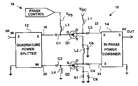
Referring now to FIGURE 10, a power-shifting rf amplifier, or power-
switching rf amplifier, 70 includes a splitting rf amplifier 72 and a power
control
74. The splitting rf amplifier 72 includes the quadrature power splitter 12,
the
FETs Q1 and Q2, the coupling capacitors C1, C2, C3, and C4, the decoupling
CA 02420710 2003-03-03
22
capacitors C5 and C6, the rf chokes L1, L2, L3, and L4, the resistor R1, and
rf
outputs RFi our and RF2~uT.
The power-shifting amplifier 70 proportions its rf output between the rf
outputs RF1 ouT and RF2our. or shifts the total rf output between the rf
outputs
RF1«uT and RF2ouT, in response to a power-shifting voltage VP~,,~, and in
accordance with both a magnitude of the power-shifting voltage VPwK and a rate
of
change thereof. The power-shifting voltage VPWR is generated, or supplied, by
the
power control 74. The power-shitting voltage VPWR, as applied to the gate
terminal
of the FET Q1, is effective to control gains of both FETs Q1 and Q2 as
described in
conjunction with FIGURE 1.
By varying the power-shifting voltage VP~NK both rapidly and with a
sufficient change in voltage, the rf output power can be switched almost
instantaneously from one of the rf outputs, RFI~u-, or RF2ou.r to the other
one of
the rf outputs, RF2ouT or RF1 ouT.
Both the phase control 16 of FIGURE 1 and the power control 74 of
FIGURE 10 represent any means for providing selectively-variable gate
voltages.
While the phase control 16 and the power control 74 vary in function, they do
not
necessarily vary in construction. That is, the phase control 16 provides a
phase-
shifting voltage for controlling a phase angle of the rf output RFouT of
FIGURE 1,
whereas the power control 74 of FIGURE 10 provides a power-shifting voltage
for
selectively and progressively shifting rf output power from the rf output
RF1our to
the rf output RF2ouT.
Even as the phase-shifting rf amplifier 10 of FIGURE 1 maintains
substantially constant rf power during phase shifting, the power-shifting rf
amplifier
70 of FIGURE 10 maintains a total rf output of the two rf outputs, RFlour and
RF2ouT, substantially constant whether the rf output is progressively shifted
or
switched almost instantaneously.
Since the rf input signal, RF,N, has been split by the quadrature power
splitter 12, quadrature rf signals are supplied to the gate terminals of the
FETs Q1
and Q2, and the rf outputs RF1 ~,uT and RF2~uT are in quadrature. But, if an
in-
phase splitter, similar to that shown in FIGURE 15, is substituted for the
quadrature
splitter 12, the two rf outputs RF1 our and RF2~,uT will be in phase.
CA 02420710 2004-10-O1
70828-29
23
Referring now to FIGURES 11 and 12, a variable power-shifting rf
amplifier, or power-switching amplifier, 80 includes both a splitting rf
amplifier 82
of FIGURE 11 and a power control 84 of FIGURE 12. In addition to components
named and numbered in conjunction with FIGURE 10, the splitting rf amplifier
82
includes the 180 degree spiitter 36, the 90 degree splitter 38A, the FET Q3,
the
capacitors C7, C8, and C9, and the rf chokes L5 and L6 of FIGURE 2.
The variable power-shifting rf amplifier 80 produces three rf outputs,
RF1ouT, RF2ouT, and RF3ouT. The power-shifting rf amplifier 80 will
selectively
shift, or abruptly switch, power between/among the rf outputs RF1 our, RF2ouT,
and
RF3ouT in response to power-shifting voltages VPWR, and VPW,~.
The power control 84 produces the power-shifting voltages VpWR, and
VPWRZ in response to an analog or digital input 86. As can be understood by
considering the discussion of FIGURE 2, the rf output RF2our, of the variable
power-shifting rf amplifier 80, is at 90.0 degrees to the rf output RF1 ouT,
and the rf
output RF3ouT is at 180 degrees to the rf output RF1 our.
The power control 84 is representative of any device that will produce the
power-shifting voltages VPWR, and VPW~ in response to the analog or digital
input
86, vary them in whatever manner is useful for a particular application, and
vary
them in whatever time frame may be desirable or suitable for an intended use
of
the power-shifting rf amplifier 80.
In the phase-shifting rf amplifier 30 of FIGURE 2, gains of the FETs Q1,
Q2, and Q3 are selectively varied by varying the phase-shifting voltages VPs,
and
VPSZ to the gates of the FETs Q1 and Q2, and the rf output RFouT is phase
shifted.
In like manner, in the power-shifting rf amplifier 80 of FIGURE 11, gains of
the FETs Q1, Q2, and Q3 are selectively varied by varying voltages applied to
gates of the FETs Q1 and Q2. However, in the power-shifting rf amplifier 80 of
FIGURE 11, the gate voltages are called power-shifting voltages VPWR, and
V~,~,RZ,
because these voltages selectively shift, or switch, the rf output among rf
outputs
RF1 ouT, RF2ouT, and RF3ouT.
Referring now to FIGURES 13 and 14, a variable power-shifting rf
amplifier, or power-switching amplifier, 90 includes both a splitting rf
amplifier 92
of FIGURE 13 and a power control 94 of FIGURE 14. In addition to components
named and numbered in conjunction with FIGURE 11, the splitting rf amplifier
92
CA 02420710 2004-10-O1
70828-29
24
of FIGURE 13 includes the 90 degree splitter 38B, the FET Q4, capacitors C10,
C11, and C12, and rf chokes L7 and L8.
The variable power-shifting rf amplifier 90 has four rf outputs, RFlour,
RF2our, RF3our, and RF4our. The power-shifting rf amplifier 90 will
selectively and
progressively shift, or abruptly switch, power between/among the rf power
outputs
RF1 our. RF2our~ RF3ouT~ and RF4our in response to power-shifting voltages
VpWR~,
VPWR2i and VpWR3'
The power control 94 produces the power-shifting voltages VPwR" VPW,~,
and VPWR3 in response to an analog or digital input 96. The rf output RF2our
is at
90.0 degrees to the rf output RFlour, the rf output RF3our is at 180 degrees
to the
rf output RFIouT, and the rf output RF4our is at 270 degrees to the rf output
RFlour.
The power control 94 is representative of any device that will produce the
power-shifting voltages VPWR" VPW~, and VPWR3 in response to the analog or
digital
input 96, vary them in whatever manner is useful for a particular application,
and
vary them in whatever time frame may be desirable or suitable for an intended
use
of the power-shifting rf amplifier 90.
Gains of the FETs Q1, Q2, Q3, and Q4 are selectively varied by varying
the power-shifting voltages VPWR" VPWR2, and VPWR3 to the gates of the FETs
Q1,
Q2, and Q3. As the power-shifting voltages VPWR,, VPWR2, and VPwR3 are
selectively
varied, the rf output is selectively shifted/proportioned among rf outputs
RF1our,
RF2our, RF3our, and RF4our.
Referring now to FIGURES 15 and 14, a variable power-shifting rf
amplifier, or power-switching amplifier, 100 includes both a splitting rf
amplifier
102 of FIGURE 15 and the power control 94 of FIGURE 14. However, the
splitting rf amplifier 102 includes parts generally as named and numbered in
conjunction with FIGURE 13. Instead of the power splitters 36, 38A, and 38B of
FIGURE 13, the splitting rf amplifier 102 includes an in-phase rf power
splitter 104
that produces four, in-phase rf signals.
As with the variable power-shifting rf amplifier 90 of FIGURE 13, the
variable power-shifting rf amplifier 100 of FIGURE 15 produces four rf
outputs,
CA 02420710 2004-10-O1
70828-29
24A
RFlour, RF2our, RF3our, and RF4our~ The power-shifting rf amplifier 100
will selectively shift, or abruptly switch, power between/among the rf outputs
RF1 our,
CA 02420710 2003-03-03
RF2~uT, RF3our, and RF4our in response to power-shifting voltages power VPWR1~
VPWKZ, and V,,W~3 that are generated by the power control 94 in response to
the
analog or digital input 96 of FIGURE 14.
Referring now to FIGURE 16 an antenna, or stub, 110A is mounted to a
5 top 1 12 of a fuselage 114 of an airplane 1 16; and an antenna, or stub, 1
10B is
mounted to a belly 118 of the fuselage 114. By attaching the rf outputs RFlour
and RF2~uT of the power-shifting rf amplifier 70 to respective ones of the
antennas,
110A and 1 10B, rf power may be selectively shifted, or switched, between the
antennas 1 10A and 110B to maintain optirnum ground link.
10 Referring now to FIGURE 17, an antenna array 120 includes antennas
122A, 122B, 122C, and 122D. By attaching one of the rf outputs, RF1 our,
RF2our~
RF3our, and RF4our of the power-shifting rf amplifier 100 to each of the
antennas,
122A, 122B, 122C, and 122D, and then selectively shifting the rf outputs RF1
our,
RF2our, RF3our, and RF4our, a radiation pattern, not shown, can be selectively
15 adjusted. Alternately, if the power-shifting rf amplifier 90 is used, phase
angles of
the rf outputs RF1 our, RF2our, RF3our, and RF4~uT can be applied to selective
ones
of the antennas 122A, 122B, 122C, and 122D to generate a variety of
additional,
new, and useful radiation patterns.
The ability of the power-shifting rf amplifiers 70, 80, 90, and 100 to
20 variably and progressively shift power from one rf output to an other, and
optionally to selectively switch rf power from one rf output to an other, has
various
applications.
For instance, the present invention provides a solid-state switch for
directing rf power from one rf power amplifier to an other, thereby providing
for
25 hot-switching of rf power from one rf power amplifier to an other when one
rf
power amplifier malfunctions.
As taught in conjunction with FIGURE 16, the present invention may be
used to variably shift rf output between/among antennas mounted on an
airplane,
to maintain optimal ground link.
As taught in conjunction with FIGURE 17, the present invention may be
used in antenna arrays, using selectively variable rf power to a plurality of
rf
outputs, such as the rf outputs RF1 «uT, RF2~uT, RF3«ur, and RF4our of FIGURES
13
and 15, to provide new and useful radiation patterns with, or without the
CA 02420710 2003-03-03
z6
additional variation provided by the quadrature rf outputs of the variable
power-
shifting rf amplifier 90 of FIGURE 13.
While the preceding discussion has focused on the use of FETs, bipolar
silicon transistors, and other solid-state amplifying devices may be used.
However,
FETs are preferred because of their high gain, thereby reducing the total
number of
amplification stages that are required to achieve the desired rf power output.
Therefore, it should be understood that the principles taught herein may be
applied
to other types of solid-state amplifying devices.
In summary, the present invention can be characterized as phase splitting
an rf input into a plurality of rf signals that are at either in phase or that
are at
different phase angles, selectively amplifying selected ones of the rf
signals,
producing a plurality of rf outputs that are either in phase or in quadrature,
and
that are at different rf power levels, and progressively shifting, or rapidly
switching,
rf power between/among the rf outputs.
The present invention can be characterized as applying a do voltage across
two or more FETs that are connected in series, and selectively utilizing all
of the
do voltage in one of the FETs, or dividing the do voltage between/among the
FETs.
The present invention can be characterized as power-shifting rf outputs
between/among a plurality of rf outputs without a total rf output decreasing
to
zero, or even changing appreciably.
Finally, the present invention can be characterized as providing optimum
rf decoupling, especially by reducing the effective series resistance (ESR) of
decoupling capacitors, thereby removing power limitations from rf power
amplifiers in which solid-state amplifying devices, such as FETs, are
connected in
series between a source-voltage and a lower-voltage.
While specific apparatus and method have been disclosed in the preceding
description, it should be understood thal these specifics have been given for
the
purpose of disclosing the principles of the present invention, and that many
variations thereof will become apparent to those who are versed in the art.
Therefore, the scope of the present invention is to be determined by claims
included herein without any limitation by numbers that may be parenthetically
inserted in the claims.
CA 02420710 2003-03-03
27
Industrial Applicability
The present invention provides rf power amplifiers, including rf amplifiers
in the gigahertz range, that selectively proportion, or rapidly switch, a
total rf
output between/among two or more outputs, whereby the total rf output can be
selectively proportioned, or rapidly switched between/among a plurality of
antennas m an array.