Note: Descriptions are shown in the official language in which they were submitted.
CA 02420941 2003-02-27
Amendment Page 1
6. Contents of Amendment
(1) Specification
In correspondence to the amendment on the claims
described below,
(1.1) the passage from "the light passes through the
light absorption layer 4" in Japanese text of line 1 on
page 16 (corresponding to the English translation page 18,
line 18) to "a sixth aspect of the present invention, there
is" in Japanese text of line 25 on page 17 (corresponding
to the English translation page 21, line 22) was cancelled
and an amendment was made as described in the attached
corresponding pages (Japanese amended text page 16 to
page 17/1) (corresponding to the amended English
translation pages 18 to 21);
(1.2) the passage from "at least one of a position
and an inclination when an" in Japanese text of line 1 on
page 20 (corresponding to the English translation page 24,
line 19) to "layer is 90°" in Japanese text of line 25 on
page 21 (corresponding to the English translation page 27,
line 11) was cancelled and an amendment was made as
described in the attached corresponding pages (Japanese
amended text page 20 to page 21/1) (corresponding to the
amended English translation pages 24 to 27/1);
(1.3) the passage from "FIG. 19 is a diagram for
explaining operations" in Japanese text of line 1 on
page 25 (corresponding to the English translation page 31,
line 20) to "is obtained" in Japanese text of line 25 on
CA 02420941 2003-02-27
Amendment Page 2
page 25 (corresponding to the English translation page 32,
line 21) was cancelled and an amendment was made as
described in the attached corresponding pages (Japanese
amended text page 25 and page 25/1) (corresponding to the
amended English translation pages 31 and 32);
(1.4) the passage from "made incident into both the
lower cladding layer 13 and" in Japanese text of line 1 on
page 34 (corresponding to the English translation page 43,
line 4) to "instead of the optical fiber 11" in Japanese
text of line 25 on page 34 (corresponding to the English
translation page 44) was cancelled and an amendment was
made as described in the attached corresponding pages
(Japanese amended text page 34 to page 34/1) (corresponding
to the amended English translation page );
(1.5) the passage from "type electrode 1 and the
p+-InGaAs contact layer 2 so" in Japanese text of line 1 on
page 45 (corresponding to the English translation page 57,
line 15) to "plane" in Japanese text of line 25 on page 45
(corresponding to the English translation page 58, line 26)
was cancelled and an amendment was made as described in the
attached corresponding pages (Japanese amended text page 45
to page 45/1) (corresponding to the amended English
translation pages 57 and 58).
Therefore, please substitute these amended pages for
the corresponding pages submitted at a time of filing
international application under PCT.
CA 02420941 2003-02-27
Amendment Page 3
(2) Claims
Claims l, 16 and 17 were amended.
The remaining claims 2 to 15 and 18 to 24 remains in
this application as they are.
Please substitute Japanese amended text pages 48 to
48/1 and pages 51 to 52/1 (corresponding to the amended
English translation page 61, 61/1, 62 and pages 65, 66,
66/1, 67, 67/l, 68) including this amendment for the
corresponding pages submitted at the time of filing the
international application.
Incidentally, the contents of amendment on claims are
as described in the following items (2.1) to (2.9), and the
contents of amendment are the underlined parts.
(2.1) The description "a lower cladding layer
laminated on an upper portion of the substrate and
constituted of at least one layer" in Japanese text of
lines 3 and 4 on page 48 (corresponding to the English
translation page 61, lines 4-6) in claim 1 was amended to a
description "a lower cladding layer which has a
predetermined refractive index, is laminated on an upper
portion of the substrate, and is constituted of at least
one layer".
(2.2) The description "an upper cladding layer
laminated above the light absorption layer and constituted
of at least one layer" in Japanese text of lines 6 to 7 on
page 48 (corresponding to the English translation page 61,
lines 9 to 11) in claim 1 was amended to a description "an
CA 02420941 2003-02-27
Amendment Page 4
upper cladding layer which has a refractive index smaller
than a refractive index of at least one layer constituting
the lower cladding layer, is laminated above the light
absorption layer, and is constituted of at least one
layer".
Incidentally, the ground of the amendment about the
above items (2.1) and (2.2) will be apparent from the
description "A material having a higher refractive index
than the lower cladding layer 3 made of p-InP (refractive
index n3 = 3.17), for example, a material of quaternary
composition having a band gap wavelength of 1.3 ~,m
(refractive index n13 = 3.39) is employed for the lower
cladding layer 13 made of n-InGaAsP" in Japanese text of
lines 16 to 20 on page 29 (corresponding to the English
translation page 37, lines 7-12) of the specification
submitted at the time of filing the international
application and the description "Also in the semiconductor
light receiving device according to the second embodiment,
the refractive index n13 of the lower cladding layer 13
made of n-InGaAsP into which the light is made incident is
set to be higher than the refractive index n3 of the upper
cladding layer 3 made of p-InP positioned at the upper side
of the light absorption layer 4" in Japanese text of
lines 19-23 on page 33 (corresponding to the English
translation page 42, lines 21-27).
(2.3) The description "a light incident end surface
which is provided on at least one of the substrate and the
CA 02420941 2003-02-27
Amendment Page 5
lower cladding layer, and, when a light is made incident at
a predetermined angle, enables the light to be absorbed in
the light absorption layer and to be output as a current"
in Japanese text of lines 8 to 11 on page 48 (corresponding
to the English translation page 61, lines 13-18) in claim 1
was amended to a description "a light incident end surface
which is provided at both the substrate and the lower
cladding layer, and, when a light is made incident at a
predetermined angle, enables the light to be absorbed in
the light absorption layer and to be output as a current".
Note that, the grounds for the amendment regarding
the above item (2.3) will be apparent from the description
"Here, it is desirable that the light is made incident on
the lower cladding layer 13 having the higher refractive
index, but even when the light is made incident on both the
lower cladding layer 13 and the substrate 9 in order that
the equivalent refractive index for the light is set to be
higher than the refractive index of the upper cladding
layer 3, the present invention can be accomplished" in
Japanese text of line 24 on page 33 to line 3 on page 34
(corresponding to the English translation page 43,
lines 1-8) of the specification submitted at the time of
filing the international application.
(2.4) The description "wherein an equivalent
refractive index of at least one of the substrate and the
lower cladding layer providing the light incident end
surface is higher than a refractive index of said at least
CA 02420941 2003-02-27
Amendment Page 6
one layer constituting the upper cladding layer, and
the predetermined angle enables a light incident on
the light absorption layer to be reflected at a lower
surface of said at least one layer constituting the upper
cladding layer" in Japanese text of lines 12 to 17 on
page 48 (corresponding to the English translation page 61,
lines 19-27) in claim 1 was amended to a description
"wherein the light incident on both the substrate and the
lower cladding layer providing the light incident end
surface senses a refractive index of the lower cladding
layer so that an equivalent refractive index of the light
becomes larger, and the equivalent refractive index of the
light becomes larger than a refractive index of said at
least one layer constituting the upper cladding layer
having a refractive index smaller than a refractive index
of said at least one layer constituting the lower cladding
la er, and
the predetermined angle is an angle enabling a light
incident into the light absorption layer to be reflected at
a lower surface of said at least one layer constituting the
upper cladding layer,
so that the light can be repeatedly propagated
through the light absorption layer".
Incidentally, the ground of the amendment about the
above item (2.4) will be apparent from the description "As
the rounded-end fiber is moved upward along the light
incident end surface 10 from the substrate 9 side, when the
CA 02420941 2003-02-27
Amendment Page 7
light emitted from the rounded-end fiber starts to sense
the high refractive index of the lower cladding layer 13
made of n-InGaAsP in addition to the substrate 9 shown in
FIG. 3, the equivalent refractive index of the incident
light becomes higher.
As a result, the equivalent refractive index of the
incident light becomes higher than the refractive index n3
of the upper cladding layer 3 made of p-InP positioned
above the light absorption layer 4, and the light is
reflected at the boundary between the light absorption
layer 4 made of i-InGaAs and the upper cladding layer 3
made of p-InP, and thereby the efficiency can be remarkably
improved" in Japanese text of lines 11 to 20 on page 45
(corresponding to the English translation page 58,
lines 5-19) of the specification submitted at the time of
filing the international application and the description
"The present invention is made in view of the above
circumstances, and it is an object of the present invention
to provide a semiconductor light receiving device in which
refractive indexes of a lower cladding layer and an upper
cladding layer are adjusted so that a light incident on a
light absorption layer can be propagated repeatedly though
the light absorption layer and a conversion efficiency of
the light incident from the light absorption layer into an
electric signal and the frequency response characteristics
can be remarkably improved, and a method of manufacturing
the same" in Japanese text of lines 4 to 10 on page 16
CA 02420941 2003-02-27
Amendment Page 8
(corresponding to the English translation page 18, line 24
to page 19, line 8).
(2.5) The description "a light incident end surface
formed on an end surface of at least one of the substrate
and the lower cladding layer" in Japanese text of lines 4
and 5 on page 51 (corresponding to the English translation
page 65, lines 19-21) in claim 16 was amended to a
description "a light incident end surface formed on both
end surfaces of the substrate and the lower cladding
layer".
(2.6) The description "laminating a lower cladding
layer constituted of at least one layer on an upper portion
of the substrate" in Japanese text of lines 18 and 19 on
page 51 (corresponding to the English translation page 66,
lines 17-19) in claim 17 was amended to a description
"laminating a lower cladding layer having a predetermined
refractive index and constituted of at least one layer on
an upper portion of the substrate".
(2.7) The description "laminating an upper cladding
layer constituted of at least one layer above the light
absorption layer" in Japanese text of lines 21 and 22 on
page 51 (corresponding to the English translation page 66,
lines 22 and 23) in claim 17 was amended to a description
"laminating an upper cladding layer having a refractive
index smaller than a refractive index of at least one layer
constituting the lower cladding layer and constituted of at
least one layer above the light absorption layer".
CA 02420941 2003-02-27
Amendment Page 9
(2.8) The description "making a light incident at a
predetermined angle onto at least one of the substrate and
the lower cladding layer to provide a light incident end
surface which enables the light to be absorbed in the light
absorption layer and to be output as a current" in Japanese
text of line 23 on page 51 to line 1 on page 52
(corresponding to the English translation page 66, line 25
to page 67, line 2) to line 1 on page 52 in claim 17 was
amended to a description "making a light incident onto both
the substrate and the lower cladding layer at a
predetermined angle to provide a light incident end surface
which enables the light to be absorbed in the light
absorption layer and to be output as a current".
(2.9) The description "wherein an equivalent
refractive index of at least one of the substrate and the
lower cladding layer providing the light incident end
surface is larger than a refractive index of said at least
one layer constituting the upper cladding layer, and
the predetermined angle is an angle enabling a light
incident into the light absorption layer to be reflected at
a lower surface of said at least one layer constituting the
upper cladding layer" in Japanese text of lines 2 to 7 on
page 52 (corresponding to the English translation page 67,
lines 3-11) in claim 17 was amended to a description
"wherein the light incident on both the substrate and the
lower cladding layer providing the light incident end
surface senses a refractive index of the lower cladding
CA 02420941 2003-02-27
Amendment Page 10
layer so that an equivalent refractive index of the light
becomes larger, and the equivalent refractive index of the
light becomes larger than a refractive index of said at
least one layer constituting the upper cladding layer
having a refractive index smaller than a refractive index
of said at least one layer constituting the lower cladding
layer, and
the predetermined angle is an angle enabling a light
incident into the light absorption layer to be reflected at
a lower surface of said at least one layer constituting the
upper cladding layer,
so that the light can be repeatedly propagated
through the light absorption layer".
Note that, the grounds for amendment regarding items
(2.5) to (2.9) correspond to the grounds for amendment
regarding items (2.1) to (2.4).
(3) Drawings
An attached FIG. 20 was added along the disclosure in
the passage "Here, it is desirable that the light is made
incident onto the lower cladding layer 13 having the higher
refractive index, but even when the light is made incident
onto both the lower cladding layer 13 and the substrate 9
in order that the equivalent refractive index for the light
is set to be higher than the refractive index of the upper
cladding layer 3, the present invention can be
accomplished" in Japanese text of line 24 on page 33 to
CA 02420941 2003-02-27
Amendment Page 11
line 3 on page 44 (corresponding to the English translation
page 43, lines 1-8) in the application at the time of
filling the international application.
As amendment was made in the above manner, please
examine this application according to a demand for
international preliminary examination of this international
application along the amended contents of the application.
Incidentally, as apparent from the grounds for
amendment, we believe that the contents of amendment of the
present application do not exceed the scope of the
invention disclosed at the time of filing this
international application.
7. List of Documents Attached
(1) Corresponding amended pages (Japanese amended
pages 16 to 17/1), (pages 20 to 21/1), (pages 25 to 25/1),
(pages 34 to 34/1) and (pages 45 to 45/1) (corresponding to
the amended English translation pages 18, 19, 19/1, 20,
20/1, 21, 24, 25, 26, 26/1, 27, 27/1, 31, 31/1, 32, 43,
43/1, 44, 57, 57/1, 58)
(2) Corresponding pages of amended claims (Japanese
amended pages 48 to 48/1 and pages 51 to 52/1)
(corresponding to the amended English translation pages 61,
61/1, 62, 65, 66, 66/1, 67, 67/1, 68)
(3) Page 11/11 including added figure in the drawings
(FIG. 20)
CA 02420941 2003-02-27
18
p+-InGaAs so that ohmic contact can be obtained.
At this time, the metal components described above
enter the inside of the contact layer 2 made of
p+-InGaAs, and thereby the crystallinity of the contact
layer 2 is deteriorated and the smoothness of the
interface between the p electrode 1 and the contact
layer 2 made of p+-InGaAs is remarkably deteriorated.
Therefore, when the light reaches these areas,
many carriers which do not contribute to the
photoelectric conversion by the contact layer 2 made of
p+-InGaAs occur and the scattering loss of the light is
also large, and consequently the efficiency of the
photoelectric conversion and the frequency response
characteristics as the semiconductor light receiving
device are deteriorated.
In this manner, in the conventional semiconductor
light receiving devices shown in FIG. 14 and FIG. 18,
the light passes through the light absorption layer 4
according to Snell's law in geometrical optics so that
there are the problems that the conversion efficiency
of the light into the electric signal is low and the
frequency response characteristics are deteriorated.
Disclosure of Invention
The present invention is made in view of the above
circumstances, and it is an object of the present
invention to provide a semiconductor light receiving
device in which refractive indexes of a lower cladding
CA 02420941 2003-02-27
19
layer and an upper cladding layer are adjusted so that
a light incident on a light absorption layer can be
propagated repeatedly though the light absorption layer
and a conversion efficiency of the light incident from
the light absorption layer into an electric signal and
the frequency response characteristics can be
remarkably improved, and a method of manufacturing the
same.
In order to achieve the above object, according to
a first aspect of the present invention, there is
provided a semiconductor light receiving device
comprising:
a substrate (9);
a lower cladding layer (13) which has a predeter-
mined refractive index, is laminated on an upper
portion of the substrate, and is constituted of at
least one layer;
a light absorption layer (4) laminated on an upper
portion of the lower cladding layer;
an upper cladding layer (3) which has a refractive
index smaller than a refractive index of said at least
one layer constituting the lower cladding layer, is
laminated above the light absorption layer, and is
constituted of at least one layer; and
a light incident end surface (10) which is
provided at both the substrate and the lower cladding
layer, and, when a light is made incident at a
CA 02420941 2003-02-27
19/1
predetermined angle, enables the light to be absorbed
in the light absorption layer and to be output as a
current,
CA 02420941 2003-02-27
wherein the light incident on both the substrate
and the lower cladding layer providing the light
incident end surface senses a refractive index of the
lower cladding layer so that an equivalent refractive
5 index of the light becomes larger, and the equivalent
refractive index of the light becomes larger than a
refractive index of said at least one layer
constituting the upper cladding layer having a
refractive index smaller than a refractive index of
10 said at least one layer constituting the lower cladding
layer, and
the predetermined angle is an angle enabling a
light incident on the light absorption layer to be
reflected at a lower surface of at least one layer
15 constituting the upper cladding layer,
so that the light can be repeatedly propagated
through the light absorption layer.
In order to achieve the above object, according to
a second aspect of the present invention, there is
20 provided a semiconductor light receiving device
according to the first aspect,
wherein, after the light is obliquely incident on
the light incident end surface and is further obliquely
incident on the light absorption layer to be
propagated,
the light is reflected at an interface of an upper
side of the light absorption layer or at an interface
CA 02420941 2003-02-27
20/1
of at least one layer constituting the upper cladding
layer positioned at an upper side of the light
absorption layer, and
the light propagates obliquely downward through
the light absorption layer again.
In order to achieve the above object, according to
a third aspect of the present invention, there is
provided a semiconductor light receiving device
according to the first aspect, wherein an angle formed
CA 02420941 2003-02-27
21
by the light incident end surface and a lower surface
of the light absorption layer is 90°.
In order to achieve the above object, according to
a fourth aspect of the present invention, there is
provided a semiconductor light receiving device
according to the first aspect, wherein an angle formed
by the light incident end surface and an lower surface
of the light absorption layer is less than 90°, and is
greater than an angle defined by a crystal orientation
of a material constituting the light incident end
surface.
In order to achieve the above object, according to
a fifth aspect of the present invention, there is
provided a semiconductor light receiving device
according to the first aspect, wherein an angle formed
by the light incident end surface and a lower surface
of the light absorption layer is less than 90°, and
larger than an angle defined by a crystal orientation
of a material constituting the light incident end
surface.
In order to achieve the above object, according to
a sixth aspect of the present invention, there is
provided a semiconductor light receiving device
according to the first aspect, wherein the lower
cladding layer is made of a semiconductor material of
quaternary composition.
In order to achieve the above object, according to
CA 02420941 2003-02-27
24
make the light obliquely incident on the light incident
end surface, a casing (12) which holds the
semiconductor light receiving device inclined by a
wedge-shaped pedestal (14) arranged at a lower side of
the substrate is provided so that a light is made
obliquely incident on the light incident end surface
from an optical fiber (11).
In order to achieve the above object, according to
a fourteenth aspect of the present invention, there is
provided a semiconductor light receiving device
according to the second aspect, wherein, in order to
make the light obliquely incident on the light incident
end surface, a casing (12) which holds the
semiconductor light receiving device is provided, a
lens holder (16) having a lens (17) fixed therein is
provided in the casing, and a light is made obliquely
incident on the light incident end surface from an
optical fiber (11) contained in the lens holder so that
at least one of a position and an inclination when an
incident light is incident on the light incident end
surface can be adjusted.
In order to achieve the above object, according to
a fifteenth aspect of the present invention, there is
provided a semiconductor light receiving device
according to the fourteenth aspect, wherein the
semiconductor light receiving device is inclined by a
wedge-shaped pedestal (14) arranged at a lower side of
CA 02420941 2003-02-27
the substrate.
In order to achieve the above object, according to
a sixteenth aspect of the present invention, there is
provided a semiconductor light receiving device
5 comprising:
a substrate;
a lower cladding layer, a light absorption layer
and an upper cladding layer laminated on the substrate
in the order;
10 a light incident end surface formed on both end
surfaces of the substrate and the lower cladding layer;
and
a p electrode and an n electrode which output an
electric signal generated by the fact that a light
15 incident from the light incident end surface is
absorbed in the light absorption layer to the outside
via the upper cladding layer and the lower cladding
layer, respectively,
wherein, in order that, after the light incident
20 on the light incident end surface is refracted at the
light incident end surface and then is made obliquely
incident on the light absorption layer to be
propagated, the light is totally reflected at an
interface of an upper side of the light absorption
25 layer or at an interface of a semiconductor layer
positioned at an upper side of the light absorption
layer to be propagated obliquely downward through the
CA 02420941 2003-02-27
26
light absorption layer again,
a refractive index of the lower cladding layer is
set to be higher than a refractive index of the upper
cladding layer.
In order to achieve the above object, according to
a seventeenth aspect of the present invention, there is
provided a method of manufacturing a semiconductor
light receiving device, comprising:
providing a substrate (9);
laminating a lower cladding layer (13) having a
predetermined refractive index and constituted of at
least one layer on an upper portion of the substrate;
laminating a light absorption layer (4) on an
upper portion of the lower cladding layer;
laminating an upper cladding layer (3) having a
refractive index smaller than a refractive index of
said at least one layer constituting the lower cladding
layer and constituted of at least one layer above the
light absorption layer;
making a light incident onto both the substrate
and the lower cladding layer at a predetermined angle
to provide a light incident end surface (10) which
enables the light to be absorbed in the light
absorption layer and to be output as a current,
wherein the light incident on both the substrate
and the lower cladding layer providing the light
incident end surface senses a refractive index of the
CA 02420941 2003-02-27
26/1
lower cladding layer so that an equivalent refractive
index of the light becomes larger, and the equivalent
refractive index of the light becomes larger than a
refractive index of said at least one layer
constituting the upper cladding layer having a
refractive index smaller than a refractive index of
said at least one layer constituting the lower cladding
layer, and
CA 02420941 2003-02-27
27
the predetermined angle is an angle enabling a
light incident on the light absorption layer to be
reflected at a lower surface of said at least one layer
constituting the upper cladding layer,
so that the light can be repeatedly propagated
through the light absorption layer.
In order to achieve the above object, according to
an eighteenth aspect of the present invention, there is
provided a method of manufacturing a semiconductor
light receiving device according to the seventeenth
aspect, wherein an angle formed by the light incident
end surface and a lower surface of the light absorption
layer is 90°.
In order to achieve the above object, according to
a nineteenth aspect of the present invention, there is
provided a method of manufacturing a semiconductor
light receiving device according to the seventeenth
aspect, wherein an angle formed by the light incident
end surface and a lower surface of the light absorption
layer is less than 90°, and is greater than an angle
defined by a crystal orientation of a material
constituting the light incident end surface.
In order to achieve the above object, according to
a twentieth aspect of the present invention, there is
provided a method of manufacturing a semiconductor
light receiving device according to the seventeenth
aspect, wherein an angle formed by the light incident
CA 02420941 2003-02-27
27/1
end surface and a lower surface of the light absorption
layer is less than 90°, and larger than an angle
CA 02420941 2003-02-27
31
configuration of a conventional semiconductor light
receiving device;
FIG. 13 is a diagram for explaining a problem of
the conventional semiconductor light receiving device;
FIG. 14 is a transverse sectional view showing a
schematic configuration of another conventional
semiconductor light receiving device;
FIG. 15 is a diagram for explaining operations of
another conventional semiconductor light receiving
device;
FIG. 16 is a transverse sectional view showing a
schematic configuration of still another conventional
semiconductor light receiving device;
FIG. 17 is a transverse sectional view showing a
schematic configuration of still another conventional
semiconductor light receiving device;
FIG. 18 is a transverse sectional view showing a
schematic configuration of still another conventional
semiconductor light receiving device;
FIG. 19 is a diagram for explaining operations of
still another conventional semiconductor light
receiving device; and
FIG. 20 is a transverse sectional view showing a
schematic configuration of a semiconductor light
receiving device according to a modified example of the
second embodiment of the present invention.
CA 02420941 2003-02-27
31/1
Best Mode of Carrying Out the Invention
First, prior to describing respective embodiments
of the present invention, in order to derive basic
concepts of the present invention, problems of
refraction (that is, light passes through) and
CA 02420941 2003-02-27
32
reflection of a light in the case of a multilayered
film structure will be considered using geometrical
optics used for discussion in Jpn. Pat. Appln. KOKAI
Publication Nos. 11-195807 and 2000-243984 in which the
conventional semiconductor light receiving devices
shown in FIG. 14 and FIG. 18 are described.
Now, as shown in FIG. 1, a multilayered film made
of l, 2, 3, ... ... ..., k, k+1 kinds of media is considered.
If Snell's law is applied at boundaries between
the respective media 1, 2, 3, ... ... ..., k, k+1, at the
boundary between the medium 1 and the medium 2,
nlsinAl = n2sin82 (9)
is obtained.
At the boundary between the medium 2 and the
medium 3,
n2sin62 = n3sinA3 (10)
is obtained.
At the boundary between the medium 3 and the
medium 4,
n3sin93 = n4sin64 (11)
is obtained.
Hereinafter, in a similar manner, at the boundary
between the medium k-2 and the medium k-1,
nk_2sinAk_2 = nk_lsin6k_1 (12)
is obtained.
At the boundary between the medium k-1 and the
medium k,
CA 02420941 2003-02-27
43
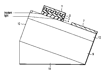
Here, it is desirable that the light is made
incident into the lower cladding layer 13 having the
higher refractive index, but even when the light is
made incident into both the lower cladding layer 13 and
the substrate 9 in order that the equivalent refractive
index for the light is set to be higher than the
refractive index of the upper cladding layer 3, the
present invention can be accomplished, as shown in
FIG. 20 as a modified example.
The actual measurement result of the semiconductor
light receiving device shown in FIG. 20 as the modified
example is as follows.
In the case of the semiconductor light receiving
device shown in FIG. 20 as the modified example, the
thickness of the lower cladding layer 13 can be made
thinner so that manufacture is facilitated.
The concept shown in FIG. 20 as the modified
example can be applied not only to the second
embodiment of the present invention but also to other
embodiments of the present invention including the
first embodiment.
In the semiconductor light receiving device
according to the second embodiment, the lower cladding
layer 5 made of n-InP is interposed between the light
absorption layer 4 made of i-InGaAs and the lower
cladding layer 13 made of n-InGaAsP.
Since, when the thickness of the lower cladding
CA 02420941 2003-02-27
43/1
layer 5 is as thin as about 1 dun, the influence on the
optical path is small, it is substantially possible to
remove the lower cladding layer 5.
Therefore, since the angle of incidence of light
entering the light absorption layer 4 is made smaller
and the light is
CA 02420941 2003-02-27
44
reflected at the interface between the upper cladding
layer 3 made of p-InP (refractive index n3) and the
light absorption layer 4, the inclination of the light
propagating through the light absorption layer 4 is
smaller as compared with the conventional semiconductor
light receiving devices also in the present embodiment
so that the effective absorption length of the light
can be made longer.
Furthermore, also in the present embodiment, since
the light is reflected at the interface, the effective
absorption length is multiplied so that the efficiency
as the semiconductor light receiving device can be
remarkably improved.
In addition, in the present embodiment, it goes
without saying that the light may be made incident
obliquely from below using a lens system instead of the
optical fiber 11.
(Third embodiment)
FIG. 5 is a transverse sectional view showing a
schematic configuration of a semiconductor light
receiving device according to a third embodiment of the
present invention.
In FIG. 5, like reference numerals are denoted to
like parts identical to those of the semiconductor
light receiving device according to the second
embodiment shown in FIG. 4, and detailed description of
the overlapping parts will be omitted.
CA 02420941 2003-02-27
57
In the description so far, it is assumed that the
lower cladding layer 13 is entirely doped into the same
type, but only part thereof need be doped.
Moreover, for alloying when the ohmic contact is
realized, the contact layer 2 made of p+-InGaAs is
deteriorated in the crystallinity and the smoothness of
the interface between the p type electrode 1 and the
contact layer 2 made of p+-InGaAs is remarkably
deteriorated.
However, in the present invention, the light
propagating obliquely upward from the lower side is
reflected obliquely downward at the interface of the
semiconductor layers, the light is not easy to be
influenced by the p+-InGaAs contact layer 2, or the p
type electrode 1 and the p+-InGaAs contact layer 2 so
that the efficiency of the photoelectric conversion and
the frequency response characteristics are remarkably
good.
Here, the actual measurement result of the
semiconductor light receiving device according to the
first embodiment of the present invention shown in
FIG. 2 will be described with reference to FIG. 10.
In addition, this actual measurement result can
similarly be applied to all other embodiments including
the modified example in FIG. 20.
In other words, FIG. 10 shows measurement values
of a photocurrent obtained when the rounded-end fiber
CA 02420941 2003-02-27
57/1
is moved upward from the substrate 9 side along the
light incident end surface 10 in the case where the
inclination 61 of the incident light is 35° (the
CA 02420941 2003-02-27
58
incident light is directed from obliquely lower left to
obliquely upper right as shown in FIG. 3).
In this case, the power of the input light is
-8.1 dBm.
As the rounded-end fiber is moved upward along the
light incident end surface 10 from the substrate 9
side, when the light emitted from the rounded-end fiber
starts to sense the high refractive index of the lower
cladding layer 13 made of n-InGaAsP in addition to the
substrate 9 shown in FIG. 3 (FIG. 20), the equivalent
refractive index of the incident light becomes higher.
As a result, the equivalent refractive index of
the incident light becomes higher than the refractive
index n3 of the upper cladding layer 3 made of p-InP
positioned above the light absorption layer 4, and the
light is reflected at the boundary between the light
absorption layer 4 made of i-InGaAs and the upper
cladding layer 3 made of p-InP, and thereby the
efficiency can be remarkably improved.
Here, the thickness of the light absorption layer
4 is 0.4 ~,m.
Note that, in this experiment, the end surfaces of
the light absorption layer 4, the upper cladding layer
3, and the contact layer 2 and the light incident end
surface 10 employ the device positioned on the same
plane.
That is to say, in this device, the distance. from