Note: Descriptions are shown in the official language in which they were submitted.
CA 02421896 2003-03-13
-1-
A SWITCH MODEL COMPONENT
FIELD OF THE INVENTION
The present invention relates to switching apparatus. In
particular, the invention relates to an apparatus for
modelling a plurality of switching operations.
BACKGROUND TO THE INVENTION
An important parameter by which telecommunications
apparatus are measured is the ability to restore traffic
quickly in the event of a fault. This is normally
achieved by protection switching. A protection switch is
arranged to select one of, typically, two available
inputs. When an input is selected, the traffic received
on that input is passed on by the protection switch. When
a fault is detected in respect of the selected input, the
protection switch selects the other available input.
Moreover, it is common for telecommunications apparatus to
comprise more than one layer of protection switching. As
a result, the connections between respective inputs and
outputs of a telecommunications apparatus may depend on
the respective settings of more than one protection
switch.
Telecommunications apparatus is becoming increasingly
complicated and are typically required to handle a very
large number, typically thousands, of input and output
traffic data signals. Accordingly, a typical
CA 02421896 2003-03-13
-2-
telecommunications apparatus may be required to implement
thousands of protection switches. The respective settings
of these protection switches must be determined before the
connections between the inputs and outputs of the
telecommunications apparatus can be configured.
A problem here is that, in order to conform with industry
standards such as ITU-T (International Telecommunications
Union Telecommunications Standardization Sector) and
Telcordia standards and customer expectations, protection
switching must be performed within relatively strict time
limits. Moreover, these time limits are expected to be
met irrespective of the number of switching operations
that need to be implemented. It is thus becoming
increasingly difficult to perform the necessary switching
operations, determine the setting of the protection
switches and configure the connections between inputs and
outputs within the time limits stipulated by industry
standards.
This is a particular problem where it is desired to
implement the required switching operations in a single
core or microchip (sometimes referred to a single stage
switch or monolithic switch). In such a switch, all of
the necessary switching operations are performed in a
single stage normally under the control of computer
software. The computer software therefore tends to be
relatively complex and slow.
CA 02421896 2003-03-13
-3-
SUMMARY OF THE INVENTION
A first aspect of the invention provides an apparatus for
modelling a plurality of switching operations arranged in
a plurality of switching stages, the apparatus comprising
at least one respective switch stage component for each
switching stage, each switch stage component comprising
one or more respective addressable switch state indicators
for each switching operation associated with the
respective switching stage, wherein the value of the or
each switch state indicator in one or more of said switch
stage components identifies a respective switch state
indicator in another switch stage component and wherein
the switch stage components are interconnected such that
addressing a switch state indicator in one switch stage
component causes the respective identified switch state
indicator to be addressed.
In the preferred embodiment, the apparatus is associated
with a switch core having a plurality of inputs and a
plurality of outputs, the apparatus comprising a first
switch stage component and a final switch stage component,
wherein the respective switch state indicators of the
final switch state component correspond with a respective
output and the respective values of the switch state
indicators of said first switch stage component identify a
respective input.
The apparatus significantly reduces the time taken to
configure or reconfigure the switch core when protection
switching is required.
CA 02421896 2003-03-13
-4-
Preferably, the apparatus further comprises one or more
intermediate switch stage components between said first
and final switch stage components, wherein the respective
values of the switch state indicators of said one or more
intermediate switch stage components identify a respective
switch state indicator of a preceding intermediate switch
stage component or of said first switch stage component.
A second aspect of the invention provides a switching
apparatus comprising a switch core having a plurality of
inputs and a plurality of outputs, the apparatus further
comprising an apparatus for modelling a plurality of
switching operations according to the first aspect of the
invention.
A third aspect of the invention provides a network element
comprising a switching apparatus according to the second
aspect of the invention.
A fourth aspect of the invention provides a transport
network comprising one or more network elements according
to the third aspect of the invention.
A fifth aspect of the invention provides a method of
modelling a plurality of switching operations arranged in
a plurality of switching stages using an apparatus
comprising a respective switch stage component for each
switching stage, each switch stage component comprising a
respective addressable switch state indicator for each
switching operation associated with the respective
CA 02421896 2003-03-13
-5-
switching stage, the method comprising addressing a switch
state indicator it one of said switch stage components and
using the value of the addressed switch state indicator to
address a switch state indicator in another switch stage
component.
A sixth aspect of the invention provides a method of
protection switching using an apparatus for modelling a
plurality of switching operations arranged in a plurality
of switching stages comprising a respective switch stage
component for each. switching stage, each switch stage
component comprising a respective addressable switch state
indicator for each switching operation associated with the
respective switching stage, the method comprising
addressing a switch state indicator in one of said switch
stage components and using the value of the addressed
switch state indicator to address a switch state indicator
in another switch stage component.
A seventh aspect of the invention provides a computer
program product comprising computer useable instructions
for creating an apparatus according to the first aspect of
the invention. The computer program product may for
example take the form of hardware description language,
such as VHDL, or a netlist.
Preferred features of the invention are set out in the
dependent claims. Other advantageous aspects and features
of the invention will be apparent to those ordinarily
skilled in the art upon review of the following
CA 02421896 2003-03-13
-6-
description of a specific embodiment of the invention and
with reference to the accompanying drawings.
The preferred features as described herein above or as
described by the dependent claims filed herewith may be
combined as appropriate, and may be combined with any of
the aspects of the invention as described herein above or
by the independent claims filed herewith, as would be
apparent to those skilled in the art.
BRIEF DESCRIPTION OF THE DRAWINGS
Embodiments of the invention are now described by way of
example and with reference to the accompanying drawings in
which:
Figure 1 is a schematic view of a transport network;
Figures 2a and 2b show schematic views of a switching
apparatus;
Figure 3 is a schematic view of a switching apparatus
including an apparatus for modelling a plurality of
switching operations in accordance with a preferred
embodiment of the invention;
Figures 4a to 4c illustrate a first example operation of
the apparatus of Figure 3;
Figures 5a to Sc illustrate a second example operation of
the apparatus of Figure 3;
CA 02421896 2003-03-13
-7-
Figures 6a to 6c illustrate a third example operation of
the apparatus of Figure 3;
Figures 7a to 7c illustrate a fourth example operation of
the apparatus of Figure 3; and
Figure 8 shows a schematic view of an alternative
embodiment of a switching apparatus including an apparatus
for modelling a plurality of switching operations.
DETAILED DESCRIPTION OF THE DRAWINGS
Figure 1 of the drawings shows, generally indicated at 10,
a transport network comprising a plurality of network
elements 12 in communication with .one another via a
network infrastructure 14. The network infrastructure 14
may comprise further network elements or nodes, and/or
sub-networks, arranged in conventional network
configurations such as ring configuration, hub
configuration, mesh configuration, point-to-point
configuration, or a combination thereof. The network
elements 12 typically comprise telecommunications
apparatus, or transmission apparatus, such as a router, a
switch, a multiplexer, a regenerator or a cross-connect
(not shown), or a combination of these. The network 10
may, for example, comprise a synchronous transport
network, or synchronous transmission system, such as a
SONET and/or SDH network. In this case, the transmission
apparatus are commonly known as synchronous transmission
apparatus. Many synchronous transmission apparatus,
CA 02421896 2003-03-13
-8-
including multiplexers, routers and cross-connects,
comprise switching apparatus and the present invention may
best be described in the context of a switching apparatus.
Figure 2a shows a schematic view of a switching apparatus,
generally indicated at 20. The switching apparatus 20 may
form at least part of a synchronous transmission apparatus
(not shown) or network element 12. The switching
apparatus 20 comprises a switch device, or switch core 21,
for example a SONET STS (Synchronous Transport Signal)
switch (or equivalent high order switch), arranged to
receive a plurality of inputs 22 and provide a plurality
of outputs 24. It will be understood that the inputs 22
and outputs 24 do not necessarily correspond one-to-one
with physical input ports, output ports or input/output
(I/O) ports of the switching apparatus 20 or of the
synchronous transmission apparatus with which they are
associated. A physical input port, output port or I/O
port may send and/or receive data signals on one or more
inputs 22 and/or outputs 24, depending on the capacity of
the port and on the size of the data signal. In SDH and
SONET systems, the inputs 22 and outputs 24 are commonly
referred to as timeslots such that, for example, a
particular input 22 may correspond to a respective
timeslot on a particular port.
The main function of the switch core 21 is to cross-
connect the inputs 22 and outputs 24 so that traffic, or
data signals, arriving at a given input 22 are output from
the switch core 21 at one or more appropriate respective
outputs 24. The configuration of the switch core 21 is
CA 02421896 2003-03-13
-9-
determined by the contents of a table or connection map 52
which identifies which input 22 is connected to which
output 24. As shown in Figure 2a, the map 52 normally
resides in the switch core 21 and typically takes the form
of RAM (Random Access Memory) or other suitable memory.
Figure 2a shows the switch core 21 as a single stage
switch implemented as a single component, for example a
single microchip. Single component switches are sometimes
referred to as monolithic switches. The present invention
has particular relevance to single stage switches.
The switching apparatus 20 further includes a control
module 26. The control module 26 usually comprises
computer software embedded in a microcontroller or
microprocessor. The control module 26 is programmable to
configure the appropriate cross-connections between inputs
22 and outputs 24 and so to configure the switch core 21.
Typically this is achieved by way of assigning one or more
inputs to a respective one or more outputs. In order to
determine which input(s) need to be connected to which
output(s), the control module 26 needs to take into
account what protection switching, if any, the switching
apparatus 20 is required to make. Typically, this is
achieved with the assistance of an interface module 28.
The interface module 28 is arranged to, amongst other
things, examine or monitor each data signal received at
the inputs 22 and to communicate information relating to
the status of the data signals to the control module 26.
The status information comprises information relating to
faults detected in respect of the data signals received at
the inputs 22. For example, the status information may
CA 02421896 2003-03-13
-10-
indicate whether a respective data signal is non-faulty,
i.e. no protection switching is required in respect of the
signal, or faulty, i.e. protection switching is required
in respect of the signal. The evaluation of whether a
signal is faulty or non-faulty may be made on one or more
different parameters including level of bit error rate in
the signal (or other signal degradation), loss of signal
(usually indicated by an Alarm Indicator Signal (AIS)), or
signal mis-direction. The interface module 28 may
therefore be arranged to signal to the control module 26
either that a signal received on an input 22 is either
"faulty" or "non-faulty", and/or may provide other
parameters that allow the control module 26 to determine
whether or not it is necessary to perform a protection
switching operation (sometimes referred to as a protection
switching event). Examples of functions that may form
part of the interface module 28 are described in ITU-T
standards G.783 and G.806 in the context of SDH networks
and include the RSrn_TT, MSn_TT, Sn_TT, Sm__TT, Snm_TT,
Smm_TT, Sns_TT and Sms TT functions.
Once the control module 26 has received all of the
relevant status information from the interface module 28,
it determines what protection switching is required and
then configures the cross-connection between inputs 22 and
outputs 24 of the switch core 21 accordingly. However,
the switching apparatus 20 may receive thousands of data
signals at a time and may be required to implement more
than one protection switching scheme. As a result, the
amount of computation required by the control module 26 to
determine the appropriate switch configuration is
CA 02421896 2003-03-13
-11-
relatively high. It is increasingly difficult, therefore,
to devise a control module 26 which is able to configure
the switch core 21 quickly enough to meet the industry
standards laid down for protection switching (for example
ITU-T G.783 and G.841) as well as customer expectations.
Figure 2b shows a model of the switch core 21 and in
particular a model of the switching operations that the
switch core may be required to make. In Figure 2b it is
assumed, for illustration purposes only, that the
switching apparatus 20 is required to implement a section
protection switching scheme, such as BLSR (Bi-directional
Line Switched Ring, as specified in the Telcordia GR--1230-
CORE standard), and a path protection switching scheme,
such as UPSR (Unidirectional Path Switched Ring, as
specified for example in Telcordia GR-1400-CORE standard).
To implement the section protection switching, the
switching apparatus 20 is required to implement two or
more stages, or layers, of switching operations
represented in Figure 2b as two stages, namely stage 1 and
stage 3. To implement the path protection switching, the
switching apparatus is required to implement a further one
or more stage, or layer, of switching operations indicated
as one stage, namely stage 2. Each stage 1, 2 and 3
represents a respective set of protection switching
operations, or protection switches, that are required to
implement the respective protection switching schemes.
The switch core 21 does not normally comprise physical
switches corresponding to the switching operations, or
protection switches, of each stage 1 to 3. The protection
switches represented by stages 1, 2 and 3 may therefore be
CA 02421896 2003-03-13
-12-
considered as virtual switches and are implemented by the
programming of the control module 26 and the configuration
of the map 52. As is normal, the switch core 21 also
performs cross-connect operations corresponding to the
normal operation of the switching apparatus 20 i.e. the
switching that the switching apparatus 20 is required to
perform over and above any protection switching that is
required. In Figure 2b, the normal cross-connect
operations are represented by a fourth stage, or layer,
annotated as XCONN. It will be noted that the arrangement
of Figure 2b is provided by way of example only and that,
in practice the number and arrangement of switching stages
will depend on, amongst other things, the number and type
of protection switching schemes that the switching
apparatus 20 is required to implement.
In order to determine which inputs 22 must be connected to
which outputs 24 during any given period, the control
module 26 must determine the respective settings of the
protection switches, or virtual protection switches, in
each of stages 1, 2 and 3. Moreover, the control module
26 must take into account the respective setting of all of
the stages 1, 2 and 3 when determining how to connect an
input 22 to a given output 24. Thus, for each output 24,
the control module 26 traces a path back through a model
or map of each stage of the switch core 21 to determine
the, or each, appropriate input 22. The configuration of
the XCONN stage may be assumed to be constant for the
purposes of the present illustration, although this
configuration is changeable - typically at the behest of a
(human) network operator (not shown) via the control
CA 02421896 2003-03-13
-13-
module 26 - if it is desired to change the normal
switching operations performed by the switch core 21 (this
is sometimes known as a "connection time event" whereas
the protection switching operations are sometimes known as
"protection time events").
Conventionally, the control module 26 is programmed with a
model of the stage 1, 2 and 3 protection switches and with
the protection switching schemes that require
implementation. Upon receipt of the relevant data signal
status information from the interface module 28, the
control module 26 determines the appropriate configuration
for cross-connecting the inputs 22 and outputs 24. This
is a computationally intensive task which can take a
relatively long time to perform.
The present invention reduces the amount of time taken to
determine the appropriate configuration of the switch core
21, and in particular reduces the time taken to implement
protection time events, as is now described.
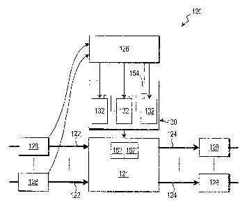
Figure 3 shows a schematic view of a switching apparatus,
generally indicated at 120, arranged in accordance with a
preferred embodiment of the present invention. The
switching device 120 comprises a switch core 121 having a
plurality of inputs 122 and a plurality of outputs 124
(only two of each shown), the switch core 121 being
substantially similar to the switch core 21 of Figure 2.
The switch core 121. includes, or has access to, a
connection map 152 the contents of which determines the
how the inputs 122 and outputs 124 are interconnected. In
CA 02421896 2003-03-13
-14-
Figure 3, a stand-by map 152' is also shown and is
described in more detail below. In the preferred
embodiment, the switch core 121 is particularly suited for
switching data signals comprising high order data
structures (for example, SDH VC-4s or SONET STS SPEs) and
comprises a high order switch, such as an STS switch, or
equivalent high order switch. It is also preferred that
the switch core 121 comprises a single stage switch. Also
shown in Figure 3 are interface modules 128, a respective
interface module 128 being associated with a respective
input 122. It will be noted that a single interface
module 128 may associated with one or more inputs 122 or
outputs 124. The switching apparatus 120 further includes
a control module 126 comprising, for example, computer
software embedded in a microprocessor or microcontroller.
As for the switching apparatus 120 of Figure 2a, the
interface modules 128 associated with inputs 122 are
arranged to communicate to the control module 126
information relating to the status of the traffic, or data
signals, received on the respective input 122.
In accordance with one aspect of the invention, the
switching apparatus 120 further includes an apparatus for
modelling a plurality of switching operations in the form
of a switch model component 130. The switch model
component 130 comprises a respective switch stage
component for one or more of the switching stages, or
layers, to be implemented by the switch core 121. In the
present example, it is assumed that the switching
apparatus 120 is required to implement three protection
switching stages, stages 1, 2 and 3, and one cross-
CA 02421896 2003-03-13
-15-
connection stage XCONN, as illustrated in Figure 2b. In
the preferred embodiment, the switch model component 130
is required to model only the protection switching stages
1, 2 and 3. Thus, the switch model component 130
comprises three switch stage components, namely a first
switch stage component 132, an intermediate switch stage
component 134, and a final switch stage component 136
corresponding to switching stages 1, 2 and 3 respectively.
For the purposes of clarity, in this example the
configuration of the XCONN stage is assumed to be constant
and the cross-connection stage XCONN is not represented in
the switch model component 130. In practice, the XCONN
stage may be implemented by one or more additional switch
stage components (not shown). For example, to implement
the XCONN stage of the arrangement shown in Figure 2b, an
additional switch stage component may be inserted between
the intermediate and final switch stage components 134,
136.
The switch stage components 132, 134, 136 each represent a
respective switching stage 1, 2, 3 and, in particular,
include respective switch state indicators 150 (not shown
in Figure 2) for representing the respective settings of
the switches (in this case protection switches), or
switching operations, that are associated with the
respective switching stages 1, 2, 3. Preferably, each
switch stage component 132, 134, 136 comprises one or more
programmable data memory providing a respective memory
location for each switch (in this case protection switch),
or switching operation, associated with the respective
switching stage 1, 2, 3. The respective memory locations
CA 02421896 2003-03-13
-16-
are arranged to store a respective switch state indicator
150, the value of which indicates the setting of the
respective switch, or switching operation. Any suitable
memory device may be used to implement the required data
memories, and it will be appreciated that a single memory
device may be used to implement more than one data memory.
In the preferred embodiment, however, each switch stage
component 132, 134, 136 takes the form of one or more
look-up tables (LUT). Each LUT may conveniently be
implemented by, for example, a respective random access
memory (RAM), preferably a dual port, or two port RAM
(although it will be understood that a single RAM may
implement more than one LUT). Preferably, the switch
stage components 132, 134, 136 are provided on a
programmable logic device, such as an FPGA (Field
Programmable Gate Array), or an ASIC (Application Specific
Integrated Circuit). In such cases, internal FPGA RAMS
may be used to implement the LUTs 132, 134, 136.
Each LUT 132, 134, 136 comprises an entry for each
protection switch, or protection switching operation, that
the respective switching stage 1, 2, 3 is required to
implement. Each entry comprises a respective switch state
indicator 150 the value of which indicates the setting of
the respective protection switch. In the following
illustration, each protection switch may adopt one of two
settings, or states, (depending on which of the two
available inputs is selected by the protection switch) and
so the indicators 150 may take one of two values. In
practice, however, each switching operation may be able to
adopt more than two states and so the switch state
CA 02421896 2003-03-13
-17-
indicators may take one of more than two values. It will
be understood that the available "inputs" to a protection
switch need not necessarily correspond to inputs 122 of
the switch core 12:1.
The control module 126 is arranged to set and update the
values of the indicators 150 in each LUT 132, 134, 136 to
correspond with the required setting of the respective
protection switch, or switching operation. In respect of
each entry in the LUTs 132, 134, 136, therefore, the
control module 126 is programmed with a respective two
indicator values. Initially, the control module 126 loads
the respective LUT entries with indicator 150 values
corresponding to the situation where no protection
switching is implemented, that is, wherein each protection
switch selects the main (or working) input, rather than
the stand-by (or protected) input. Subsequently, in
response to traffic status information received from the
interface modules 128, the control module is arranged to
determine what protection switching, if any, is required
in respect of one or more of the data signals received at
one or more of the inputs 122. The control module 126 is
arranged to determine which entries of the LUTs 132, 134,
136 need to be changed to implement the required
protection switching. This may be implemented by
programming the control module 126 to correlate traffic
status information with appropriate indicator 150 values
for one or more entries in one or more LUT 132, 134, 136.
Thus, whenever the control module 126 determines that.
protection switching is required, it is able to update the
relevant LUT entries. Since the switch model component
CA 02421896 2003-03-13
-18-
130 may be seen as a model of the switching stages 1, 2,
3, and the entries in each switch stage component 132,
134, 136 may be seen as representing a respective
protection switch, or protection switching operation, then
in updating the values of the LUT entries in the manner
described above, the control module 126 is effectively
changing the state of the relevant protection switches in
the switch model component 130. In the present example,
each LUT entry can only take one of two respective values
since the corresponding protection switches can adopt only
one of two states.
The control module 126 may be arranged to update the
switch model component 130 in the manner described above
each time a fault is reported by an interface module 128,
or after a pre-determined number of faults have been
reported, or after a pre-determined period of time has
elapsed. This will depend on, for example, the complexity
of the switch core 121 and/or on industry standard time
limits concerning how quickly protection switching must be
implemented after a fault occurs.
When the switch stage components 132, 134, 136 are
updated, the updated values are then translated into a
corresponding cross-connection configuration (commonly
known as a connection map) of inputs 122 and outputs 124.
In the preferred embodiment this is achieved as follows.
Each switch state indicator 150 of the switch stage
component 136 that corresponds to the last switching stage
(in this example stage 3) is associated with a respective
output 124 and thus, referring to the model of Figure 2b,
CA 02421896 2003-03-13
-19-
the respective values of these switch state indicators 150
represent the setting of the protection switch from
switching stage 3 that is associated with the respective
output 124. The respective values of these switch state
indicators 150 are used to identify a respective switch
state indicator 150 in the preceding switch stage
component (which is component 134 in the present example).
The respective values of the switch state indicators 150
of switch stage component 134 are used, in turn, to
identify a respective switch state indicator 150 in the
preceding switch stage component (which is component 132
in the present example). The respective values of the
switch state indicators 150 of switch stage component 132,
being the first switch stage component and representing
the first switch stage (stage 1) in the model of Figure
2b, each identify a respective input 122. This may be
appreciated by considering that each switch state
indicator 150 in the first switch stage component 132
represents a respective protection switch which, being in
the first stage of protection switching, is arranged to
select one of two available inputs 122. Thus, since the
value of the switch state indicator 150 represents the
state of the corresponding protection switch, it also
identifies the selected input 122.
Hence, for each output 124, a trail is followed from the
last switch stage component (component 136 in this
example) to the first switch stage component (component
132 in this example), whereupon the value of the switch
state indicator 150 identified in the first switch stage
component 132 identifies the input 122 to be cross-
CA 02421896 2003-03-13
-20-
connected with the respective output 124. Using this
information the map 152, which correlates each output 124
with an appropriate input 122, may be constructed or
updated. Thus, for each signal path an input 122 and
output 124 is determined and stored, conveniently in the
map 152, and the contents of the map 152 are used to
program, or configure, the switch core 121 in conventional
manner. As mentioned above, in practice there may be a
further switch stage component, conveniently in the form
of a further LUT (not shown), between LUT 134 and LUT 136
for implementing the XCONN switching stage, connected to
the adjacent LUTs 134, 136 in the same manner as described
above. Because the XCONN switching operations are assumed
to be constant during protection time events (i.e. the
XCONN LUT is not updated by the control module 26 as a
result of protection time events), the XCONN LUT serves as
a fixed relay between LUTs 134, 136.
In the preferred embodiment, the arrangement described
above is implemented as follows. The switch model
component 130 further comprises, or is co-operable with,
an indexing device in the form of a counter 154. The
output of the counter 154 is connected to the address
input (not shown) of the LUT 136. The data output (not
shown) of the LUT 136 is connected to the address input
(not shown) of LUT 134 and the data output (not shown) of
LUT 134 is connected to the address input (not shown) of
LUT 132. Thus, as the counter 154 increments, it
addresses, or indexes, the entries of LUT 136 (i.e. the
respective state switch indicators 150) in succession.
Each time the counter addresses an entry in LUT 136, the
CA 02421896 2003-03-13
-21-
contents of that entry (being the value of the respective
switch state indicator 150) is used to address the
preceding LUT 134. Similarly, the contents of the entry
addressed in LUT 134 is used to address the preceding LUT
132. The contents of the entry addressed in LUT 132
identifies the input 122 to be connected to the output 124
which corresponds with the entry in LUT 136 that is
currently addressed by the counter 154. The counter 154
addresses each entry of LUT 136 in turn so that the
connection map 152 may be produced. It will thus be seen
that, when the memory locations in the LUTs are viewed as
representations of respective protection switches, the
address of a memory location relates to the output of the
respective protection switch while the contents of the
memory location (i.e. the value of the switch state
indicator 150) relates to the respective input of the
protection switch that drives the output of the protection
switch. In the preferred embodiment, the operation of the
counter 154 is initiated, conveniently by the control
module 126, whenever the control module 126 determines
that a protection event is required (i.e. that a
protection switching operation is required). Once
initiated the counter 154 indexes each of the memory
locations 140 in LUT 136 so that the entire connection map
152 may be updated. While a new connection map 152 is
being generated, the control module may determine that
further protection switching operations are required, in
which case the counter 154 begins its operation again.
It is preferred that a stand-by map 152' is used in
addition to the map 152 (sometimes known as the active map
CA 02421896 2003-03-13
-22-
152). The stand-by map 152' is substantially similar to
the map 152 and conveniently resides in the switch core
121 (although it may equally be provided externally of the
switch core 121). The active map 152 is the map that is
actually used at a given time to determine the
interconnections between inputs 122 and outputs 124.
While the active map 152 is being used, the stand-by map
152' is being updated in response to the occurrence of
protection switching operations. Preferably, once the
stand-by map 152' has been updated, the roles of the
active and stand-by maps 152, 152' is alternated so that
the active map 152 becomes the stand-by map 152' and vice
versa. The stand-by map 152' may be updated by the
control module 126 (in which case the switch model
component 130 is arranged to communicate to the control
module 126 the contents of the each memory location 140
addressed in the first LUT 132 together with
identification of the corresponding output 124).
Preferably, however, the switch model component 130 is
arranged to update the stand-by map 152' directly.
Conveniently, this may be achieved by arranging the
structure of the LUTs 132, 134, 136 to correspond with the
structure of the stand-by map 152' such that the
respective address of a memory location in LUT 136 (which
corresponds to a respective output 124) may also be used
to address a corresponding memory location in the stand-by
map 152' (also corresponding to the same respective output
124). Thus, the switch model component 130 may be
arranged, when addressing a memory location 140 in LUT
136, to also address the corresponding memory location in
the stand-by map 152' (using, for example, the output of
CA 02421896 2003-03-13
-23-
counter 154) and to connect the output of LUT 132 to the
stand-by map 152' such that the value contained in the
addressed memory location 140 of LUT 132 is written to the
corresponding memory location of the stand-by map 152'.
Figures 4 to 7 illustrate some basic example operations of
the switch model component 130. Figure 4a shows a
representation of the switch model component, generally
indicated at 130'. Three switch stage components (assumed
to comprise a respective LUT in this example) are shown at
132', 134', 136'_ It is assumed for illustrative purposes
only that the switch model component 130' is required to
model a switch core (not shown) having eight inputs 122'
and eight outputs 124' (each input 122' and output 124' is
numbered 1 to 8 in Figure 4a). Each LUT 132', 134', 136'
includes a plurality of memory locations 140, one in
respect of each protection switch (not shown in Figure 4a)
associated with the respective LUT 1:32', 134', 136'. The
values shown in the memory locations 140 represent the
switch state indicators 150.
Figure 4b shows two protection switches 160, 162 that. form
part of a protection scheme that the overall switching
apparatus 120 (not shown in Figure 4) is required to
implement. In this example, it is assumed that
protection switches 160, 162 form part of a BLSR
protection switching scheme and that a representation of
protection switch 160 is included in the first LUT 132',
while a representation of protection switch 162 (known in
BLSR as a protection bridge) is included in the third LUT
136'. In Figure 4b, the inputs 122' associated with
CA 02421896 2003-03-13
-24-
switch 160 are labelled as West Working (West W) and East
Protection (East P), while the output 124' associated with
switch 160 is labelled as Local Drop.. Thus, the setting
of switch 160 determines whether the data signal carried
on West Working or the data signal carried on East
Protection is output to the Local Drop. These labels are
also used in Figure 4a from which it will be seen that
protection switch 160 is represented in Figure 4a by the
third memory location 140 (counting from top to bottom as
viewed in Figure 4a) of the first LUT 132' and that the
switch state indicator 150 stored in this memory location
140 may take a value identifying either input 2 or input 3
depending on whether the switch 160 selects East
Protection or West Working respectively.
Similarly, the input 122' associated with protection
bridge 162 is labelled as Local Add and the associated
output 124' is labelled as East Protection. Thus, the
setting of protection bridge 162 determines whether or not
the data signal on the Local Add path is output on West
Working only, or on both West Working and East Protection.
In Figure 4a, protection bridge 162 is represented by the
second memory location 140 (counted from top to bottom as
viewed in Figure 4a) since this protection bridge 162 is
associated with output 2 (East P). The switch state
indicator 150 may take a special value (described in more
detail below) to indicate that East Protection is not used
(i.e. that the protection bridge 162 is open), or a value
which indicates that bridge 162 is closed (thereby
indicating that Local Add is delivered to East Protection)
and which may be used to address the appropriate memory
CA 02421896 2003-03-13
-25-
location 140 in the preceding LUT 134'. Since the switch
state indicator 150 in the second memory location 140 of
LUT 136' must take a value and since, when the protection
bridge 162 is open, the value should not cause an entry in
LUT 134' to be addressed which corresponds to a protection
switch, a special value is used. Preferably, the special
value causes an additional entry 142 in LUT 134' to be
addressed. The additional entry 142 in LUT 134' holds a
similar special value which, in turn, causes an additional
entry 142 in LUT 132' to be addressed. The additional
entry 142 in LUT 132' holds a similar special value which
indicates an association with a notional, or dummy, input
125. The arrangement is such that association with the
notional input 125 is deemed to indicate that the bridge
162 is open. In Figure 4a, the special value is shown as
`9' by way of example only. More than one dummy inputs
may be provided to indicate conditions such as AIS (Alarm
Indication Signal) or unequipped signal.
It will be noted that, in Figure 4b, it is assumed for
reasons of simplicity that there are no other protection
switches between the switch 160 and the Local Drop output
or between the inputs (West W and East P) and the switch
160. This means that the seventh memory location 140 in
the third LUT 136' and the seventh memory location 140 in
the second LUT 134' do not represent protection switches
but merely serve as relays, or fixed pointers, to the
first LUT 132'. Accordingly, the values held in these
memory locations would not change during operation of the
switching apparatus as a result of protection switching.
Similarly, it is assumed that there are no further
CA 02421896 2003-03-13
-26-
protection switches between protection bridge 162 and the
Local Add input and so the seventh memory location 140 of
the first LUT 132' and the third memory location 140 of
the second LUT 134' serve as relays or fixed pointers. In
practice, depending on which protection schemes are to be
implemented, one or more of these relay memory locations
140 may represent a switch and so may take one of two (or
more) values.
The situation shown in Figure 4a and 4b corresponds to the
idle state of the BLSR protection scheme i.e. no BLSR
protection switch is taking place (it will be noted that
in such circumstances the only switching implemented by
the switch core 121 relates to the cross-connect function
XCONN). In order to determine which inputs 122' must. be
connected to which outputs 124', the control module 126
causes the counter 154 to address the memory locations 140
in the third (and :final) LUT 136' in turn. When the
counter 154 addresses the third memory location 140 (which
corresponds to output 3 (West W)), the value of the
corresponding switch state indicator 150 is used to
address the preceding LUT 134'. In this example, the
value is `3' and so the memory location `3' of LUT 134' is
addressed (in the illustrated example this is assumed to
be the third memory location 140 of LUT 134' counting from
the top as viewed in Figure 4a). The value of the switch
state indicator 150 of said third memory location 140 is
`7' and so the seventh memory location 140 of the first
LUT 132' is now addressed. The value of the addressed
switch state indicator 150 in the first LUT 132', which in
this example is `71, identifies the input 122' which must
CA 02421896 2003-03-13
-27-
be connected to the relevant output 124', namely output 7
(Local Add). This information is then stored in the
stand-by map 152' as described above.
Similarly, when the memory location 140 of LUT 136'
corresponding to output 7 is addressed, the value 17' is
found, which value then causes memory location `7' of the
second LUT 134' to be addressed, upon which the value `3'
is found and so memory location '3' of the first LUT 132'
is addressed. Memory location `3' of LUT 132' contains
the value `3' thereby identifying input 3 (West W) as the
input which must be connected to output 7. Again this
information is stored in the stand-by map 152'.
Figure 4c shows a representation of the stand-by map 152'
which includes, in respect of each output 124', a
respective field for identifying the input 122' which must
be connected thereto. It will be seen that in the input
fields for outputs 3 and 7, inputs 7 and 3 are identified
respectively. Thus, to implement the switching
arrangement shown in Figure 4b, input 3 of the switch core
121 in connected to output 7, and input 7 is connected to
output 3. For each memory location 140 in the third LUT
136' that contains a null indicator, a null value is
written to the corresponding input field of the stand-by
map 152' to indicate that the corresponding output 124'
does not require connection. Once the stand-by map 152'
is complete, it may then be used as the active map 152.
Figures 5a to 5c relate to the same switch model component
130' as Figures 4a to 4c. In Figures 5a to 5c, however,
CA 02421896 2003-03-13
-28-
it is assumed that each of protection switches 160, 1.62
adopts its alternative state. This is shown in Figure 5b
from which it will be seen that protection switch 160 now
causes the data signal on the East P path to be output to
Local Drop, while protection bridge 162 now causes the
data signal on Local Add to be output on both the West W
and East P paths. In BLSR terminology, this is known as
the bridged and switched state. The changes in the states
of switches 160, 162 is reflected in the switch model
component 130' of Figure 5a. In particular, the value of
the switch state indicator 150 in the third memory
location of LUT 132' (which represents protection switch
160) is now `2' thereby identifying input 2 (East P) as
the input 122' that should be connected to output 7 (Local
Drop). Also, the value of the switch state indicator 150
in the second memory location 140 of the final LUT 136'
(which represents protection bridge 162) is now '3' and,
following the example described above, this identifies
input 7 (Local Add) as the input 122' that should be
connected to output 2 (East P). Thus, when the counter
154 now indexes through the entries in LUT 136' in the
same manner as described above, the resulting stand-by map
152' (as shown in Figure 5c) includes the mapping of
output 2 connected to input 7 and of output 7 being
connected to input 2.
It will be appreciated from the foregoing example that
BLSR switching operations are performed by re-programming,
or updating, the LUTs 132, 136 corresponding to the first
and final switching stages respectively (Stage 1 and Stage
3 in Figure 2b). To facilitate indexing by the counter
CA 02421896 2003-03-13
-29-
154, it is preferred that the memory locations 140 are
arranged consecutively in order corresponding to the
output 124 with which they are associated. In the
preferred embodiment, all of the memory locations 140 in
the stage 1 LUT 132 are updated in the event of a BLSR
protection switching operation (i.e. the occurrence of a
protecting switching operation represented by the stage 1
LUT 132). Similarly, it is preferred that all of the
memory locations 140 in the stage 3 LUT 136 are updated in
the event of a BLSR bridging operation (i.e. the
occurrence of a protecting switching operation represented
by the stage 3 LUT 136). NUT (Non-pre-emptable
uninterruptable) traffic can be handled by not updating
certain locations in the stage 1 and stage 3 LUTs 132,
136.
Figures 6a to 6c show a further example. Figure 6b shows
a switch arrangement which forms part of a path protection
switching scheme known as UPSR. The switch arrangement
includes a protection switch 164 arranged to select either
the East or West input paths for output to a Local Drop
connection (this is known as UPSR closure). Also included
in the UPSR scheme is a non-switched, or fixed,
arrangement whereby a data signal received from a Local
Add connection is supplied to both West and East output
paths (known as UPSR bridging). The arrangement shown in
Figure 6b wherein the protection switch 164 selects the
East path is known as East Working.
In Figure 6a, the East and West input paths are associated
with, for illustrative purposes only, inputs 1 and 4
CA 02421896 2003-03-13
-30-
respectively, while the Local Drop connection is
associated with output 7. The Local Add connection is
associated with input 7, while the East and West output
paths are associated with outputs 1 and 4 respectively.
In the example, it is assumed that path protection
switches are represented by the second LUT 134'. Thus for
illustrative purposes it is assumed that protection switch
164 is represented by the first memory location 140 (i.e.
the top memory location as viewed in Figure 6a) of LUT
134'.
Figures 7a to 7c relate to the same switch model component
130' as Figures 6a to 6c but in the situation where the
protection switch 164 selects the West input path (this is
known as West working).
The operation of the switch model component 130' of
Figures 6a and 7a may readily be understood by analogy
with the description of Figures 4a and 5a. In this case,
the value of the switch state indicator 150 in the first
memory location 140 of LUT 134' may take either the value
'1' (as shown in Figure 6a - East working) or '4' (as
shown in Figure 7a - West working) depending on the
setting of protection switch 164. When the switch state
indicator 150 takes the value '1', then the memory
location '1' of LUT 132' is addressed whereupon input 1
(East path) is identified as the input 122' for connection
to output 7. When the switch state indicator 150 takes
the value '4', then the memory location '4' of LUT 132' is
addressed whereupon input 4 (East path) is identified as
the input 122' for connection to output 7. As before,
CA 02421896 2003-03-13
-31-
this information is stored in the stand-by map 152' - in
Figure 6c it will be seen that output 7 is mapped to input
1, while in Figure 7c it will be seen that output 7 is
mapped to input 4. It will also be noted that the
respective switch state indicators 150 in the memory
locations 140 used to identify the fixed connection
between outputs 1 (East) and 4 (West) and input 7 (Local
Add) remain constant since no switching occurs in respect
of this part of the UPSR scheme.
It will be understood that the examples shown in Figures 4
to 7 are very simple. In practice, more than one switch
is usually encountered in a path or trail between inputs
and outputs. For example, it is common to implement both
section and path protection switching such that the input
which must be connected to a particular output may be one
of a plurality of inputs depending on the state of one or
more section protection switching operations and on the
state of one or more path protection switching operations.
Relating this to the three stage switching examples shown
in Figures 4 to 7, for a given output. 124', the respective
memory locations 140 of each LUT 132',134',136' which
relate to the given input 122', may each represent a
protection switch, with the result that the output 124'
may be connected to one of four inputs 122', depending on
the respective settings of each protection switch and
therefore on the respective values of the switch state
indicators 150 held in said memory locations 140.
The provision of the switch model component 130, 130'
significantly reduces the time taken to configure or
CA 02421896 2003-03-13
-32-
reconfigure the switch core 121 when protection switching
is required. This is because the computational burden on
the software residing in the control module 126 is
significantly reduced. In particular, the control module
126 is not required to, in respect of each output of the
switch core, evaluate the respective states of all of the
protection switching operations that can affect which
input(s) must be connected to the respective output. This
task is performed by the switch model component 130, 130'
which, being hardware rather than software based, is able
to perform the task more quickly. For example, in the
preferred embodiment illustrated in Figures 3 to 7, the
time taken to generate or update the map 152 is determined
by the time taken for the three LUTs 132/132', 134/134',
136/136' to be addressed in respect of each output 124,
124'.
By way of example, if it is assumed that the LUTs 132,
134, 136 of the preferred embodiment are implemented by
one or more internal FPGA RAMS, then to support, say, a
320 Gbit/s SONET STS switch core 6144 memory locations are
required, each being 13 bits in size. Assuming that one
LUT read operation is performed every two clock cycles
(approx. 80 MHz clock), then the execution time (i.e. the
time taken to completely fill or update the stand-by map
152') would be approximately 6200 x 2 = 12400 clock
cycles, or 155 micro seconds.
Figure 8 illustrates an alternative embodiment of the
invention. The switching apparatus 220 shown in Figure 8
is generally similar to the apparatus 120 shown in Figure
CA 02421896 2003-03-13
-33-
3 and like numerals are used to indicate like parts.
Hence, the switching apparatus 220 comprises a control
module 226, a switch model component 230, a switch core
221, containing a map 252 and stand-by map 252', and
interface modules :228. The switch model component 230
comprises a first, second and third switch stage
components in the preferred form of LUTs 232, 234, 236.
As for the Figure .3 embodiment, LUTs 232, 234, 236 may
conveniently be implemented by one or more RAMs, for
example internal FPGA RAMs in the case where the switch
model component 230 is implemented as an FPGA.
In this embodiment, the role of the control module 226 is
further reduced. In particular, the control module 226 is
not required to update the LUTs 232, 234, 236 in the event
of one or more protection switching operations being
required. Rather, each switch stage component holds both
values of the respective switch state indicators for each
protection switching operation associated with the
respective switch stage component. In Figure 8, each LUT
232, 234, 236 is therefore shown as comprising two
sections, A and B, wherein in. respect of each switching
operation, section A holds a respective indicator value
for one switch state (the A indicator) while section B
holds a respective indicator value for the other switch
state (the B indicator). Associated pairs of A and B
indicators (i.e. A and B indicators that relate to the
same switching operation) may be stored in consecutive
memory locations 240 in the respective LUT 232, 234, 236.
Alternatively, each switch stage component 232, 234, 236
may comprise two LUTs, one for holding the A indicators
CA 02421896 2003-03-13
-34-
the other for holding the B indicators. By way of
example, referring back to Figure 6, the first memory
location of LUT 134' stores a switch state indicator that
may take either the value '1' or the value '4' depending
on the state of the `virtual' protection switch 164. In
contrast, to represent a similar protection switch the
corresponding LUT 234 of the switch model component 230
would hold the value '1' as, say, the A indicator for the
protection switch and also the value '4' as the B
indicator. Thus, there is no requirement for the control
module 226 to re-program the appropriate memory location
of the LUT 234 from '1' to '4' and vice versa when
implementing a protection switching operation since both
of the values '1' and '4' are already stored by the LUT
234. All that is required is means for determining which
of the A or B indicators should be read, or output, from
the LUT 234 at any given time. To this end, one or more
respective registers, or flags, R1, R2, R3 is associated
with each switch stage component 232, 234, 236. The
settings of the registers R1, R2, R3 determines which. of
the respective A or B indicators is output, or read, from
the respective switch stage component 232, 234, 236. For
example, assume that each switch stage component 232, 234,
236 comprises two LUTs, namely a respective LUT A and LUT
B, wherein the LUT As hold the respective A indicators and
the LUT Bs hold the respective B indicators. Whenever a
switch stage component 232, 234, 236 is addressed (either
by the counter 254 or by the output from another LUT), it
is the setting of the respective register Ri, R2, R3 which
determines whether LUT A or LUT B is addressed.
CA 02421896 2003-03-13
-35-
For switch stage components that represent path protection
switching operations, such as component 234 in Figure 8,
since each path protection switch may change state
individually, a respective register R2 is associated with
each pair of A and B indicators. In contrast, under a
section protection switching scheme such as BLSR,
typically a group of protection switching operations occur
together. Accordingly, for switch stage components 232,
236 (which are assumed in this example to represent BLSR
protection switching operations) a respective register R1,
R3 is not normally required for each pair of A and B
indicators and, moreover, a single register R1, R3 may be
all that is required for each component 232, 236. The
setting of the registers R1, R2, R3 is controlled by the
interface modules 228 in any convenient manner.
The operation of the switch model component 230 in
configuring the maps 252, 252' is substantially similar to
that described for Figure 4 to 7. It will be appreciated
that the control module 226 does not play an active role
in the normal operation of the switch model component 230.
In the preferred embodiment, however, the control module
226 does perform the task of initialising the switch stage
components 232, 234, 236 with appropriate A and B
indicator values. Once initialised, these values do not
change during normal operation but may require updating if
a change to the protection scheme being implemented is
required. Such updating may also be performed by the
control module 226.
CA 02421896 2012-04-27
-36-
It will be understood that the invention is not limited to
three switch stage components as illustrated in the
foregoing examples. The actual number of switch stage
components required will depend on the number and nature of
the protection switching schemes being implemented. More
than three stages. The invention is described herein in the
context of 2-to-1 selector switches, or 2-to-1 switching
operations, i.e. switching operations where the switch is
able to select one of a possible two inputs. It will be
understood that the invention is not limited to such. The
invention is not limited to the embodiments described
herein, but may be modified or varied without departing
from the scope of the invention as defined by the appended
claims.
40289977.2