Note: Descriptions are shown in the official language in which they were submitted.
CA 02422203 2005-10-17
TONE DETECTION
FOR
ILYTEGRATED TELECOMMUNICATIONS PROCESSING
FIELD OF THE INVENTION
I O This invention relates generally to signal processors. More particularly,
the
invention relates to telephone signal processors and tone detection for
integrated
telecommunications processing.
BACKGROUND OF THE INVENTTON
Single chip digital signal processing devices (DSP) are relatively well known.
DSPs generally are distinguished from general purpose microprocessors in that
DSPs
typically support accelerated arithmetic operations by including a dedicated
multiplier
and accumulator (MAC) for performing multiplication of digital numbers. The
instruction set for a typical DSP device usually includes a MAC instruction
for
performing multiplication of new operands and addition with a prior
accumulated value
stored within an accumulator register. A MAC instruction is typically the only
instruction provided in prior art digital signal processors where two DSP
operations,
multiply followed by add, are performed by the execution o f one instruction.
However,
when performing signal processing functioils on data it is often desirable to
perform
other DSP operations in varying combinations.
An area where DSPs may be utilized is in telecommunication systems. One use
of DSPs in telecommunication systems is digital filtering. In this case a DSP
is
typically programmed with instructions to implement some filter function in
the digital
or time domain. The mathematical algorithm for a typical finite impulse
response
(FIR) filter may look like the equation Y" = haXo + hiX~ + h2X2 + ... + hNXN
where h"
are fixed filter coefficients numbering fi-om I to N and X" are the data
samples. The
CA 02422203 2003-03-06
WO 02/21855 PCT/USO1/27489
equation Y~ may be evaluated by using a software program. 1-iowever in some
applications, it is necessary that the equation be evaluated as fast as
possible. One way
to do this is to perform the computations using hardware components such as a
DSP
device programmed to compute the equation Y~. In order to further speed the
process, it
is desirable to vectorize the equation and distribute the computation amongst
multiple
DSPs such that the final result is obtained more quickly. The multiple DSPs
operate in
parallel to speed the computation process. In this case, the multiplication of
terms is
spread across the multipliers of the DSPs equally for simultaneous
computations of
terms. The adding of terms is similarly spread equally across the adders of
the DSPs
for simultaneous computations. In vectorized processing, the order of
processing terms
is unimportant since the combination is associative. If the processing order
of the terms
is altered, it has no effect on the final result expected in a vectorized
processing of a
function.
One area where finite impulse response filters is applied is in echo
cancellation
I S for telephony processing. Echo cancellation is used to cancel echoes over
full duplex
telephone communication channels. The echo-cancellation process isolates and
filters
the unwanted signals caused by echoes from the main transmitted signal in a
two-way
transmission. Single or multiple DSP chips can be used to implement an echo
canceller
having finite impulse response filter to provide echo cancellation. However,
echo
cancellation is only one part of telecommunication processing. Typically,
telephone
processing functions are spread over multiple devices, components or boards in
a
telephone communication system.
Referring now to Figure 8, a typical prior art telephone communication system
is illustrated. A telephone, fax, or data modem couples to a local subscriber
loop 802 at
one end and another local subscriber loop 802' at an opposite end. Each of the
local
subscriber loops 802 and 802' couple to 2-wire/4-wire hybrid circuits 804 and
804'.
Hybrid circuits 804 are composed of resistor networks, capacitors, and ferrite-
core
transformers. Hybrids circuits 804 convert 4-wire telephone trunk lines 806 (a
pair in
each direction) running between telephone exchanges of the PSTN 812 to each of
the 2-
wire local subscriber loops 802 and 802'. The hybrid circuits 804 is intended
to direct
all the energy from a talker on the 4-wire trunk 806 at a far-end to a
listener on a 2-wire
local subscriber loop 802 at a near end.
Echoes 810' are often formed when a speech signal from a far end talker leaves
CA 02422203 2005-10-17
a far end hybrid 804' on a pair of the four wires 806', and arrives at the
near end after
traversing the PSTN 812, and may be heard by the listener at the near side. Ln
traditional telephone networks, an echo canceller is placed at each end of the
PST~1 in
order to reduce and attempt to eliminate this echo.
Referring now to Figure 9, a typical prior art digital echo canceller 900 is
illustrated. The prior art digital echo canceller 900 couples between the
hybrid circuit
804 and the public switched telephone network (PSTN) $12 on the telephone
trunk
lines. The governing specification for digital echo cancellers is the ITU-T
recommendation 6.168, Digital network echo cancellers. The following terms
from
ITU-T document 6.168 are used herein and are illustrated in Figure 9. The end
or side
of the connection towards the local handset is referred to as the near end,
near side or
send side 910. The end or side of the connection towards the distant handset
is referred
to as the far end, far side or receive side 920. The part of the circuit from
the near end
910 to.the far end 920 is the send path 930. The part of the circuit from the
far end to
the near end is the receive path 935. The part of the circuit (i.e. copper
wire, hybrid) in
the local loop 802, between the end system subscriber or telephone system 108
and the
central-office termination of the hybrid 804, is the end path. Speech signals
entering the
echo canceller 900 from the near end 910 are the send input S;". Speech
signals
entering the echo canceller from the far end 920 are the received input R;".
Speech
signals output from the echo canceller 900 to the far end 920 are the send
output Sp~c.
Speech signals exiting the echo canceller to the near end 910 are the received
output
The typical prior art digital echo canceller 900 includes the basic components
of
an echo estimator 902, a digital subtractor 904, and a non-linear processor
906.
Typically, the echo-cancellation process in the typicai prior art digital echo
canceller
900 begins by eliminating impedance mismatches. In order to do so, the typical
digital
echo canceller 900 taps the receive-side input signal (R;~). R;~ is processed
to generate
an estimate of Sin in the echo estimator (902). Sin serves as the reference
signal for the
echo cancellation process. Rin is also passed through to the near end 910
without
change as the Ra"~ signal. The echo estimator 902 is a linear finite impulse
response
(FIR) convolution filter implemented in a DSP. The estimator 902 accepts
successive
samples of voice on Rin (typically a 16 bit sample every 125 microseconds).
The voice
samples are multiplied with a set of filter coefficients approximating the
impulse
CA 02422203 2005-10-17
response of circuitry in the endpath to generate an echo estimation. Over
time,
the set of filter coefficients are changed (i.e. adapted) until they
accurately
represent the desired impulse response to form an accurate echo estimation.
The
echo estimation is coupled into the subtractor 904. If the echo estimation is
accurate, it is substantially equivalent to the actual echo on S;" and the
output
from the subtractor 906 into the non-linear processor has linear echoes
substantially removed. The non-linear processor 906 is used to remove non-
linear echo sources.
With growing interest in providing telephony communication channels
over packet networks such as the Internet or Asynchronous Transfer Mode
(ATM), telephony processing has become more complicated.
SUMMARY OF THE INVENTION
Accordingly, it is an object of this invention to at least partially overcome
some of the disadvantages of the prior art.
In one aspect, the present invention provides an apparatus comprising: a
tone detection processor including at least one core processor including at
least
four signal processing units to perform tone detection; and a storage device
to
store signal processing instructions for execution by the four signal
processing
units to: perform automatic gain control (AGC) to normalize the power of a
tone
or voice signal; determine the energy of the tone or voice signals at specific
frequencies utilizing a Goertzel Filter process which implements a plurality
of
Goertzel filters; determine whether or not a tone is present; and if a tone
exists,
determine what type of tone; wherein the four signal processing units operate
in
parallel to execute four Goertzel filters, simultaneously, and wherein the
four
Goertzel filters process data frames of the tone or voice signal that are of
fixed
size.
In a further aspect, the present invention provides a method comprising:
performing automatic gain control (AGC) to normalize the power of the tone or
4
CA 02422203 2005-10-17
voice signal; determining the energy of tone or voice signals at specific
frequencies utilizing a Goertzel Filter process which implements a plurality
of
Goertzel filters wherein a core processor including at least four signal
processing
units execute the Goertzel filters, simultaneously; determining whether or not
a
tone is present; and if a tone exists, determining what type of tone; wherein
the
four signal processing units operate in parallel to execute four Goertzel
filters,
simultaneously, and wherein the four Goertzel filters process data frames of
the
tone or voice signal that are of fixed size.
In a still further aspect, the present invention provides a machine-readable
medium having stored thereon instructions, which when executed by a machine,
causes the machine to perform operations comprising: performing automatic
gain control (AGC) to normalize the power of the tone or voice signal;
determining the energy of tone or voice signals at specific frequencies
utilizing a
Goertzel Filter process which implements a plurality of Goertzel filters
wherein
a core processor including at least four signal processing units execute the
Goertzel filters, simultaneously; determining whether or not a tone is
present;
and if a tone exists, determining what type of tone; wherein the four signal
processing units operate in parallel to execute four Goertzel filters,
simultaneously, and wherein the four Goertzel filters process data frames of
the
tone or voice signal that are of fixed size.
Further aspects of the invention will become apparent upon reading the
following detailed description and drawings, which illustrate the invention
and
preferred embodiments of the invention.
4a
CA 02422203 2003-03-06
WO 02/21855 PCT/USO1/27489
BRIEF DESCRIPTIONS OF THE DRAWINGS
Figure lA is a block diagram of a system utilizing the present invention.
Figure 1B is a block diagram of a printed circuit board utilizing the present
invention within the gateways of the system in Figure lA.
Figure 2 is a block diagram of the Application Specific Signal Processor
(ASSP) of the present invention.
Figure 3 is a block diagram of an instance of the core processors within the
ASSP of the present invention.
Figure 4 is a block diagram of the R.ISC processing unit within the core
processors of Figure 3.
Figure SA is a block diagram of an instance of the signal processing units
within
the core processors of Figure 3.
Figure SB is a more detailed block diagram of Figure SA illustrating the bus
structure of the signal processing unit.
Figure bA is an exemplary instruction sequence illustrating a program model
for
DSP algorithms employing the instruction set architecture of the present
invention.
Figure 6B is a chart illustrating the permutations of the dyadic DSP
instructions.
Figure 6C is an exemplary bitmap for a control extended dyadic DSP
instruction.
Figure 6D is an exemplary bitmap for a non-extended dyadic DSP instruction.
Figure 6E and 6F list the set of 20-bit instructions for the ISA of the
present
invention.
Figure 6G lists the set of extended control instructions for the ISA of the
present
invention.
Figure 6H lists the set of 40-bit DSP instructions for the ISA of the present
invention.
Figure 6I lists the set of addressing instructions for the ISA of the present
invention.
Figure 7 is a block diagram illustrating the instruction decoding and
configuration of the functional blocks of the signal processing units.
Figure 8 is a prior art block diagram illustrating a PSTN telephone network
and
echoes therein.
Figure 9 is a prior art block diagram illustrating a typical prior art echo
canceller
CA 02422203 2003-03-06
WO 02/21855 PCT/USO1/27489
for a PSTN telephone network.
Figure 10 is a block diagram of a packet network system incorporating the
integrated telecommunications processor of the present invention.
Figure 11A is a block diagram of the firmware telecommunication processing
modules of the integrated telecommunications processor for one of multiple
full duplex
channels.
Figure 11B illustrates a process for tone detection that can be implemented by
a
tone detection processor/module according to one embodiment of the invention.
Figure 11 C illustrates a table of common frequencies used in the
telecommunications industry and associated exemplary coefficients for a
Goertzel filter
used in conjunction with the process of Figure 11B according to one embodiment
of the
invention.
Figure 11D illustrates a partial dictionary of exemplary call progress tones
used
in conjunction with the process of Figure 11B according to one embodiment of
the
invention.
Figure 11E illustrates another process for tone detection that can be
implemented by a tone detection processor/module according to another
embodiment of
the invention.
Figure 11F illustrates an efficient DFII structure for implementing elliptic
BR
filters used in conjunction with the process of Figure 1 lE according to one
embodiment
of the invention.
Figure 11G illustrates a sub-process for phase reversal detection used in
conjunction with the process of Figure 1 lE according to one embodiment of the
invention.
Figure 11H illustrates a sub-process for FAX V.21 detection used in
conjunction with the process of Figure 11E according to one embodiment of the
invention.
Figure 12 is a flow chart of telecommunication processing from the near end to
the packet network.
Figure 13 is a flow chart of the telecommunication processing of a packet from
the network into the integrated telecommunications processor into TDM signals
at the
near end.
Figure 14 is a block diagram of the data flows and interaction between
6
CA 02422203 2003-03-06
WO 02/21855 PCT/USO1/27489
exemplary functional blocks of the integrated telecommunications processor 150
for
telephony processing.
Figure 15 is a block diagram of exemplary memory maps into the memories of
the integrated telecommunications processor 150.
Figure 16 is a block diagram of an exemplary memory map for the global buffer
memory of the integrated telecommunications processor 150.
Figure 17 is an exemplary time line diagram of reception and processing time
for frames of data.
Figure 1 g is an exemplary time line diagram of how core processors of the
integrated telecommunications processor 150 process frames of data for
multiple
communication channels.
Like reference numbers and designations in the drawings indicate like elements
providing similar functionality. A letter or prime after a reference
designator number
represents an instance of an element having the reference designator number.
7
CA 02422203 2003-03-06
WO 02/21855 PCT/USO1/27489
DETAILED DESCRIPTION OF THE PREFERRED EMBODIMENT
In the following detailed description of the present invention, numerous
specific
details are set forth in order to provide a thorough understanding of the
present
invention. However, it will be apparent to one skilled in the art that the
present
invention may be practiced without these specific details. In other instances
well
known methods, procedures, components, and circuits have not been described in
detail
so as not to unnecessarily obscure aspects of the present invention.
Furthermore, the
present invention will be described in particular embodiments but may be
implemented
in hardware, software, firmware or a combination thereof.
Multiple application specific signal processors (ASSPs) having the instruction
set architecture of the present invention, including dyadic DSP instructions,
are
provided within gateways in communication systems to provide improved voice
and
data communication over a packetized network. Each ASSP includes a serial
interface,
a host interface, a buffer memory and four core processors in order to
simultaneously
process multiple channels of voice or data. Each core processor preferably
includes a
reduced instruction set computer (RISC) processor and four signal processing
units
(SPs). Each SP includes multiple arithmetic blocks to simultaneously process
multiple
voice and data communication signal samples for communication over IP, ATM,
Frame
Relay, or other packetized network. The four signal processing units can
execute
digital signal processing algorithms in parallel. Each ASSP is flexible and
can be
programmed to perform many network functions or data/voice processing
functions,
including voice and data compressionldecompression in telecommunication
systems
(such as CODECs), particularly packetized telecommunication networks, simply
by
altering the software program controlling the commands executed by the ASSP.
An instruction set architecture for the ASSP is tailored to digital signal
processing applications including audio and speech processing such as
compression/decompression and echo cancellation. The instruction set
architecture
implemented with the ASSP, is adapted to DSP algorithmic structures. This
adaptation
of the ISA of the present invention to DSP algorithmic structures balances the
ease of
implementation, processing efficiency, and programmability of DSP algorithms.
The
instruction set architecture may be viewed as being two component parts, one
(RISC
ISA) corresponding to the RISC control unit and another (DSP ISA) to the DSP
datapaths of the signal processing units 300. The RISC ISA is a register based
8
CA 02422203 2003-03-06
WO 02/21855 PCT/USO1/27489
architecture including 16-registers within the register file 413, while the
DSP ISA is a
memory based architecture with efficient digital signal processing
instructions. The
instruction word for the ASSP is typically 20 bits but can be expanded to 40-
bits to
control two instructions to the executed in series or parallel, such as two
RISC control
instruction and extended DSP instructions. The instruction set architecture of
the ASSP
has four distinct types of instructions to optimize the DSP operational mix.
These are
(1) a 20-bit DSP instruction that uses mode bits in control registers (i.e.
mode
1
registers), (2) a 40-bit DSP instruction having control extensions that can
override
mode registers, (3) a 20-bit dyadic DSP instruction, and (4) a 40 bit dyadic
DSP
instruction. These instructions are for accelerating calculations within the
core
processor of the type where D = [ (A opl B) opt C ] and each of "opl" and
"opt" can
be a multiply, add or extremum (min/max) class of operation on the three
operands A,
B, and C. The ISA of the ASSP which accelerates these calculations allows
efficient
chaining of different combinations of operations.
All DSP instructions of the instruction set architecture of the ASSP are
dyadic
DSP instructions to execute two operations in one instruction with one cycle
throughput. A dyadic DSP instruction is a combination of two DSP instructions
or
operations in one instruction and includes a main DSP operation (MAIN OP) and
a sub
DSP operation (SUB OP). Generally, the instruction set architecture of the
present
invention can be generalized to combining any pair of basic DSP operations to
provide
very powerful dyadic instruction combinations. The DSP arithmetic operations
in the
preferred embodiment include a multiply instruction (MULT), an addition
instruction
(ADD), a minimize/maximize instruction (M1N/MAX) also referred to as an
extrema
instruction, and a no operation instruction (NOP) each having an associated
operation
code ("opcode").
The present invention efficiently executes these dyadic DSP instructions by
means of the instruction set architecture and the hardware architecture of the
application specific signal processor.
Moreover, embodiments of the present invention relate to an integrated tone
detection processor for discriminating between tone and voice signals and
determining
the tones. The integrated tone detection processor includes a semiconductor
integrated
circuit having at least one signal processing unit to perform tone detection.
Further, a
processor readable storage means/machine-readable medium (e.g. a storage
device,
9
CA 02422203 2003-03-06
WO 02/21855 PCT/USO1/27489
such as memory) stores signal processing instructions for execution by the at
least one
signal processing unit to perform the functions of the tone detection
processor. The
tone detection processor performs automatic gain control (AGC) to normalize
the
power of the tone or voice signal. Further, the energy of the tone or voice
signals are
determined at specific frequencies utilizing a Goertzel Filter process which
implements
a plurality of Goertzel filters. The tone detection processor determines
whether or not a
tone is present, and if a tone exists, determines the type of tone.
In one embodiment, the tone detection processor determines whether the tone is
one of a dial tone, a busy tone, a fast busy tone, a ringing tone, or a fax
tone. However,
the tone detection processor can also determine many other types of tones.
Also, the
Goertzel filters can compute the energy levels of tone or voice signals at
user-defined
specific frequencies, for example at 16 user-defined frequencies. Based upon
determining the two maximum energy levels of the Goertzel filtered tone,
whether the
tone is a single tone, dual tone, silence, or other (e.g. speech) can be
discriminated. The
tone can then be identified by a user-defined dictionary of tones. Based upon
various
ON and OFF cadence checks in combination with the use of TONE ON and TONE.
OFF counters, tones can be declared. Further, by utilizing four signal
processors,
simultaneously, according to an architecture of one embodiment of the present
invention, very robust and efficient tone detection is provided.
Also, in other embodiments of the invention, other methods and structures for
tone detection are provided, including the robust and efficient detection of
FAX V.21
tones and modem tones.
Referring now to Figure lA, a voice and data communication system 100 is
illustrated. The system 100 includes a network 101 which is a packetized or
packet-
switched network, such as IP, ATM, or frame relay. The network 101 allows the
communication of voice/speech and data between endpoints in the system 100
using
packets. Data may be of any type including audio, video, email, and other
generic
forms of data. At each end of the system 100, the voice or data requires
packetization
when transceived across the network 101. The system 100 includes gateways 104A
and 104B in order to packetize the information received for transmission
across the
network 101. A gateway is a device for connecting multiple networks and
devices that
use different protocols. Voice and data information may be provided to a
gateway 104
from a number of different sources in a variety of digital formats. In system
100,
CA 02422203 2003-03-06
WO 02/21855 PCT/USO1/27489
analog voice signals are transceived by a telephone 108. In system 100,
digital voice
signals are transceived at public branch exchanges (PBX) 112A and 1128 which
are
coupled to multiple telephones, fax machines, or data modems. Digital voice
signals
are transceived between PBX 112A and PBX 1128 with gateways 104A and 1048,
S respectively over the packet network I01. Digital data signals may also be
transceived
directly between a digital modem 1 I4 and a gateway I04A. Digital modem 114
may
be a Digital Subscriber Line (DSL) modem or a cable modem. Data signals may
also
be coupled into system 100 by a wireless communication system by means of a
mobile
unit 1 I8 transceiving digital signals or analog signals wirelessly to a base
station 116.
Base station 116 converts analog signals into digital signals or directly
passes the
digital signals to gateway 1048. Data may be transceived by means of modem
signals
over the plain old telephone system (POTS) 107B using a modem 110. Modem
signals
communicated over POTS 1078 are traditionally analog in nature and are coupled
into
a switch 1068 of the public switched telephone network (PSTN). At the switch
1068,
analog signals from the POTS 1078 are digitized and transceived to the gateway
1048
by time division multiplexing (TDM) with each time slot representing a channel
and
one DSO input to gateway 1048. At each of the gateways 104A and 1048, incoming
signals are packetized for transmission across the network 101. Signals
received by the
gateways 104A and 1048 from the network 101 are depacketized and transcoded
for
distribution to the appropriate destination.
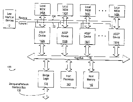
Referring now to Figure 1B, a network interface card CIVIC) 130 of a gateway
104 is illustrated. The NIC 130 includes one or more application-specific
signal
processors (ASSPs) 150A-150N. The number of ASSPs within a gateway is
expandable to handle additional channels. Line interface devices 131 of NIC
130
provide interfaces to various devices connected to the gateway, including the
network
101. In interfacing to the network 101, the line interface devices packetize
data for
transmission out on the network 101 and depacketize data which is to be
received by
the ASSP devices. Line interface devices 131 process information received by
the
gateway on the receive bus 134 and provides it to the ASSP devices.
Information from
the ASSP devices 150 is communicated on the transmit bus 132 for transmission
out of
the gateway. A traditional line interface device is a mufti-channel serial
interface or a
UTOPIA device. The NIC 130 couples to a gateway backplane/network interface
bus
I36 within the gateway 104. Bridge logic 138 transceiver information between
bus 136
11
CA 02422203 2003-03-06
WO 02/21855 PCT/USO1/27489
and NIC 130. Bridge logic 138 transceives signals between the NIC 130 and the
backplane/network interface bus 136 onto the host bus 139 for communication to
either
one or more of the ASSP devices 150A-150N, a host processor 140, or a host
memory
142. Optionally coupled to each of the one or more ASSP devices 150A through
150N
(generally referred to as ASSP 150) are optional local memory 145A through
145N
(generally referred to as optional local memory 145), respectively. Digital
data on the
receive bus 134 and transmit bus 132 is preferably communicated in bit wide
fashion.
While internal memory within each ASSP may be sufficiently large to be used as
a
scratchpad memory, optional local memory 145 may be used by each of the ASSPs
150
Z O if additional memory space is necessary.
Each of the ASSPs 150 provide signal processing capability for the gateway.
The type of signal processing provided is flexible because each ASSP may
execute
differing signal processing programs. Typical signal processing and related
voice
packetization functions for an ASSP include (a) echo cancellation; (b) video,
audio, and
voice/speech compression/decompression (voice/speech coding and decoding); (c)
delay handling (packets, frames); (d) loss handling; (e) connectivity (LAN and
WAN);
(fj security (encryption/decryption); (g) telephone connectivity; (h) protocol
processing
(reservation and transport protocols, RSVP, TCP/IP, RTP, UDP for IP, and AAL2,
AAL1, AALS for ATM); (i) filtering; (j) Silence suppression; (k) length
handling
(frames, packets); and other digital signal processing functions associated
with the
communication of voice and data over a communication system. Each ASSP 150 can
perform other functions in order to transmit voice and data to the various
endpoints of
the system 100 within a packet data stream over a packetized network.
Referring now to Figure 2, a block diagram of the ASSP 150 is illustrated. At
the heart of the ASSP 150 are four core processors 200A-200D. Each of the core
processors 200A-200D is respectively coupled to a data memory 202A-202D and a
program memory 204A-204D. Each of the core processors 200A-200D communicates
with outside channels through the mufti-channel serial interface 206, the
mufti-channel
memory movement engine 208, buffer memory 210, and data memory 202A-202D.
The ASSP 150 further includes an external memory interface 212 to couple to
the
external optional local memory 145. The ASSP 150 includes an external host
interface
214 for interfacing to the external host processor 140 of Figure 1B. - Further
included
within the ASSP 150 are timers 216, clock generators and a phase-lock loop
218,
12
CA 02422203 2003-03-06
WO 02/21855 PCT/USO1/27489
miscellaneous control logic 220, and a Joint Test Action Group (JTAG) test
access port
222 for boundary scan testing. The mufti-channel serial interface 206 may be
replaced
with a UTOPIA parallel interface for some applications such as ATM. The ASSP
150
further includes a microcontroller 223 to perform process scheduling for the
core
processors 200A-200D and the coordination of the data movement within the ASSP
as
well as an interrupt controller 224 to assist in interrupt handling and the
control of the
ASSP 150.
Referring now to Figure 3, a block diagram of the core processor 200 is
illustrated coupled to its respective data memory 202 and program memory 204.
Core
processor 200 is the block diagram for each of the core processors 200A-200D.
Data
memory 202 and program memory 204 refers to a respective instance of data
memory
202A-202D and program memory 204A-204D, respectively. The core processor 200
includes four signal processing units SPO 300A, SP1 300B, SP2 300C and SP3
300D.
The core processor 200 further includes a reduced instruction set computer
(RISC)
control unit 302 and a pipeline control unit 304. The~signal processing units
300A-
300D perform the signal processing tasks on data while the RISC control unit
302 and
the pipeline control unit 304 perform control tasks related to the signal
processing
function performed by the SPs 300A-300D. The control provided by the RISC
control
unit 302 is coupled with the SPs 300A-300D at the pipeline level to yield a
tightly
integrated core processor 200 that keeps the utilization of the signal
processing units
300 at a very high level.
The signal processing tasks are performed on the datapaths within the signal
processing units 300A-300D. The nature of the DSP algorithms are such that
they are
inherently vector operations on streams of data, that have minimal temporal
locality
(data reuse). Hence, a data cache with demand paging is not used because it
would not
function well and would degrade operational performance. Therefore, the signal
processing units 300A-300D are allowed to access vector elements (the
operands)
directly from data memory 202 without the overhead of issuing a number of load
and
store instructions into memory resulting, in very efficient data processing.
Thus, the
instruction set architecture of the present invention having a 20 bit
instruction word
which can be expanded to a 40 bit instruction word, achieves better
efficiencies than
VLIW architectures using 256-bits or higher instruction widths by adapting the
ISA to
DSP algorithmic structures. The adapted ISA leads to very compact and low-
power
13
CA 02422203 2003-03-06
WO 02/21855 PCT/USO1/27489
hardware that can scale to higher computational requirements. The operands
that the
ASSP can accommodate are varied in data type and data size. The data type may
be
real or complex, an integer value or a fractional value, with vectors having
multiple
elements of different sizes. The data size in the preferred embodiment is 64
bits but
larger data sizes can be accommodated with proper instruction coding.
Referring now to Figure 4, a detailed block diagram of the RISC control unit
302 is illustrated. RISC control unit 302 includes a data aligner and
formatter 402, a
memory address generator 404, three adders 406A-406C, an arithmetic logic unit
(ALU) 408, a multiplier 410, a barrel shifter 412, and a register file 413.
The register
file 413 points to a starting memory location from which memory address
generator
404 can generate addresses into data memory 202. The RISC control unit 302 is
responsible for supplying addresses to data memory so that the proper data
stream is
fed to the signal processing units 300A-300D. The RISC control unit 302 is a
register
to register organization with load and store instructions to move data to and
from data
1 S memory 202. Data memory addressing is performed by RISC control unit using
a 32-
bit register as a pointer that specifies the address, post-modification
offset, and type and
permute fields. The type field allows a variety of natural DSP data to be
supported as a
"first class citizen" in the architecture. For instance, the complex type
allows direct
operations on complex data stored in memory removing a number of bookkeeping
instructions. This is useful in supporting QAM demodulators in data modems
very
efficiently.
Refernng now to Figure SA, a block diagram of a signal processing unit 300 is
illustrated which represents an instance of the SPs 300A-300D. Each of the
signal
processing units 300 includes a data types and aligner 502, a first multiplier
M1 504A,
a compressor 506, a first adder A1 S l 0A, a second adder A2 S l OB, an
accumulator
register 512, a third adder A3 S l OC, and a second multiplier M2 504B. Adders
5 l0A-
5 l OC are similar in structure and are generally referred to as adder 510.
Multipliers
504A and 504B are similar in structure and generally referred to as multiplier
504.
Each of the multipliers 504A and 504B have a multiplexes 514A and 514B
respectively
at its input stage to multiplex different inputs from different busses into
the multipliers.
Each of the adders S 10A, S l OB, S l OC also have a multiplexes 520A, 520B,
and 520C
respectively at its input stage to multiplex different inputs from different
busses into the
adders. These multiplexers and other control logic allow the adders,
multipliers and
14
CA 02422203 2003-03-06
WO 02/21855 PCT/USO1/27489
other components within the signal processing units 300A-300C to be flexibly
interconnected by proper selection of multiplexers. In the preferred
embodiment,
multiplier Ml 504A, compressor 506, adder Al 510A, adder A2 S10B and
accumulator
512 can receive inputs directly from external data buses through the data
typer and
aligner 502. In the preferred embodiment, adder S l OC and multiplier M2 504B
receive
inputs from the accumulator 512 or the outputs from the execution units
multiplier Ml
504A, compressor 506, adder A1 510A, and adder A2 510B.
Program memory 204 couples to the pipe control 304 which includes an
instruction buffer that acts as a local loop cache. The instruction buffer in
the preferred
embodiment has the capability of holding four instructions. The instruction
buffer of
the pipe control 304 reduces the power consumed in accessing the main memories
to
fetch instructions during the execution of program loops.
Referring now to Figure 5B, a more detailed block diagram of the functional
blocks and the bus structure of the signal processing unit is illustrated.
Dyadic DSP ,
instructions are possible because of the structure and functionality provided
in each
signal processing unit. Output signals are coupled out of the signal processor
300 on
the Z output bus 532 through the data typer and aligner 502. Input signals are
coupled
into the signal processor 300 on the X input bus S31 and Y input bus 533
through the
data typer and aligner 502. Internally, the data typer and aligner 502 has a
different
data bus to couple to each of multiplier M1 504A, compressor 506, adder A1 S
10A,
adder A2 5 l OB, and accumulator register AR 512. While the data typer and
aligner
502 could have data busses coupling to the adder A3 S l OC and the multiplier
M2 504B,
in the preferred embodiment it does not in order to avoid extra data lines and
conserve
area usage of an integrated circuit. Output data is coupled from the
accumulator
register AR 512 into the data typer and aligner 502. Multiplier M1 504A has
buses to
couple its output into the inputs of the compressor 506, adder Al S 10A, adder
A2
510B, and the accumulator registers AR 512. Compressor 506 has buses to couple
its
output into the inputs of adder A1 S l OA and adder A2 S l OB. Adder A1 S l0A
has a bus
to couple its output into the accumulator registers 512. Adder A2 510B has
buses to
couple its output into the accumulator registers 512. Accumulator registers
512 has
buses to couple its output into multiplier M2 504B, adder A3 S l OC, and data
typer and
aligner 502. Adder A3 510C has buses to couple its output into the multiplier
M2 504B
and the accumulator registers 512. Multiplier M2 S04B has buses to couple its
output
CA 02422203 2003-03-06
WO 02/21855 PCT/USO1/27489
into the inputs of the adder A3 S l OC and the accumulator registers AR 512.
INSTRUCTION SET ARCHITECTURE
The instruction set architecture of the ASSP 150 is tailored to digital signal
processing applications including audio and speech processing such as
compression/decompression and echo cancellation. In essence, the instruction
set
architecture implemented with the ASSP 150, is adapted to DSP algorithmic
structures.
The adaptation of the ISA of the present invention to DSP algorithmic
structures is a
balance between ease of implementation, processing efficiency, and
programmability
of DSP algorithms. The ISA of the present invention provides for data movement
operations, DSP/arithmetic/logical operations, program control operations
(such as
function calls/returns, unconditional/conditional jumps and branches), and
system
operations (such as privilege, interrupt/trap/hazard handling and memory
management
control).
1 S Refernng now to Figure 6A, an exemplary instruction sequence 600 is
illustrated for a DSP algorithm program model employing the instruction set
architecture of the present invention. The instruction sequence 600 has an
outer loop
601 and an inner loop 602. Because DSP algorithms tend to perform repetitive
computations, instructions 605 within the inner loop 602 are executed more
often than
others. Instructions 603 are typically parameter setup code to set the memory
pointers,
provide for the setup of the outer loop 601, and other 2X20 control
instructions.
Instructions 607 are typically context save and function return instructions
or other
2X20 control instructions. Instructions 603 and 607 are often considered
overhead
instructions which are typically infrequently executed. Instructions 604 are
typically to
provide the setup for the inner loop 602, other control through 2x20 control
instructions, or offset extensions for pointer backup. Instructions 606
typically provide
tear down of the inner loop 602, other control through 2x20 control
instructions, and
combining of datapath results within the signal processing units. Instructions
605
within the inner loop 602 typically provide inner loop execution of DSP
operations,
control of the four signal processing units 300 in a single instruction
multiple data
execution mode, memory access for operands, dyadic DSP operations, and other
DSP
functionality through the 20/40 bit DSP instructions of the ISA of the present
invention.
Because instructions 605 are so often repeated, significant improvement in
operational
16
CA 02422203 2003-03-06
WO 02/21855 PCT/USO1/27489
efficiency may be had by providing the DSP instructions, including general
dyadic
instructions and dyadic DSP instructions, within the ISA of the present
invention.
The instruction set architecture of the ASSP 150 can be viewed as being two
component parts, one (RISC ISA) corresponding to the RISC control unit and
another
(DSP ISA) to the DSP datapaths of the signal processing units 300. The RISC
ISA is a
register based architecture including sixteen registers wi..;in the register
file 413, while
the DSP ISA is a memory based architecture with efficient digital signal
processing
instructions. The instruction word for the ASSP is typically 20 bits but can
be
expanded to 40-bits to control two RISC or DSP instructions to be executed in
series or
IO parallel, such as a RISC control instruction executed in parallel with a
DSP instruction,
or a 40 bit extended RISC or DSP instruction.
The instruction set architecture of the ASSP 150 has 4 distinct types of
instructions to optimize the DSP operational mix. These are (1) a 20-bit DSP
instruction that uses mode bits in control registers (i.e. mode registers),
(2) a 40-bit
15 DSP instruction having control extensions that can override mode registers,
(3) a 20-bit
dyadic DSP instruction, and (4) a 40 bit dyadic DSP instruction. These
instructions are
for accelerating calculations within the core processor 200 of the type where
D = [ (A
op 1 B) opt C ] and each of "op 1" and "opt" can be a multiply, add or
extremum
(minlmax) class of operation on the three operands A, B, and C. The ISA of the
ASSP
20 150 which accelerates these calculations allows efficient chaining of
different
combinations of operations. Because these type of operations require three
operands,
they must be available to the processor. However, because the device size
places limits
on the bus structure, bandwidth is limited to two vector reads and one vector
write each
cycle into and out of data memory 202. Thus one of the operands, such as B or
C,
25 needs to come from another source within the core processor 200. The third
operand
can be placed into one of the registers of the accumulator 512 or the RIS.C
register file
413. In order to accomplish this within the core processor 200 there are two
subclasses
of the 20-bit DSP instructions which are (1) A and B specified by a 4-bit
specifier, and
C and D by a 1-bit specifier and (2) A and C specified by a 4-bit specifier,
and B and D
30 by a 1 bit specifier.
Instructions for the ASSP are always fetched 40-bits at a time from program
memory with bit 39 and 19 indicating the type of instruction. After fetching,
the
instruction is grouped into two sections of 20 bits each for execution of
operations. In
17
CA 02422203 2003-03-06
WO 02/21855 PCT/USO1/27489
the case of 20-bit control instructions with parallel execution {bit 39=0, bit
19=0), the
two 20-bit sections are control instructions that are executed simultaneously.
In the
case of 20-bit control instructions for serial execution (bit 39=0, bit 19=1),
the two 20-
bit sections are control instructions that are executed serially. In the case
of 20-bit DSP
instructions for serial execution (bit 39=1, bit 19=1), the two 20-bit
sections are DSP
instructions that are executed serially. In the case of 40-bit DSP
instructions (bit 39=1,
bit 19=0), the two 20 bit sections form one extended DSP instruction which are
executed simultaneously.
The ISA of the ASSP 150 is fully predicated providing for execution
prediction.
Within the 20-bit RISC control instruction word and the 40-bit extended DSP
instruction word there are 2 bits of each instruction specifying one of four
predicate
registers within the RISC control unit 302. Depending upon the condition of
the
predicate register, instruction execution can conditionally change base on its
contents.
In order to access operands within the data memory 202 or registers within the
accumulator 512 or register file 413, a 6-bit specifies is used in the DSP
extended
instructions to access operands in memory and registers. Of the six bit
specifies used in
the extended DSP instructions, the MSB (Bit 5) indicates whether the access is
a
memory access or register access. In the preferred embodiment, if Bit 5 is set
to logical
one, it denotes a memory access for an operand. If Bit 5 is set to a logical
zero, it
denotes a register access for an operand. If Bit 5 is set to 1, the contents
of a specified
register (rX where X: 0-7) are used to obtain the effective memory address and
post-
modify the pointer field by one of two possible offsets specified in one of
the specified
rX registers. If Bit S is set to 0, Bit 4 determines what register set has the
contents of
the desired operand. If Bit-4 is set to 0, then the remaining specified bits
3:0 control
access to the registers within the register file 413 or to registers within
the signal
processing units 300.
DSP INSTRUCTIONS
There are four major classes of DSP instructions for the ASSP 150 these are
1) Multiply (MULT): Controls the execution of the main multiplier connected to
data
buses from memory.
Controls: Rounding, sign of multiply
18
CA 02422203 2003-03-06
WO 02/21855 PCT/USO1/27489
Operates on vector data specified through type field in address register
Second operation: Add, Sub, Min, Max in vector or scalar mode
2) Add (ADD): Controls the execution of the main-adder
Controls: absolute value control of the inputs, limiting the result
Second operation: Add, add-sub, mutt, mac, min, max
3) Extremum (MIN/MAX): Controls the execution of the main-adder
Controls: absolute value control of the inputs, Global or running maxlmin with
T
register, TR register recording control
Second operation: add, sub, mutt, mac, min, max
4) Misc: type-match and permute operations.
1.5 The ASSP 150 can execute these DSP arithmetic operations in vector or
scalar
fashion. In scalar execution, a reduction or combining operation is performed
on the
vector results to yield a scalar result. It is common in DSP applications to
perform
scalar operations, which are efficiently performed by the ASSP 150.
The 20-bit DSP instruction words have 4-bit operand specifiers that can
directly
access data memory using 8 address registers (r0-r7) within the register file
413 of the
RISC control unit 302. The method of addressing by the 20 bit DSP instruction
word is
regular indirect with the address register specifying the pointer into memory,
post-
modification value, type of data accessed and permutation of the data needed
to execute
the algorithm efficiently. All of the DSP instructions control the multipliers
504A-
504B, adders S l0A-S l OG, compressor 506 and the accumulator 512, the
functional
units of each signal processing unit 300A-300D.
In the 40 bit instruction word, the type of extension from the 20 bit
instruction
word falls into five categories:
1) Control and Specifier extensions that override the control bits in mode
registers
2) Type extensions that override the type specifier in address registers
3) Permute extensions that override the permute specifier for vector data in
address
registers
4) Offset extensions that can replace or extend the offsets specified in the
address
19
CA 02422203 2003-03-06
WO 02/21855 PCT/USO1/27489
registers
5) DSP extensions that control the lower rows of functional units within a
signal
processing unit 300 to accelerate block processing.
The 40-bit control instructions with the 20 bit extensions further allow a
large
immediate value (16 to 20 bits) to be specified in the instruction and
powerful bit
manipulation instructions.
Efficient DSP execution is provided with 2x20-bit DSP instructions with the
first 20-bits controlling the top functional units (adders 501A and 510B,
multiplier
504A, compressor 506) that interface to data buses from memory and the second
20
bits controlling the bottom functional units (adder 510C and multiplier 504B)
that use
internal or local data as operands. The top functional units, also referred to
as main
units, reduce the inner loop cycles in the inner loop 602 by parallelizing
across .
consecutive taps or sections. The bottom functional units cut the outer loop
cycles in
the outer Ioop 601 in half by parallelizing block DSP algorithms across
consecutive
samples.
Efficient DSP execution is also improved by the hardware architecture of the
present invention. In this case, efficiency is improved in the manner that
data is
supplied to and from data memory 202 to feed the four signal processing units
300 and
the DSP functional units therein. The data highway is comprised of two buses,
X bus
531 and Y bus 533, for X and Y source operands, and one Z bus 532 for a result
write.
All buses, including X bus 531, Y bus 533, and Z bus 532, are preferably 64
bits wide.
The buses are uni-directional to simplify the physical design and reduce
transit times of
data. In the preferred embodiment when in a 20 bit DSP mode, if the X and Y
buses are
both carrying operands read from memory for parallel execution in a signal
processing
unit 300, the parallel load field can only access registers within the
register file 413 of
the RISC control unit 302. Additionally, the four signal processing units 300A-
300D in
parallel provide four parallel MAC units (multiplier 504A, adder 510A, and
accumulator 512) that can make simultaneous computations. This reduces the
cycle
count from 4 cycles ordinarily required to perform four MACS to only one
cycle.
DYADIC DSP INSTRUCTIONS
All DSP instructions of the instruction set architecture of the ASSP 150 are
CA 02422203 2003-03-06
WO 02/21855 PCT/USO1/27489
dyadic DSP instructions within the 20 bit or 40 bit instruction word. A dyadic
DSP
instruction informs the ASSP in one instruction and one cycle to perform two
operations. Referring now to Figure 6B is a chart illustrating the
permutations of the
dyadic DSP instructions. The dyadic DSP instruction 610 includes a main DSP
operation 611 (MAIN OP) and a sub DSP operation 612 (SUB OP), a combination of
two DSP instructions or operations in one dyadic instruction. Generally, the
instruction
set architecture of the present invention can be generalized to combining any
pair of
basic DSP operations to provide very powerful dyadic instruction combinations.
Compound DSP operational instructions can provide uniform acceleration for a
wide
variety of DSP algorithms not just multiply-accumulate intensive filters. The
DSP
instructions or operations in the preferred embodiment include a multiply
instruction
(MULT), an addition instruction (ADD), a minimizelmaxirnize instruction
(MIN/MAX) also referred to as an extrema instruction, and a no operation
instruction
(NOP) each having an associated operation code ("opcode"). Any two DSP
instructions can be combined together to form a dyadic DSP instruction. The
NOP
instruction is used for the MAIN OP or SUB OP when a single DSP operation is
desired to be executed by the dyadic DSP instruction. There are variations of
the
general DSP instructions such as vector and scalar operations of
multiplication or
addition, positive or negative multiplication, and positive or negative
addition (i.e.
subtraction).
Referring now to Figure 6C and Figure 6D, bitmap syntax for an exemplary
dyadic DSP instruction is illustrated. Figure 6C illustrates bitmap syntax for
a control
extended dyadic DSP instruction while Figure 6D illustrates bitmap syntax for
a non-
extended dyadic DSP instruction. In the non-extended bitmap syntax the
instruction
word is the twenty most significant bits of a forty bit word while the
extended bitmap
syntax has an instruction word of forty bits. The three most significant bits
(MSBs),
bits numbered 37 through 39, in each indicate the MAIN OP instruction type
while the
SUB OP is located near the middle or end of the instruction bits at bits
numbered 20
through 22. In the preferred embodiment, the MAIN OP instruction codes are 000
for
NOP, 101 for ADD, 110 for MIN/MAX, and 100 for MULT. The SUB OP code for
the given DSP instruction varies according to what MAIN OP code is selected.
In the
case of MULT as the MAIN OP, the SUB OPs are 000 for NOP, 001 or 010 for ADD,
100 or 011 for a negative ADD or subtraction, 101 or 110 for MIN, and 111 for
MAX.
21
CA 02422203 2003-03-06
WO 02/21855 PCT/USO1/27489
In the preferred embodiment, the MAIN OP and the SUB OP are not the same DSP
instruction although alterations to the hardware functional blocks could
accommodate
it. The lower twenty bits of the control extended dyadic DSP instruction, the
extended
bits, control the signal processing unit to perform rounding, limiting,
absolute value of
inputs for SUB OP, or a global MIN/MAX operation with a register value.
The bitmap syntax of the dyadic DSP instruction can be converted into text
syntax for program coding. Using the multiplication or MULT non-extended
instruction as an example, its text syntax for multiplication or MULT is
(vmulwmuln).(vaddwsubwmax~sadd~ssub~smax) da, sx, sa, sy [,(ps0)Ipsl)]
The "vmulwmuln" field refers to either positive vector multiplication or
negative vector
multiplication being selected as the MAIN OP. The next field,
"vaddwsubwmax~sadd~ssub~smax", refers to either vector add, vector subtract,
vector
maximum, scalar add, scalar subtraction, or scalar maximum being selected as
the SUB
OP. The next field, "da", refers to selecting one of the registers within the
accumulator
for storage of results. The field "sx" refers to selecting a register within
the RISC
register file 413 which points to a memory location in memory as one of the
sources of
operands. The field "sa" refers to selecting the contents of a register within
the
accumulator as one of the sources of operands. The field "sy" refers to
selecting a
register within the RISC register file 413 which points to a memory location
in memory
as another one of the sources of operands. The field of "[,(ps0)~psl)]" refers
to pair
selection of keyword PSO or PS1 specifying which are the source-destination
pairs of a
parallel-store control register. Referring now to Figure 6E and 6F, lists of
the set of 20-
bit DSP and control instructions for the ISA of the present invention is
illustrated.
Figure 6G lists the set of extended control instructions for the ISA of the
present
invention. Figure 6H lists the set of 40-bit DSP instructions for the ISA of
the present
invention. Figure 6I lists the set of addressing instructions for the ISA of
the present
invention.
Refernng now to Figure 7, a block diagram illustrates the instruction decoding
for configuring the blocks of the signal processing unit 300. The signal
processor 300
includes the final decoders 704A through 704N, and multiplexers 720A through
720N.
The multiplexers 720A through 720N are representative of the multiplexers 514,
516,
520, and 522 in Figure SB. The predecoding 702 is provided by the RISC control
unit
302 and the pipe control 304. An instruction is provided to the predecoding
702 such
22
CA 02422203 2003-03-06
WO 02/21855 PCT/USO1/27489
as a dyadic DSP instruction 600. The predecoding 702 provides preliminary
signals to
the appropriate final decoders 704A through 704N on how the multiplexers 720A
through 720N are to be selected for the given instruction. Referring back to
Figure 5 B,
in a dyadic DSP instruction the MAIN OP generally, if not a NOP, is performed
by the
blocks of the multiplier M1 504A, compressor 506, adder Al S 10A, and adder A2
S l OB. The result is stored in one of the registers within the accumulator
register AR
S 12. In the dyadic DSP instruction the SUB OP generally, if not a NOP, is
performed
by the blocks of the adder A3 SIOC and the multiplier M2 504B. For example, if
the
dyadic DSP instruction is to perform is an ADD and MULT, then the ADD
operation of
the MAIN OP is performed by the adder Al S l0A and the SUB OP is performed by
the
multiplier M1 504A. The predecoding 720 and the final decoders 704A through
704N
appropriately select the respective multiplexers 720A through 720B to select
the MAIN
OP to be performed by the adder A1 S l0A and the SUB OP to be performed by the
multiplier M2 504B. In the exemplary case, multiplexes 520A selects inputs
from the
data types and aligner 502 in order for adder A1 S l0A to perform the ADD
operation,
multiplexes 522 selects the output from adder S l0A for accumulation in the
accumulator 512, and multiplexes 514B selects outputs from the accumulator 512
as its
inputs to perform the MULT SUB OP. The MAIN OP and SUB OP can be either
executed sequentially (i.e. serial execution on parallel words) or in parallel
(i.e. parallel
execution on parallel words). If implemented sequentially, the result of the
MAIN OP
may be an operand of the SUB OP. The final decoders 704A through 704N have
their
own control logic to properly time the sequence of multiplexes selection for
each
element of the signal processor 300 to match the pipeline execution of how the
MAIN
OP and SUB OP are executed, including sequential or parallel execution. The
RISC
control unit 302 and the pipe control 304 in conjunction with the final
decoders 704A
through 704N pipelines instruction execution by pipelining the instruction
itself and by
providing pipelined control signals. This allows for the data path to be
reconfigured by
the software instructions each cycle.
TELECOMMUNICATIONS PROCESSING
Referring now to Figure 10, a detailed system block diagram of the packetized
telecommunication communication network 100' is illustrated. In the packetized
23
CA 02422203 2003-03-06
WO 02/21855 PCT/USO1/27489
telecommunications network 100' an end system 108A is at a near end while an
end
system 108B is at a far end. The end systems 108A and/or 108B can be a
telephone, a
fax machine, a modem, wireless pager, wireless cellular telephone or other
electronic
device that operates over a telephone communication system. The end system
108A
couples to switch 106A which couples into gateway 104A. The end system 108B
couples to switch 106B which couples into gateway 104B. Gateway 104A and
gateway
104B couple to the packet network 101 to communicate voice and other
telecommunication data between each other using packets. Each of the gateways
104A
and 104B include network interface cards (NIC) 130A-130N, a system controller
board
1010, a framer card 1012, and an Ethernet interface card 1014. The network
interface
cards (NIC) 130A-130N in the gateways provide telecommunication processing for
multiple communication channels over the packet network 101. On one side, the
NICs
130 couple packet data into and out of the system controller board 1010. The
packet
data is packetized and depacketized by the system controller board 1010. The
system
controller board 1010 couples the packets of packet data into and out of the
Ethernet
interface card 1014. The Ethernet interface card 1014 of the gateways
transmits and
receives the packets of telecommunication data over the packet network 101. On
an
opposite side, the NICs 130 couple time division multiplexed (TDM) data into
and out
of the framer card 1012. The framer card 1012 frames the data from multiple
switches
106 as time division multiplexed data for coupling into the network interface
cards 130.
The framer card 1012 pulls data out of the framed TDM data from the network
interface cards I30 for coupling into the switches I06.
Each of the network interface cards 130 includes a micro controller (cPCI
controller) 140 and one or more of integrated telecommunications processors
150A-
150N. Each of the integrated telecommunications processors 150N includes one
or
more RISC/DSP core processor 200, one or more data memory (DRAM) 202, one or
more program memory (PRAM) 204, one or more serial TDM interface ports 206 to
support multiple TDM channels, a bus controller or memory movement engine 208,
a
global or buffer memory 210, a host or host bus interface 214, and a
microcontroller
(MIPS) 223. Firmware flexibly controls the functionality of the blocks in the
integrated
telecommunications processor 150 which can vary for each individual channel of
communication.
Referring now to Figure 1 lA, a block diagram of the firmware
24
CA 02422203 2003-03-06
WO 02/21855 PCT/USO1/27489
telecommunications processing modules of the application specific signal
processor
150, forming the "integrated telecommunications processor" 1 S0, for one of
multiple
full duplex channels is illustrated. One full duplex channel consists of two
time-
division multiplexed (TDM) time slots on the TDM or near side and two packet
data
channels on the packet network or far side, one for each direction of
communication.
The telecommunication processing provided by the firmware can provide
telephony
processing for each given channel including one or more of network echo
cancellation
1103, dial tone detection 1104, a fax processor 1119, voice activity detection
1105,
dual-tone mufti-frequency (DTMF) signal detection 1106; dual-tone mufti-
frequency
(DTMF) signal generation 1107; dial tone generation 1108; G.7xxx voice
encoding (i.e.
compression) 1109; G.7xxx voice decoding (i.e. decompression) 1110, and
comfort
noise generation (CNG) 1111. The firmware for each channel is flexible and can
also
provide GSM decoding/encoding, CDMA decoding/encoding, digital subscriber line
(DSL), modem services including modulation/demodulation, fax services
including
modulation/demodulation and/or other functions associated with
telecommunications
services for one or more communication channels. While -Law / A-Law decoding
1101 and -Law l A-Law encoding 1102 can be performed using firmware, in one
embodiment it is implemented in hardware circuitry in order to speed the
encoding and
decoding of multiple communication channels. The integrated telecommunications
processor 150 couples to the host processor 140 and a packet processor 1120.
The host
processor 140 loads the firmware into the integrated telecommunications
processor to
perform the processing in a voice over packet (VoP) network system or
packetized
network system.
The -Law l A-Law decoding 1101 decodes encoded speech into linear speech
data. The -Law / A-Law encoding 1102 encodes linear speech data into -Law / A-
Law encoded speech. The integrated telecommunications processor 150 includes
hardware 6.711 -Law / A-Law decoders and -Law / A-Law encoders. The
hardware conversion of A-law/ -law encoded signals into linear PCM samples and
vice versa is optional depending upon the type of signals received. Using
hardware for
this conversion is preferable in order to speed the conversion process and
handle
additional communication channels. The TDM signals at the near end are encoded
speech signals. The integrated telecommunications processor 150 receives TDM
signals from the near end and decodes them into pulse-code modulated (PCM)
linear
2s
CA 02422203 2003-03-06
WO 02/21855 PCT/USO1/27489
data samples 5;~. These PCM linear data samples S;" are coupled into the
network
echo-cancellation module 1103. The network echo-cancellation module 1103
removes
an echo estimated signal from the PCM linear data samples S;" to generate PCM
linear
data samples Souc. The PCM linear data samples So"c are provided to the DTMF
detection module 1106 and the voice-activity detection and comfort-noise
generator
module 1105. The output of the Network Echo Canceller (Sout) is coupled into
the
Tone Detection module 1104, the DTMF Detection module 1106, and the Voice
Activity Detection module 1105. Control signals from the Tone Detection module
1104 are coupled back into the Network Echo Cancellation module 1103. The
decoded
speech samples from the far end are PCM linear data samples Rin and are
coupled into
the network echo cancellation module 1103. The network echo cancellation
module
1103 copies R;~ for echo cancellation purposes and passes it out as PCM linear
data
samples R.o"c. The PCM linear data samples Ro"c are coupled into the mu-law
and A-
law encoding module 1102. The PCM linear data samples Ro"c are encoded into mu-
law and A-law encoded speech and interleaved into the TDM output signals of
the
TDM channel Output to the near end. The interleaving for framing of the data
is
performed after the linear to A-law/mu-law conversion by a Framer (not shown
in
Figure 11A) which puts the individual channel data into different time slots.
For
example, for Tl signaling there are 24 such time slots for each T1 frame.
The Network Echo Cancellation module 1103 has two inputs and two outputs
because it has full duplex interfaces with both the TDM channels and the
packet
network via the VX-Bus. The network echo cancellation module 1103 cancels
echoes
from linear as well as non-linear sources in the communication channel. The
network
echo cancellation module 1103 is specifically tailored to cancel non-linear
echoes
associated with the packet delays/latency generated in the packetized network.
The tone detection module 1104 receives both tone and voice signals from the
network cancellation module 1103. The tone detection module 1104 discriminates
the
tones from the voice signals in order to determine what the tones are
signaling. The
tone detection module determines whether or not the tones from the near end
are call
progress tones (dial tone, busy tone, fast busy tone, etc.) signaling on-hook,
ringing,
off hook or busy, or a fax/modem call. If a far end is dialing the near end,
the call
progress tones of on-hook, ringing, or off hook or busy signal is translated
into packet
signals by the tone detection module for transmission over the packet network
to the far
26
CA 02422203 2003-03-06
WO 02/21855 PCT/USO1/27489
end. If the tone detection module determines that fax/modem tones are present
indicating that the near end is initiating a faxlmodem call, further voice
processing is
bypassed and the echo cancellation by the network echo cancellation module
1103 is
disabled.
To detect tones, the tone detection module 1104 uses infinite impulse-response
(IIR) filters and accompanying logic. When a FAX or modem tone signaling tone
is
detected, the signaling tones help control the respective signaling event. The
tone
detection module 1104 detects the presence of several in-band tones at
specific
frequencies, checks their cadences, signals their presence to the echo
cancellation
module I 103, and prompts other modules to take appropriate actions. The tone
detection module 1104 and the DTMF detection module operate in parallel with
the
network echo canceller 1103.
The tone detection module can detect true tones with signal amplitude levels
from 0 dB to -40 dB in the presence of a reasonable amount of noise. The tone
detection module can detect tones within a reasonable neighborhood of center
frequency with detection delays within a prescribed limit. The tone detection
module
matches the tone cadences, as required by the tone-cadence rules defined by
the
ITU/TIA standards. To achieve the above properties, certain trade-offs are
necessary in
that the tone detection module must adjust several energy thresholds, the
filter roll-off
rate, and the filter stopband attenuation. Furthermore, the tone detection
module is
easily upgradeable to allow detection of additional tones simply by updating
the
firmware. The current telephony-related tones that the tone-detection module I
104 can
detect are listed in the following table:
27
CA 02422203 2003-03-06
WO 02/21855 PCT/USO1/27489
~ Tones the Tone-Detection Module Detects
one Name one Descri tion 'On' Time 'Off Time
FAX CED 2100 Hz 2.6 to 4 seconds
Echo 2100 Hz, with 2.6 to 4 seconds
phase
Cancellationreversal every
450 ms
Disable /
Modem Tones
FAX CNG 1100 Hz 0.5 seconds 3 seconds
FAX V.21 7E flags frequency-At least three
7E flags signal
the
shift keying at onset of a FAX
170-Hz signal being
sent.
Garner.
2400 Hz In-band signaling6.168 Test 8 describes
tones the
and continuity performance of
check echo cancellation
in
tones the presence of
these tones.
2600 Hz
When a 2100-Hz tone with phase reversal is detected indicating a V-series
modem
operation the echo canceller is shut off temporarily. When the tone detection
module
detects facsimile tones, the echo canceller is shut off temporarily. The tone
detection
module can also detect the presence of narrowband signals, which can be
control
signals to control the actions of the echo cancellation module 1103. The tone
detection
modules function both during call set up and while the call progress through
termination of the communication channel for the call. Any tone which is sent,
generated, or detected before the actual call or communication channel is
established, is
referred to as an out-of band tone. Tones which are detected during a call,
after the call
has been set-up, are referred to as in-band tones. The Tone Detector, in it's
most
general form, is capable of detecting many signaling tones. The tones that are
detected
include the call progress tones such as a Ringing Tone, a Busy Tone, a Fast
Busy Tone,
a Caller m Tone, a Dial Tone, and other signaling tones which vary from
country to
country. The, call progress tones control the handshaking required to set up a
call. Once
a call is established, all the tones which are generated and detected are
referred to as in-
band tones. The same Tone Detectors and Generators Blocks are used both for in-
band
and out-of band tone detection and generation.
Figure 11B illustrates a process 1121 for tone detection that can be
implemented
28
CA 02422203 2003-03-06
WO 02/21855 PCT/USO1/27489
by a tone detection processor/module according to one embodiment of the
invention.
As previously discussed, the tone detection module 1104 receives both tone and
voice
signals from the network cancellation module and discriminates the tones from
the
voice signals in order to determine what the tones are signaling. The tone
detection
module determines whether or not the tones are call progress tones (dial tone,
busy
tone, fast busy tone, etc.) signaling on-hook, ringing, off hook or busy, a
fax call signal,
or a modem call signal.
Upon start (block 1122), the process 1121 receives incoming tone and voice
data frames. A frame is composed of N samples of the incoming tone/voice
signal. In
one embodiment, a frame is composed of, for example, 120 samples. Frequency
resolution increases as the frame size increases. 120 samples was chosen to
optimize
both time and frequency resolution. The process 1121 operates on a frame by
frame
basis. The process 1121 first performs automatic gain control (AGC) (block
1124).
The principal of operation of the AGC is based on normalizing the power of the
incoming tone/voice signal to make sure that the gain is not so high that it
will overflow
the Goertzel filter. In doing so, the AGC computes the total energy (e.g.
Ex(n)~2).
Next, the process 1121 utilizes a Goertzel Filter process which implements a
plurality of Goertzel filters to determine the energy of the tone/voice signal
at specific
frequencies. The Goertzel filter is a type of discrete Fourier transform to
obtain a
power spectrum, as a function of frequency, for a given signal waveform. The
Goertzel
filter is a type of infinite impulse-response (IIR) filter and is well known
in the art.
These specific frequencies can be chosen by the user of the "integrated
telecommunications processor" 150. Figure 11C shows a table of common
frequencies
used in the telecommunications industry and associated exemplary coefficients
for the
Goertzel filter. Also, it should be appreciated that the user can define two
frequencies
to define dual-tone multi-frequency (DTMF) tones, as well as other
combinations of
frequencies, to define various tones.
In one embodiment, the Goertzel filter computes the energy levels of the
tone/voice signal at 16 specific frequencies. This takes advantage of the
architecture of
the integrated telecommunications processor 150. In one embodiment, the
integrated
telecommunications processor 150 includes a RISC/DSP core processor 200 that
includes four signal processors 300a-d that can operate in parallel to perform
four
Goertzel filters, simultaneously. Thus, in four cycles of the core processor
200, 16
29
CA 02422203 2003-03-06
WO 02/21855 PCT/USO1/27489
Goertzel filters can be computed to determine the energy levels of the
tone/voice signal
at the 16 specifc frequencies thereby achieving an efficiency of 4-1. However,
it
should be appreciated that the architecture of the integrated
telecommunications
processor 150 is scalable to include any number of core processors with each
core
processor having a greater number of signal processors that can be used
simultaneously
to perform mathematical computations such as the Goertzel filter.
Next, the process 1121 determines the state of the tone detection (block
1128).
The process 1121 includes three different states: TONE ON, TONE OFF, and TONE
ON/OFF. The state also includes a TONE ON counter that keeps track of the time
a
specific tone is recognized by the tone detection process 1121 and a TONE OFF
counter that that keeps track of the time after a tone has been recognized.
For ease of
illustration, the process 1 I21 will first be described assuming that a tone
has not yet
been recognized by the process 1121 and that the state is set to TONE OFF.
The process 1121 then finds the maximum energy level or levels of the
incoming tone/voice signal and their associated frequencies (block 1130).
Particularly,
the process 1121 determines the two maximum energy levels of the tone/voice
signal
and their associated frequencies from the Goertzel filter. In one embodiment,
the
process 1121 determines the two maximum energy levels of the tone/voice signal
and
their associated frequencies from the 16 specific frequencies (e.g. user
defined)
computed by the Goertzel filter.
In block 1132, the process 1121 based upon the calculation of the two
maximum energy levels discriminates whether the tone is a single tone, a dual
tone,
silence, or other (e.g. speech). In discriminating tones, the user can also
define specific
minimum energy levels at which to determine whether or not a tone exists (i.e.
tone
presence) for a given frequency. If a tone in block 1132 is not found, then
the process
1121 proceeds to the next frame (block 1140) and the process 1121 starts over
(block
1122). On the other hand, if a single or dual tone is detected, the process
1121 looks
for the detected single/dual tone in a user defined dictionary of the tones
(block 1134).
As previously discussed, a user can define a number of different frequencies
at
which to determine certain tones. In one embodiment, a user can define 16
frequencies
at which to determine whether certain tones are present. Figure 11D
illustrates a partial
dictionary of exemplary call progress tones. It should be appreciated that the
user
defined dictionary can also include many other sorts of tones such as the: FAX
CED,
CA 02422203 2003-03-06
WO 02/21855 PCT/USO1/27489
FAX CNG, and DTMF.
If the tone is found the dictionary (block 1134), the process 1121 updates the
state from TONE OFF to TONE ON (block 1138). The process 1121 then proceeds to
the next frame (block 1140) and the process 1121 starts over (block 1122) with
the state
set to TONE ON.
Upon start (block 1122) the process 1121 receives and processes the next
incoming tonelvoice data frames. The process 1121 then performs automatic gain
control (AGC) (block 1124), as previously described. Similarly, the process
1121
again utilizes a Goertzel filter to determine the energy of the next
tone/voice signal at
specific frequencies (block 1126), also as previously described. The process
1121 then
determines the state of the tone detection (block 1128). Continuing with the
current
example, at this point, the state is determined to be set to TONE ON and the
process
1121 proceeds to block 1142.
At block 1142, the process 1121 finds the maximum energy level or levels of
the next tone/voice signal and their associated frequencies in the same manner
as
previously described. Further, as previously described, the process 1121 based
upon
the calculation of the two maximum energy levels discriminates whether the
tone is a
single tone, a dual tone, silence, or other (e.g. speech) (block 1144). If no
tone is
detected then the process 1121 continues to block 1150. However, if a single
or dual
tone is detected, the process 1121 determines if it is the same tone as the
tone identified
in the dictionary (block 1146). If so, then state information is updated by
incrementing
the TONE ON counter (block 1148) and the process 1121 proceeds to the next
frame
(block 1140) and the process 1121 starts over (block 1122) with the state
still set to
TONE ON. On the other hand, if the same tone is not detected (block 1146) or
no tone
is detected (block 1144) then the process 1121 proceeds to block 1150.
At block 1150, the process 1121 determines whether an OFF cadence is defined
for the tone identified in the dictionary. An OFF cadence is a period of time,
set by a
user or defined by telecommunications standards, in which there should be
silence after
the end of the tone. An ON cadence is a period of time, set by a user or
defined by
telecommunications standards, during which the tone should be on. Although an
ON
cadence value is almost always defined for a tone, an OFF cadence value for a
tone
may or may not be defined. Returning again to block 1150, the process 1121
determines whether an OFF cadence is defined. If an OFF cadence is not
defined, then
31
CA 02422203 2003-03-06
WO 02/21855 PCT/USO1/27489
the process 1121 determines whether the tone identified in the dictionary was
on for the
period of time set by the ON cadence value (block 1152). If not, then the
process 1121
is reset (block 1154) and the process 1121 then proceeds to the next frame
(block 1140)
and the process 1121 starts over (block 1122). Reset generally involves the
initialization of the states and time counters. On the other hand, if the tone
identified in
the dictionary was on for the period of time set by the ON cadence value, then
a tone is
declared (block 1156). Next, the process 1121 is reset (block 1154) and the
process
1121 then proceeds to the next frame (block 1140) and the process 1121 starts
over
(block 1122).
Returning to block 1150, if an OFF cadence value is defined, then the state is
updated to TONE ON/OFF (block 1158). The process 1121 then proceeds to the
next
frame (block 1140) and the process 1121 starts over (block 1122) with the
state set to
TONE ON/OFF.
Upon start (block 1122) the process 1121 receives and processes the next
incoming tone/voice data frames. The process 1121 then performs automatic gain
control (AGC) (block 1124) and again utilizes a Goertzel filter to determine
the energy
of the next tone/voice signal at specific frequencies (block 1126), also as
previously
described. Next, the process 1121 determines the state of the tone detection
(block
1128). Continuing with the current example, at this point, the state is
determined to be
set to TONE ON/OFF and the process 1121 proceeds to block 1160. The process
1121
based upon the calculation of the two maximum energy levels discriminates
whether
the tone is a single tone, a dual tone, silence, or other (e.g. speech) (block
1160). If no
tone (i.e. silence) is detected then the process 1121 continues to block 1162.
At block
1162, the process 1121 updates the state information by incrementing the TONE
OFF
counter and the process 1121 proceeds to the next frame (block 1140) and the
process
1121 starts over (block 1122) with the state still set to TONE ON/OFF.
However, if a tone is detected, the process 1121 determines whether the tone
identified in the dictionary was on (as measured by the TONE ON counter) for
the
period of time defined by the ON cadence value (block 1152) and whether the
time
after the tone identified in the dictionary (as measured by the TONE OFF
counter)
satisfies the OFF cadence value. If not, then the process 1121 is reset (block
1154) and
the process 1121 then proceeds to the next frame (block 1140) and the process
1121
starts over (block 1122). On the other hand, if the tone identified in the
dictionary was
32
CA 02422203 2003-03-06
WO 02/21855 PCT/USO1/27489
on for the period of time set by the ON cadence value and was off for the
period of time
set by the OFF cadence value then a tone is declared (block 1168). Next, the
process
1121 is reset (block 1154) and the process 1121 then proceeds to the next
frame (block
1140) and the process 1121 starts over (block 1122).
The process 1121 that has been previously described takes advantage of the
architecture of the integrated telecommunications processor 150. In one
embodiment,
the integrated telecommunications processor 150 includes a RISC/DSP core
processor
200 that includes four signal processors 300a-d that can operate in parallel
to perform
four Goertzel filters, simultaneously. Thus, in four cycles of the core
processor 200, 16
Goertzel filters can be computed to determine the energy levels of the
tone/voice signal
at the 16 specific frequencies thereby achieving an efficiency of 4-1.
Figure 11E illustrates another process 1169 for tone detection that can be
implemented by a tone detection processor/module according to one embodiment
of the
invention. As previously discussed, the tone detection module 1104 receives
both tone
and voice signals from the network cancellation module and discriminates the
tones
from the voice signals in order to determine what the tones are signaling.
Also, the
tone detection module 1104 in implementing process 1169 operates in
conjunction with
the FAX processor 1119 (Figure 11A). The tone detection module determines
whether
or not the tones are call progress tones (dial tone, busy tone, fast busy
tone, ete.)
signaling on-hook, ringing, off hook or busy, a fax signal, or a modem signal.
Further,
the process 1169 particularly distinguishes FAX V.21 tones, modem tones, and
echo
cancellation (EC) disable tones. The process 1169 of Figure 11E can be used
alone
and/or in conjunction with the process 1121 of Figure 11B.
Additionally, when the process 1169 of Figure 11 E detects a modem tone
and/or EC disable tone, it automatically disables echo cancellation. Also,
when the
process 1169 detects a FAXCED tone (ANS), a FAXCNG tone, or a FAX V.21 it
disables voice processing and provides a data by-pass for FAX processing.
The process 1169 uses bandpass Infinite Impulse Response (IIR) filters to
detect
tones and voice signals. The bandpass IIR filter is used to filter an input
signal. The
process 1169 makes a decision as to whether a tone is present, and what the
tone is, or
whether a voice signal is present, based upon comparing the filtered energy to
the
energy of the input signal. The process 1169 is a sample based process so that
a
decision as to whether a tone is detected or not can potentially be made at
any sample.
33
CA 02422203 2003-03-06
WO 02/21855 PCT/USO1/27489
Because IIR filters need to maintain state variables that are calculated one
after the
other, a cycle optimized implementation for the recursive algorithm of the IIR
filter is
desirable. An advantage of the process 1169 according to one embodiment of the
present invention is that it allows for a cycle optimized implementation.
Particularly,
the architecture of the integrated telecommunications processor 150 includes a
core
RISC/DSP processor 200 having four signal processors 300a-d that can operate
in
parallel to perform four I1R filters, simultaneously. This allows the IIR
filters to be
calculated very efficiently in a cycle optimized implementation.
Also, as will be discussed, almost all the tone detection procedures are
similar
in nature to that of the basic process 1169, however, the process 1169
particularly
distinguishes FAX V.21 tones and modem/echo cancellation disable tones. The
detection of the FAX V.21 tone is based on a demodulation technique. Also, in
order to
further detect modem tones and/or echo cancellation disable tones, phase-
reversals are
uniquely tested for to more accurately detect these types of tones.
Referring again to Figure 11E, the input signal x(n) first undergoes automatic
gain control (AGC) at block 1170 in the process 1169. The principal operation
of the
AGC 1170 is based on normalizing the power of the incoming tone/voice signal
to
make sure that the gain is not so high that it will overflow the IIR filters.
Further, the
AGC normalizes the power of the signal within a frame of N samples. In doing
so, the
AGC computes the total energy (e.g. Ex(n)~2). This sort of scaling is
necessary to
accommodate the wide dynamic ranges of tones that need to be detected.
Continuing with reference to Figure 11E, the process 1169 at block 1172 next
performs filtering. In one embodiment, Elliptic BR filters are used to design
the
bandpass filters. In this embodiment, the order of the filter used is 4. For
implementing the elliptic IIR filters an efficient DFII structure is used as
shown in
Figure 11F. DFII generally stands for Direct Form II (2) implementation of the
IIR
filter. The following equations implement the biquad structure:
Y[n] = b10 * x[n] + dl l
dl l = bl l * x[n] - al 1 * y[n] + d12
d12 = b12 * x[n] - al2 * y[n]
34
CA 02422203 2003-03-06
WO 02/21855 PCT/USO1/27489
or in a more general form:
yo=xo
yi = bi0yi - t[n]+ Cli2[n -1]
Clit[n]=bityi-t[n~-aityi[n~+C~it[n-1~
di2[n]=bi2yi-1[n]-Cli2yi[n]
~lV +l~
i ~=1,2,..., 2
Y~n~ '- Y 'n 2 lJ [n]
C
where x[n], y[n] are the input sample and filter output sample at instant 'n'
respectively. The other parameters make up the filter coefficients and filter
delays (see
also Figure 11 F). The algorithm is essentially sample by sample rather than
frame by
frame. Thus, a sample by sample filtering is performed using the double biquad
structure. The input arguments to this filter would be the all the filter
coefficients and
the state variables as well as the input at present time. Elliptic IIR f lters
utilizing a
DFII structure are well known in the art.
Continuing with to reference to Figure 11E, the process 1169 next performs an
energy estimation of the filtered signal y(n) at block 1173 and an energy
estimation of
the input signal x(n) at block 1174. Thus, this stage gives an indication of
how much
energy is present in these signals. The energy estimation filters are
implemented as
' follows:
E[n] = aI x[n]I + (1- a)E[n -1] (Energy for input signal
x(n))
E[n] = aI y[n]I + (1- a)E[n -1] (Energy for y(n) filtered
signal)
The Energy equations for the input signal x(n) and output signal y(n) are made
into
1x16 matrices so that they can be combined with the energy computation stages
of all
CA 02422203 2003-03-06
WO 02/21855 PCT/USO1/27489
the other filters.
Next, as shown in Figure 11 E, a decision at decision block 1176 is made as to
whether or not a specific tone is present. The following are the conditions
that the
input signal x(n) and the filtered signal y(n) must satisfy, before a decision
can be made
as to whether or not a specific tone is present:
1 ) The input signal energy (Energy for x(n)) must be greater than a minimum
specified threshold, MINTHRESH;
2) The filtered signal energy (Energy for y(n)) multiplied by a threshold must
be
greater than the input signal energy; and
3) The input signal must maintain an energy level which is adaptively updated
by the process, otherwise, the tone will be declared as absent.
Assuming the above conditions are satisfied, a tone will be detected and
declared as present (block 1178). An advantage of the present invention is
that it
allows for a cycle optimized implementation. Particularly, the architecture of
the
1 S integrated telecommunications processor 150 includes a core RISC/DSP
processor 200
having four signal processors 300a-d that can operate in parallel to perform
four IIR
filters, simultaneously. This allows the 1IR filters to be calculated very
efficiently in a
cycle optimized implementation. .Also, it should be noted that when the
process 1169
detects a FAXCED tone (ANS) or a FAXCNG tone, it disables voice processing and
provides a data by-pass for FAX processing.
However, even though a tone is detected, there are two special cases where
extra detection needs to be performed to ensure that the particular tones are
actually
present. These tones are the modem/echo cancellation disable tones and the FAX
V.21
tones. The process 1169 particularly distinguishes the modem/echo cancellation
disable tones and the FAX V.21 tones.
Thus, assuming a signal that has the characteristics of a modem/echo
cancellation disable tone (e.g. operation at 2100 Hz) is present, the process
1169
proceeds to block 1179 for further modem signal processing. For example,
modem/echo cancellation disable tones operate at 2100 Hz but so do other
signals, such
as the FAX CED tone. Thus, presently, there is no way to truly distinguish the
modemlecho cancellation disable tones. However, the process 1169 according to
one
embodiment of the present invention includes a further modem processing block
1179
which includes a method for phase reversal detection to ensure that the signal
has all
36
CA 02422203 2003-03-06
WO 02/21855 PCT/USO1/27489
the characteristics of a modem/echo cancellation disable tone. Particularly,
modem/echo cancellation disable tones have a phase reversal every 450 ms and
the
process 1169 checks for these phase reversals.
The sub-process for phase reversal detection 1181, shown in Figure 11 G, is
implemented by the process 1169 as part of the further modem processing block
1179.
The sub-process for phase reversal detection 1181 basically looks for a
negative spike
that is immediately followed by a positive spike. Figure 11 G also shows the
energy of
the signal (Es), the energy of the filtered signal (Ef), and the difference
(diffJ function
of the filtered energy from the original energy (i.e. the IIR filter), to
further illustrate
the sub-process for phase reversal detection 1181. To detect the spikes, the
sub-process
1181 checks if the value of the diff function is less than a negative
threshold (block
1182), for example -0.15 (see 1183 on the graph of the difference function).
If not, the
sub-process 1181 ends. However, if so, then the sub-process 1181 checks for a
positive
spike by checking if the diff function has a value greater than a positive
threshold
(block 1184), for example 0.1 (see 1185 on the graph of the difference
function). If not,
the sub-process 1181 ends. On the other hand, if this kind of valid transition
from
negative to positive spike exists then we conclude that a phase reversal took
place
(block 1186). The threshold is made adaptive by using the fact that the diff
function is a
function of the filtered energy. An adaptive threshold enables the sub-process
1 I8I to
have a wide dynamic range for the tone to be detected.
Advantageously, the sub-process 1181 specifically distinguishes the
modem/echo cancellation disable tones from other tones such as the FAX CED
tone
which may have the same frequency (e.g. 2100 Hz) but that do not have the same
phase
reversal characteristics. The unique sub-process 1181 emphasizes finding blips
in the
difference function so that phase-reversal detection is robust. One technique
used to
accomplish this is basically to pass the energy of the filtered signal through
a high-pass
filter and as shown in the Figure 11 G the blips are really emphasized and are
easily
detectable. Additionally, when the process 1169 of Figure 11E detects a modem
tone
and/or EC disable tone, it automatically disables echo cancellation.
Referring again to Figure 11E, even though a tone is detected (e.g. a tone
operating at a frequency of 1750 Hz) and it is believed to be a FAX V.21 tone,
the
process 1169 performs further detection to ensure that it is indeed a FAX V.21
tone.
The FAX V.21 tone has the characteristics of including basically 7E
(hexadecimal)
37
CA 02422203 2003-03-06
WO 02/21855 PCT/USO1/27489
flags sent at 300 bps. The binary signal is Frequency Shift Key (FSK)
modulated
around a carrier frequency of 1750 Hz. The frequency shift is +100 Hz for a
binary
zero and -100Hz for a binary one. Thus, assuming a signal that has the
characteristics
of a V.21 FAX modem tone (e.g. operating at a frequency of 1750 Hz) is
present, the
process 1169 proceeds to block 1180 for further fax processing to ensure that
it is
indeed a V.21 FAX modem tone.
Furthermore, with the growth of the Internet and packet based telephony, there
exists a strong need for an efficient mechanism for FSK demodulation. More
specifically, the V.21 FAX standard requires specific modulated data and a
carrier
frequency in order to convey that a call contains FAX data rather than voice.
The
demodulator of this signal needs to be relatively insensitive to reasonable
amounts of
noise and frequency offsets, and must properly capture the output codewords.
Similarly, the device must recognize when the tone has terminated.
A sub-process for fax V.21 detection 1199 according to embodiment of the
invention, shown in Figure 11H, satisfies the above requirements and
demodulates the
signal in a minimal amount of time and further detects the 7E flags robustly
even with
noise and frequency offset. The sub-process for fax V.21 detection is
implemented by
the process 1169 as part of the further Fax processing block 1179 (Figure 1
lE). In one
embodiment, the fax processor 1119 in conjunction with tone detection module
1104
(Figure 11A) executes the sub-process for fax V.21 detection 1199.
As shown in Figure 11H, the digitized input (e.g. y(n)) is received by the
mixer
1189. As previously discussed the digitized input is modulated using FSK with
a
carrier frequency of 1750 Hz. The first stage in the sub-process for fax V.21
detection
1199 is to begin demodulation of the signal by removing the carrier. This is
accomplished with the mixer (block 1189). The mixer 1189 mixes the data with a
stored copy of the carrier frequency. One input is mixed to baseband in one
cycle.
More specifically, the four inputs are multiplied by four cosine samples and
stored to
memory in one cycle. This can be done twice a loop with two extra instructions
for
control code. Therefore, there are eight cosines multiplies in fours cycles.
The same is
then done with a sine wave of the same frequency. Thus eight samples are mixed
with
sine and cosine in eight cycles (two separate loops), or one output per cycle.
The
outputs of the mixer stage 1188 are known as the in-phase and quadrature
components
of the signal.
38
CA 02422203 2003-03-06
WO 02/21855 PCT/USO1/27489
The second stage in the sub-process for fax V.21 detection 1199, i.e. the
lowpass filter (block 1190), may be needed if the signal quality is poor. The
lowpass
filter (block 1190) removes most of the high frequency noise content. Both the
in-
phase and quadrature component can be passed through the lowpass filter to
remove
noise. One lowpass filter (LPF) output is completed in (N/8) + 2 cycles. Two
outputs
are simultaneously calculated by using the data from two previous
instructions. This
permits the architecture of the integrated telecommunications processor 150 to
operate
eight multipliers in one cycle, utilizing the four signal processors (300a-d),
simultaneously, for a highly efficient implementation of an FIR filter.
The third stage in the sub-process for fax V.21 detection 1199, i.e. the phase
detector (block 1191), is where the original modulated signal is actually
recovered. A
simple mathematical difference equation is used in order to find the phase
difference
between each two successive baseband samples. Some noise may be introduced in
the
process since the two signals are not guaranteed to be of the same magnitude,
and may
have some residual noise not removed by the first filter. This phase
difference contains
a version of the original modulated signal. Particularly, one phase bit is
detected in .5
cycles. The formula for detecting a specific phase bit is:
I(N)*Q(N+1) - I(N+1)*Q(N). The architecture of the integrated
telecommunications
processor 150, utilizing the four signal processors (300a-d), simultaneously,
allows for
the completion of this operation in two cycles for four simultaneous outputs,
since four
multipliers are active in a given cycle.
The fourth stage in the sub-process for fax V.21 detection 1199, i.e. the
lowpass
filter (LPF) to prevent aliasing (block 1192), is similar to the second stage
in some
respects. The LPF to prevent aliasing (block 1192) not only eliminates high
frequency
noise content, but also prevents distortion known as aliasing when the sample
rate is
reduced.
The fifth stage in the sub-process for fax V.21 detection 1199 includes
reducing
the sample rate (block 1193). The sample rate is reduced to one sample per
modulated
symbol by taking every Nth sample and discarding the rest.
Finally, in the sixth stage of the sub-process for fax V.21 detection 1199 the
codewords are counted (block 1195). Particularly, the sign of the outputs are
collected
and counted one after another. If the pattern '7E' in hexadecimal is seen
three
consecutive times, the V21 flag is set to true. Otherwise, the flag goes back
to reset
39
CA 02422203 2003-03-06
WO 02/21855 PCT/USO1/27489
state until the next three '7E' codewords occur. If the V21 flag is set to
true, then it is
determined that FAX V.21 is present (block 1196).
The sub-process for fax V.21 detection 1199 includes many advantages. For
example, the sub-process detects the 7E flag robustly even with noise and
frequency
offset. Further, full demodulation occurs in 12 cycles per output. Also, the
sub-process
for fax V.21 detection 1199 utilizing the architecture of the integrated
telecommunications processor 150 performs high density filtering, mixing, and
phase
detection. Additionally, the sub-process can be used to demodulate generic FSK
modulated signals with a large enough sample rate, such that the approximation
sin(phase) = phase can be made. Also, when the FAX V.21 tone is verifed, voice
processing is disabled and a data by-pass is provided for FAX processing.
Turning away from tone detection and back to voice processing issues, in most
conversations, speakers only voice speech about 35% of the time. During the .
remaining 65% of the time in most conversations, a speaker is relatively
silent due to
natural pauses for emphasis, clarity, breathing, thought processes, and so
forth. When
there are more than two speakers, as in conference calls, there is even more
periods of
silence. It is an inefficient use of a communication channel to transmit
silence from
one end to another. Thus, statistical multiplexing techniques are used to
allocate to
other calls this 65% of'quiet' time (also known as 'dead time' or 'silence').
Even
though quiet time is allocated to other calls, the channel quality during the
time that end
users use the communication channel is preserved. However, silence at one end,
which
is not transmitted to an opposite end, needs to be simulated and inserted into
the call at
the opposite end.
Sometimes when we speak over a telephone, we hear the echo of our own
speech, which we usually ignore. The important point is that we do hear the
echo.
However, many digital telephone connections are so noise-free there is no
background
noise or residual echo at all. As a result a far-end user, hearing absolute
silence, may
think the connection is broken and hang up.
Returning again to Figure 11 a, to convince users there is a connection, the
background or Comfort-Noise Generation (CNG) module 1105 simulates silence or
quite time at an end by adding background noise such as a comforting 'hiss'.
The CNG
module 1105 can simulate ambient background noise of varying levels. An echo-
cancellation setup message can be used to control the CNG module as an
external
CA 02422203 2003-03-06
WO 02/21855 PCT/USO1/27489
parameter. The comfort noise generation module alleviates the effects of
switching in
and out as heard by far-end talkers when they stop talking. The near-end noise
level is
used to determine an appropriate level of background noise to be simulated and
inserted
at the SOut (Send Out) Port. However before silence can be simulated by the
CNG
module 1105, it first must be detected.
The Voice-Activity Detection (VAD) module 1105 is used to detect the
presence or absence of silence in a speech segment. When the VAD module 1105
detects silence, background noise energy is estimated and an encoder therein
generates
a Silence-Insertion Description (SID) frame. The SID frame is transmitted to
an
opposite end to indicate that silence is to be simulated at the estimated
background
noise energy level. In response to receiving an SID frame at the opposite end
(i.e., the
Far End), the CNG module 1111 generates a corresponding comfort noise or
simulated
silence for a period of time. Using the received level of the ambient
background noise
from the SID frame, the CNG produces a level of comfort noise (also called
'white
noise' or 'pink noise' or simulated silence) that replaces the typical
background noises
that have been removed, thereby assuring the far-end person that the
connection has not
been broken. The VAD module 1105 determines when the comfort noise is to be
turned on (i.e. a quiet period is detected) and when comfort noise is to be
turned off
(i.e. the end user is talking again). The VAD 1105 (in the Send Path) and CNG
module
1 I 1 I (in the Receive Path) work effectively together at two different ends
so that
speech is not clipped during the quiet period and comfort noise is
appropriately
generated.
The VAD module 1105 includes an Adaptive Level Controller (ALC) that
ensures a constant output level for varying levels of near-end inputs. The
adaptive
level controller includes a variable gain amplifier to maintain the constant
output level.
The adaptive level controller includes a near-end energy detector to detect
noise in the
near-end signal. When the near end energy detector detects noise in the near-
end signal
the ALC is disabled so that undesirable noise is not amplified.
The DTMF detection module 1106 performs dual-tone multiple frequency
detection necessary to detect DTMF tones as telephone signals. The DTMF
detection
module receives signals on Sout from the echo cancellation module 1103. The
DTMF
detection module 1106 is always active, even during normal conversation in
case
DTMF signals are transmitted during a conversation. The DTMF detection module
41
CA 02422203 2003-03-06
WO 02/21855 PCT/USO1/27489
does not disable echo cancellation when DTMF tones are detected. The DTMF
detection module includes narrow-band filters to detect special tones and DTMF
dialing tones.. Furthermore because the G.7xxx speech encoding module 1109 and
decoding module 1110 are used to compress/decompress speech signals and are
not
used for control signaling or dialing tones, the DTMF detection module may be
used as
appropriate to control sequencing, loading, and the execution of CODEC
firmware.
The DTMF detection module 1106 detects the DTMF tones and includes a
decoder to decode the tones to determine which telephone keypad button was
pressed.
The DTMF detection module 1106 is based on a Goertzel algorithm and meets all
conditions of the Bellcore DTMF decoder tests as well as Mitel decoder tests.
The DTMF detection module 1106 indicates which dialpad key a sender has
pressed after processing a few frames of data. The DTMF detection module can
be
adapted to receive user-defined parameters. The user defined parameters can be
varied
to optimize the DTMF detector for specific receiving conditions such as the
thresholds
for both of the frequencies made up by the'rows' and'columns' of the DTMF
keypad,
thresholds for acceptable twist ratios (the ratio of powers between the higher
and lower
frequencies), silence level, signal-to-noise ratios, and harmonic ratios.
The DTMF generation module 1107 provides dual-tone multiple frequency (DTMF)
generation necessary to generate DTMF tones for telephone signals. The
encoding
process in the DTMF generation module I 107 generates one of the various pairs
of
DTMF tones. The DTMF generation module 1107 generates digitized dual-tone
multi-
frequency samples for a dialpad key depression at the far end. The DTMF
generation
module 1107 is also always active, even during normal conversation. The DTMF
generation module 1107 includes narrow-band alters to generate special tones
and
DTMF dialing tones. The DTMF generation module 1107 receives a DTMF packet
from the far end over the packet network. The DTMF generation module 1107
includes a DTMF decoder to decode the DTMF packet and properly generate tones.
The DTMF packet payload includes such information as the key or digit that was
pressed that is to be played (i.e. dialpad key coordinates), duration to be
played
(Number of successive 125 microsecond samples during which the tone is enabled
and
Number of successive 125 microsecond samples during which the tone is shut off
disabled), amplitude level (Lower-frequency amplitude level in dB and Upper
frequency amplitude level in dB) and other information. By specifying these
42
CA 02422203 2003-03-06
WO 02/21855 PCT/USO1/27489
parameters, the DTMF generation module 1107 can generate DTMF signaling tones
having the required signal amplitude levels and timing for the appropriate
digit/tone.
The DTMF tones generated by the DTMF generation module 1107 are coupled into
the
echo canceller on Rin.
The tone generation module 1108 operates similar to the DTMF generation
module 1107 but generates the specific tones that provide telephony signals.
The tones
generated by the tone generation module include tones to signal On-hook/off
hook,
Ringing, Busy, and special tones to signal FAX/modem calls. A tone packet is
received from the far end over the packet network and is decoded and the
parameters of
the tone are determined. The tone generation module 1108 generates tone
similar to the
DTMF generation module 1107 previously described using narrowband filters.
The G.7xx encoding module 1109 provides speech compression before being
packetized. The G.7xx encoding module 1109 receives speech in a linear 64-Kbps
pulse-code modulation (PCM) format from the network echo cancellation module
1103. The speech is compressed by the G.7xx encoding module 1109 using one of
the
compression standards specified for low bit-rate voice (LBRV) CODECs,
including the
ITU-T internationally standardized G.7xx series. Many speech CODECs can be
chosen.
However, the selected speech CODEC determines the block size of speech samples
and
the algorithmic delay. Of several industry-standard speech CODECs in use, each
implements a different combination of Coding rate, Frame length (the size of
the
speech sample block), and Algorithmic delay (or detection delay) caused by how
long it
takes all samples to be gathered for processing.
The G.7xx decoding module 1110 provides speech decompression of signals
received from the far end over the packet network. The decompressed speech is
coupled into the network echo cancellation module 1103. The decompression
algorithm of the G.7xx decoding module 1110 needs to match the compression
algorithm of the G.7xx encoding module 1109. The G.7xx decoding module 1110
and
the G.7xx encoding module 1109 are referred to as a CODEC (coder-decoder).
Currently, there are several industry-standard speech CODECs from which to
pick.
The parameters for selection of a CODEC are previously described. The ITU
CODECs
include 6.711, 6.722, 6.723.1, 6.726, 6.727, 6.728, 6.729, G.729A, and G.728E.
Each of these can easily be selected by choice of firmware.
Data enters and leaves the processor 150 through the TDM serial I/O ports and
a
43
CA 02422203 2003-03-06
WO 02/21855 PCT/USO1/27489
32-bit parallel VX-Bus 1112. Data processing in the processor 150 is performed
using
16-bits of precision. The companded 8-bit PCM data on the TDM channel input is
converted into 16-bit linear PCM for processing in the processor 150 and is re-
converted back into 8-bit PCM for outputting on the TDM channel output.
Refernng now to Figure 12, a flow chart diagram of the telephony processing of
linear data (S;~) from a near end to packet data on the network side at a far
end is
illustrated. Near in data S;~ is provided to the integrated telecommunications
processor
150. At step 1201, a determination is made whether the echo cancellation
module 1103
is enabled or not. If the echo cancellation module 1103 is not enabled, the
integrated
telecommunications processor 150 jumps to the tone detection module 1205 which
detects the presence or absence of in-band tones in the Sin signal. If the
echo
cancellation module 1103 is enabled at step 1201, the near in data S;" is
coupled into
the echo cancellation module 1003 at step 1203 and data from the far end
(Farm) is
utilized to cancel out echoes. After echo cancellation is performed at step
1203 and/or
if the echo cancellation module 1103 is enabled, the integrated
telecommunications
processor 150 jumps to the tone detection step 1205 where the data is coupled
into tone
detection module 1104. Methods for tone detection (including fax tone
detection) have
been discussed previously with reference to Figures 11A-H. The processor 150
goes to
step 1207.
At step 1207, a determination is made whether a fax tone is present. If the
fax
tone is present at step 1207, the integrated telecommunications processor 150
jumps to
step 1209 to provide fax processing. If no fax tone is present at step 1207,
further
interpretation of the result by the tone detection module occurs at step 1211.
At step 1211, a determination is made whether there is an echo cancellation
control tone to indicate the Enabling and Disabling of the Echo Canceller. If
an Echo
cancellation control tone is present, integrated telecommunications processor
jumps to
step 1215. If no echo cancellation control tone is detected at step 1211, the
incoming
data signal Sin may be a voice or speech signal and the integrated
telecommunications
processor jumps to the VAD module at step 1219.
At step 1215 the energy of the Tone is compared to a predetermined threshold.
A determination is made whether or not the energy level in the signal S;" is
less than a
threshold level. If the energy of the Tone on S;" is greater than or equal to
this
predetermined threshold, the processor jumps to step 1213. If the energy of
the Tone
44
CA 02422203 2003-03-06
WO 02/21855 PCT/USO1/27489
on S;" is less than the threshold level, the integrated telecommunications
processor 1 ~0
jumps to step 1217.
At step 1213, the echo cancellation disable tone has been detected and the
energy of the tone is greater than a given predetermined threshold which
causes the
echo cancellation module to be disabled to cancel newly arnving Sin signals.
After the
Echo Canceller Disable Tone has been detected, the Echo Canceller block is
given an
indication through a control signal to disable Echo Cancellation.
At step 1217, the echo cancellation disable tone was not detected and the
energy
of the tone is less than the given predetermined threshold. The echo
cancellation
module is enabled or remains enabled if already in such state. The Echo
Canceller
block is given an indication through a control signal to enable Echo
Cancellation. This
may indicate the end of Echo Canceller Disable Tone.
The predetermined threshold level is a cutoff level to determine whether or
not
an Echo Canceller Disable Flag should be turned OFF. If the Tone Energy drops
below
a predetermined threshold, the Echo Cancellation disable flag is turned OFF.
This flag
is coupled into the Echo Canceller module. The Echo Canceller module is
enabled or
disabled in response to the echo cancellation disable flag. If the Tone energy
is greater
than the pre-determined threshold, then the processor jumps to step 1213 as
described
above. In either case, whether or not the echo cancellation disable flag is
set true or
false or at steps 1213 or 1217, the next step in processing is the VAD module
at step
1219.
At step 1219, the data signal Sin is coupled into the voice activity detector
module 1105 which is used to detect periods of voice/DTMF/tone signals and
periods
of silence that may be present in the data signal Sin. The processor 150 jumps
to step
1221.
At step 1221, a determination is made whether silence had been detected. If
silence has been detected, the integrated telecommunications processor 150
jumps to
step 1223 where an SID packet is prepared for transmission out as a packet on
the
packet network at the far end. If no silence is detected at step 1221, the
processor
couples the signal Sin into the ambient level control (ALC) module (not shown
in FIG.
11). At step 1225, the ALC amplifies or de-amplifies the signal S;~ to a
constant level.
Integrated telecommunications processor 150 then jumps to step 1227 where
DTMF/Generalized Tone detection is performed by the DTMF/Generalized Tone
CA 02422203 2003-03-06
WO 02/21855 PCT/USO1/27489
detection module 1106. The processor goes to step 1229.
At step 1229 a determination is made whether DTMF or tone signals have been
detected. If DTMF or tone signals have been detected, integrated
telecommunications
processor 150 generates DTMF or tone packets at step 1231 for transmission out
the
packet network at the far end. If no DTMF or tone signals are detected at step
1229,
the signal N is a voice/speech signal and the G.7XX encoding module 1109
encodes the
speech into a speech packet at step 1233. A speech packet 1235 is then
transmitted out
the packet network side to the far end.
Refernng now to figure 13, a flow chart diagram of the telephony processing of
packet data from the network side at the far end by the integrated
telecommunications
processor 150 into Ro"t signals at the near end is illustrated. The integrated
telecommunications processor 150 receives packet data from the far end over
the
packet network 101. At step 1301, a determination is made as to what type of
packet
has been received. The integrated telecommunications processor 150 is
expecting one
of five types of packets. The five packet types that are expected are a fax
packet 1303,
a DTMF packet 1304, a Tone packet 1305, a speech or SID packet 1306.
If at step 1301 a determination has been made that a fax packet 1303 has been
received, data from the packet is coupled into a fax demodulation module by
the
integrated telecommunications processor at step 1308. At step 1308, the fax
demodulation module demodulates the data from the packet using fax
demodulation
into Rout signals at the near end. If at step 1301 a determination has been
made that a
DTMF packet 1304 has been received, the data from the packet is coupled into
the
DTMF generation module 1107 at step 1310. At step 1310, the DTMF generation
module 1107 generates DTMF tones from the data in the packet Rout signals at
the
near end. If at step 1301 the packet received is determined to be a tone
packet 1305,
the data from the packet is coupled into the tone generation module 1108 at
step 1312.
At step 13 I2, the tone generation module 1108 generates tones as Rout signals
at the
near end. If at step 1301 a determination has been made that speech or S)D
packets
1306 have been received, the data from the packet is coupled into the G.7xx
decoding
module 1110 at step 1314. At step 1314, the G.7xx decoding module 1110
decompresses the speech or SID data from the packet into Rout signals at the
near end.
If at step 1301 a determination has been made that the packet is either a DTMF
46
CA 02422203 2003-03-06
WO 02/21855 PCT/USO1/27489
packet 1304, a tone packet 1305, a speech packet or an SID packet 1306, the
integrated
telecommunications processor 150 jumps to step 13 t 8. If at step 1318, the
echo
canceller flag is enabled, the Ro"~ signals from the respective module is
coupled into the
echo cancellation module. These Root signals are the Far End Input to the Echo
Canceller whose echo, if not cancelled, rides on the Near End Signal when it
gets
transmitted to the other end. At step 1318, the respective Ro~~ signal from a
module in
conjunction with the S;" signal and the Echo Canceller Enable Flag from the
nearend is
used to perform echo canceling. The Echo Canceller Enable Flag is a binary
flag which
turns ON and OFF the Echo Canceling operation in step 1318. When this flag is
ON,
the NearEndIn signals are processed to cancel the potential echo of the
FarEnd. When
this flag is OFF, the NearEndIn signal by-passes the Echo Canceling as is.
Referring now to Figure 14, a block diagram of the data flows and interaction
between exemplary functional blocks of the integrated telecommunications
processor
1 SO for telephony processing is illustrated. There are two data flows in the
voice over
packet (VOP) system provided by the integrated telecommunications processor
150.
The two data flows are TDM-to-Packet and Packet-to-TDM which are both executed
in
tandem to form a full duplex system.
The functional blocks in the TDM-to-Packet data flow includes the Echo
Canceller 1403, the tone detector 1404, the voice activity detector (VAD)
1405, the
automatic level controller (ALC) 1401, DTMF detector 1405, and packetizer
1409.
The Echo Canceller 1403 substantially removes a potential echo signal from the
near
end of gateway. The Tone Detector 1404 controls the echo canceller and other
modules of the integrated telecommunications processor 150. The tone detector
is for
detecting the EC Disable Tone, the FAXCED tone, the FAXCNG tone and V21 '7E'
flags. The tone detector 1404 can also be programmed to detect a given number
of
signaling tones also. The VAD 1405 generates Silence Information Descriptor
(SID)
when speech is absent in the signal from the near end. The ALC 1401 optimizes
volume (amplitude) of speech. The DTMF detector 1405 looks for tones
representing
DTMF digits. The Packetizer 1409 packetizes the appropriate payloads in order
to send
packets.
The functional blocks in the Packet to TDM Flow include: the Depacketizer
1410, the Comfort Noise Generator (CNG) 1420, the DTMF Generator 1407, the PCM
to linear converter 1421, and the optional Narrowband signal detector 1422.
The
47
CA 02422203 2003-03-06
WO 02/21855 PCT/USO1/27489
Decoder 1410 depackets the packet type and routes it appropriately to the CNG
1420,
the PCM to linear converter 1421 or the DTMF generator 1407. The CNG 1420
generates comfort noise based on an SID packet.
The DTMF generator 1407 generates DTMF signals of a given amplitude and
duration.
The optional Narrowband signal detector 1422 detects when it is undesirable
for the
echo canceller to cancel the echo of certain tones on Rin side. The PCM to
Linear
converter 1421 converts A-law/mu-law encoded speech into 16-bit linear PCM
samples. However, this block can easily be replaced by a general speech
decoder (e.g.
. G.7xx speech decoder) for a given communications channel by swapping out the
appropriate firmware code. The TDM IN/OUT block 1424 is a A-law/mu-law to
linear
conversion block (i.e. 1102, 1103) which occurs at the TDM interface. This
could be
performed by hardware or can be programmed and performed by firmware.
The integrated telecommunications processor is a modular system. It is easy to
open new communication channels and support numerous channels simultaneously
as a
result. These functional modules or blocks of the integrated
telecommunications
processor 150 interact with each other to achieve complete functionality.
Communication between blocks or modules, that is inter functional-block
communication, is carried out by using shared memory resources with certain
access
rules. The location of the shared area in memory is called Inter functional-
block data
(InterFB data). All functional blocks of the integrated telecommunications
processor
150 have permission to read this shared area in memory but only a few blocks
or
modules of the integrated telecommunications processor 150 have permission to
write
into this shared area of memory. The InterFB data is a fixed (reserved) area
in memory
starting at a memory address such as Ox0050H for example. All the functional
blocks or
modules of the integrated telecommunications processor 150 communicate with
each
other if need using this shared memory or InterFB data. The same shared memory
area
may be used for both TDM-Packet and Packet-TDM data flows or they may be split
into different shared memory areas.
The table below indicates a sample set of parameters that may be communicated
between functional blocks in the integrated telecommunications processor 150.
The
column "Parameter Name" indicates the parameter while the "Function" column
indicates the function the parameters assist in performing. The "Write/Read
Access"
column indicates what functional blocks can read or write the parameter.
48
CA 02422203 2003-03-06
WO 02/21855 PCT/USO1/27489
Parameter Name Write/Read Access Function
td initialize Script(w), Initializes state
for TD
tone detect(w/r)
Ecdisable_detect,Td(w), ec(r,w) Switching ALC,
EC
faxced detect, ON/OFF
faxcng_detect,
faxv2l detect,
Key, dtmf detect Dtmf(w), packetizerIndicates dtmf
(r) digit
resence
Vad decision, Vad(w), cng(r), Voice decision,
SID for
noise level scri t/alc(r) CNG
Tone flag, frequencyl,Narrowband(w), Indicates narrowband
fre uency2 ec/script(r) signal on Rin
The interaction between the functional blocks or modules and the respective
signals are now described. The echo canceller 1403 receives both the Sin
signal and
Rin signal in order to generate the Sout signal as the echo cancelled signal.
The echo
canceller 1403 also generates the Rout signal which is normally the same as
Rin. That
is, no further processing is performed to the Rin signal in order to generate
the Rout
signal in most cases. The echo canceller 1403 operates over both data flows in
that it
receives from the TDM end as well as data from the packet side. The echo
canceller
1403 properly functions only when data is fully available in both the flows.
When a
TDM frame (Sin) is ready to be processed, a packet is grabbed from the packet
buffer
and decoded (Rin) and put into memory. The TDM frame is the Sin signal data
from
which the echo needs to be removed. The decoded packet is the Rin data signal.
The tone detector 1404 receives the output Sout from the echo canceller 1403.
The tone detector 1404 looks for the EC Disable Tone, the FAXCED tone, the
FAXCNG tone and the tones representing V21 '7E' flags. The tone detector
functions
on Sout data after the echo canceller 1403 has completed its data processing.
The tone
detector's main purpose is to control other modules of the integrated
telecommunications processor 150 by turning them ON or OFF. The tone detector
1404
is basically a switching mechanism for the modules such as the Echo Canceller
1403
and the ALC 1401. The tone detector can write the ecdisable flag in the shared
memory while the echo canceller 1402 reads it. The tone detector or Echo
Canceller
49
CA 02422203 2003-03-06
WO 02/21855 PCT/USO1/27489
writes an ALCdisable flag in the shared memory while the ALC 1401 reads it.
Most
events detected by the tone detector are used by the echo canceller in one way
or
another. For example, the Echo Canceller 1403 is toy turn OFF when an
ecdisable tone
is detected by the tone detector 1404. Modems usually send the /ANS signal (or
ecdisable tone) to disable the echo cancellers in a network. When the tone
detector
1404 of the integrated telecommunications processor 150 detects the ecdisable
tone, it
writes a TRUE state into the memory location representing ecdisable flag. On
the next
TDM data packet flow, the echo canceller 1403 reads the ecdisable flag to
determine it
is to perform echo cancellation or not. In the case its disabled, the echo
canceller 1403
generates Sout as Sin with no echo canceling signal added. The ecdisable flag
is
updated to a FALSE state by the echo canceller 1403 when the root mean squared
energy of Sin (RMS) falls below -36dbm indicating no tone signals.
In certain cases it is undesirable for the ALC 1401 to modify the amplitude of
a
signal such as when sending FAX data. In this case it is desirable for the ALC
1041 to
be turned ON and OFF. In most cases an ANS tone is required to turn the ALC
1401
OFF. When the tone detector 1404 detects an ANS tone, it writes a TRUE state
into
the memory location for the ALC disable flag. The ALC 1401 reads the shared
memory location for the ALC disable flag and turns itself ON or OFF in
response to its
state. Another condition that ALC disable flag may be turned ON could be a
signal
from the Echo Canceller saying there was no detected Near End signal. This may
be the
case when the Sout signal is below a given threshold level.
When the tone detector detects an EC disable tone, it turns OFF the echo
canceller 1403 (G.168). When the tone detector detects a FAXCED tone(ANS), it
turns
OFF the ALC 1401 (G.169) and provides a data by-pass for FAX processing. When
the
tone detector detects a FAXCNG tone, it provides a data by pass for FAX
processing.
When the tone detector simultaneously detects three V21 '7E' Flags in a row,
it
provides a data by pass for FAX processing.
The VAD 1405 is used to reduce the effective bitrate and optimize the
bandwidth utilization. The VAD 1405 is used to detect silence from speech. The
VAD
encodes periods of silence by using a Silence Information Descriptor rather
than
sending PCM samples that represent silence. In order to do so, the VAD
functions over
frames of data samples of Sout. The frame size can vary depending on
situations and
needs of different implementations with a typical frame representing 80 data
samples of
CA 02422203 2003-03-06
WO 02/21855 PCT/USO1/27489
Sout. If the VAD 1405 detects silence, it writes a voice activity flag in the
shared
memory to indicate silence. It also measures the noise power level and writes
a valid
noise~ower level into a shared memory location.
The ALC 1401 reads the voice activity flag and applies gain control if voice
is
detected. Otherwise if the voice activity flag indicates silence, the ALC 1401
does not
apply gain and passes Sout through without amplitude change as its output.
The packetizer/encoder 1409 reads the voice activity flag to determine if a
current frame of data contains a valid voice signal or not. If the current
frame is voice,
then the output from the ALC needs to be added into the PCM payload. If the
current
frame is silence and an SID has been generated by the VAD 1405, the
packetizer/encoder 1049 reads the SID information stored in the shared memory
in
order for it to be packetized.
The ALC 1401 functions in response to the VAD 1405. The VAD 1405 may
look over the last one or more frames of data to determine whether or not the
ALC
information should be added to a frame or not.
The ALC 1401 applies gain control if voice is detected else Sout is passed
through
without any change. The tone detector 1404 disables and enables the ALC 1401
as
described above to comply with the 6.169 specification. Additionally, the ALC
1401
is disabled when Sout~signal level goes below certain threshold (-40 dBm for
example)
after Echo Cancellation by the echo canceller 1403. If current frame contains
valid
voice data, then the output gain information from the ALC 1401 is added to the
PCM
payload by the packetizer. Otherwise if silence is detected, the packetizer
uses the SID
information to generate packets to be sent as the send~ackets.
The DTMF detector 1406 functions in response to the output from the ALC
1401. The DTMF detector 1406 uses an internal frame size of 102 data samples
but it
adapts to any frame size of data samples. DTMF signaling events for a current
frame
are recorded in an InterFB area of shared memory. High level programs use DTMF
signaling events stored in the InterFB area. Typically the high level program
reads all
the necessary info and then clears the contents for future use.
The DTMF detector 1406 may read the VAD_activity flag to determine if voice
signals are detected. If so, the DTMF detector may not execute until other
signal types,
such as tones, are detected. If the DTMF detector detects that a current frame
of data
contains valid DTMF digits, then a special DTMF payload is generated for the
51
CA 02422203 2003-03-06
WO 02/21855 PCT/USO1/27489
packetizer. The special DTMF payload contains relevant information needed to
faithfully regenerate DTMF digits at the other end. The packetizer/encoder
generates
DTMF packets for transmission over the send-packet output.
The Packetizer/Encoder 1409 includes a packet header of 1 byte to indicate
which data type is being carried in the payload. The payload format depends on
the data
being transported. For example, if the payload contains PCM data then the
packet will
be quite larger than an SID packet for generating comfort noise. The
packetizing may
be implemented as part of the integrated telecommunications processor or it
may be
performed by an external network processor.
The Depacketizer/Decoder 1410 receives a stream of packets over rx~acket
and first determines what type of packet it is by looking at the packet
header. After
making a determination as to the type of packet received, the appropriate
decoding
algorithm can be executed by the integrated telecommunications processor. The
type
of packets and their possible decoding functions include Comfort Noise
Generation
(CNG), DTMF Generation, and PCM/Voice decoding. The Depacketizer/Decoder
1410 generates frames of data which are used as Rin. In many cases, a single
frame of
data is generated by one packet of data.
The comfort noise generator (CNG) 1420 receives commands from the
depacketizer/decoder 1410 to generates a "comfortable" pink noise in response
receiving an SID frame as a payload in a packet on the rx-packet. The comfort
noise
generator (CNG) 1420 generates the "comfortable" pink noise at a level
corresponding
to the noise power indicated in the Sm frame. In general, the comfort noise
generated
can have any spectral characteristics and is not limited to pinle noise.
The DTMF Generator 1407 receives commands from the depacketizer and
generates DTMF tones in response to the depacketizer receiving a DTMF payload
in a
packet on rx-packet. The DTMF tones generated by the DTMF Generator 1407
correspond to amplitude levels, key, and possibly duration of the
corresponding DTMF
digit described in the DTMF payload.
Referring now to Figure 15, exemplary memory maps of the memories of the
integrated telecommunications processor 150 and their inter-relationship are
illustrated.
Figure 15 illustrates an exemplary memory map for the global buffer memory 210
to
which each of the core processors 200 have access. The program memory 204 and
the
data memory 202 for each of four core processors 200A-200D (Core 0 to Core 3)
is
52
CA 02422203 2003-03-06
WO 02/21855 PCT/USO1/27489
also illustrated in Figure 15 as being stacked upon each other. The program
memory
204C and the data memory 202C for the core processor 200C (Core 2) is expanded
in
Figure 15 to show an exemplary memory map. Figure 15 also illustrates the file
registers 413 for one of the core processors, core processor 200C (Core 2).
The memory of the integrated telecommunications processor 150 provides for
flexibility in how each communication channel is processed. Firmware and data
can be
swapped in and out of the core processors 200 when processing a different job.
Each
job can vary by channel, by frame, by data blocks or otherwise with changes to
the
firmware. In one embodiment, each job is described for a given frame and a
given
channel. By providing the functionality in firmware and swapping the code into
and
out of program memory of the core processors 200, the functionality of the
integrated
telecommunications processor 150 can be easily modified and upgraded.
Figure 15 also illustrates the interrelationship between the global buffer
memory 210, data memory 202 for the core processors 200, and the register
files 413 in
the signal processing units 300 of each core processor 200. The multichannel
memory
movement engine 208 flexibly and efficiently manages the memory mapping so as
to
extract the maximum efficiency out of each of the algorithm signal processors
300 for a
scalable number of channels. That is, the integrated telecommunications
processor 150
can support a varying number of communication channels which is scalable by
adding
additional core processors because the signal processing algorithms and data
are stored
in memory are easily swapped into and out of many core processors.
Furthermore, the
memory movement engine 208 can sequence through different signal processing
algorithms to provide differing module functionality for each channel.
All algorithm data and code segments are completely relocatable in any
memory space in which they are stored. This allows processing of each frame of
data
to be completely independent from the processing of any other frame of data
for the
same channel. In fact, any frame of data may be processed on any available
signal
processor 300. This allows maximum utilization of the processor resources at
all times.
Frame processing can be partitioned into several pieces corresponding to
algorithm specific functional blocks such as those for the integrated
telecommunications processor illustrated in Figures 11-14. The "fixed" (non-
changing)
code and data segments associated with each of these functional blocks can be
independently located in a memory space which is not fixed and only one copy
of these
53
CA 02422203 2003-03-06
WO 02/21855 PCT/USO1/27489
segments need be kept regardless of the number of channels which are to be
supported.
This data can be downloaded and/or upgraded at any time prior to it's use. A
table of
pointers, for example, can be used to specify where each of these blocks
currently
resides in a memory space. In addition, dynamic data spaces required by the
algorithms, which are modifiable, can be allocated at run-time and de-
allocated when
no longer needed.
When a frames) for a particular channel is ready for processing, only the code
and data for the functional blocks required for the specified processing of
the frame
need be referenced. A "script" specifying which of these functional blocks is
required
can be constructed in real time on a frame by frame basis. Alternately, pre-
existing
scripts which contain functional block references identified by an identifier
for example
can be called and executed without addresses. In this case the locations of
the
functional blocks in any memory space are "looked" up from a table of
pointers, for
example.
Furthermore, DMA can be utilized if the code and/or data segments for a
functional block must be transferred from one memory space to another memory
space
in order to reduce the overhead associated with processor intervention in such
transfer.
Since the code and data blocks required by any functional block are completely
independent of each other, "chains" of DMA transfers can be defined and
executed to
transfer multiple blocks from one memory space to another without processor
intervention. These "chains" can be created or updated when needed based on
the
current processing requirements for a particular channel using the "catalog"
of
functional blocks currently available. A DMA module creating a description of
DMA
transfers can optimize the use of the destination memory space by locating the
segments wherever necessary to minimize wasted space.
In Figure 15, functional blocks and channel specific segments are arranged in
the memory spaces of the global buffer memory 210 and called into the data
memory
202 and program memory 204 of a core processor 200. In the exemplary
illustration of
Figure 15, the Global buffer memory 210 includes an Algorithm Processing (AP)
Catalog 1500, Dynamic Data Blocks 1515, Frame Data Buffers 1520, Functional-
Block
(FB) & Script Header Tables 1525, Channel Control Structures 1530, DMA
Descriptors List 1535, and a Channel Execution Queue 1540.
Figure 16 is a block diagram illustrating another exemplary memory map for the
54
CA 02422203 2003-03-06
WO 02/21855 PCT/USO1/27489
global buffer memory 210 of the integrated telecommunications processor 150
and the
inter-relationship of the blocks contained therein.
Referring to Figures 15 and 16, the Algorithm Processing (AP) Catalog 1500
includes channel independent, algorithm specific constant data segments, code
data
segments and parameter data segments for any algorithm which may be required
in the
integrated telecommunications processor system. These algorithms include
telecommunication modules for Echo cancellation (EC), tone detection and
generation
(TD), DTMF detection and generation (DTMF), G.7xx CODECs, and other functional
modules. Examples of the code data segments include DTMF code 1501, TD code
1502, and EC code 1503 for the DTMF, TD and EC algorithms respectively.
Examples
of the algorithm specific constant data segments include DTMF constants 1504,
TD
constants 1505, and EC constants 1506 for the DTMF, TD and EC algorithms
respectively. Examples of the parameter data segments include DTMF parameters
1507, TD parameters 1508, and EC parameters 1509 for the DTMF, TD and EC
algorithms respectively.
The Algorithm Processing (AP) Catalog 1500 also includes a set of scripts
(each
containing a script data, script code, and a script DMA template) for each
kind of frame
processing required by the system. The same script may be used for multiple
channels,
if these channels all require the same processing. The scripts do not contain
any
channel specific information. Figure 15 illustrates script 1 data 1511A,
script 1 code
1512A, and a script 1 DMA template 1513A through script N data 1511N, script N
code 1512N, and script N DMA template 1513N.
The script 1 blocks (script 1 data 151 lA, script 1 code 1512A, script 1 DMA
template 1513A) in the AP catalog 1500 define the functional blocks required
to
accomplish specific processing of a frame of data of a any channel which
requires the
processing defined by this script and the addresses into the program memory
204 where
the functional block code should be transferred and the data memory 202 where
the
data segments should be transferred. Alternately, these addresses into the
program
memory 204 and data memory 202 where the data segments should be transferred
could be determined at run time by a core memory management function. The
script 1
blocks also specify the order of execution of the functional blocks by one of
the core
processors 200. The script 1 code 1512A for example may define the functional
blocks
and order of execution required to accomplish echo cancellation and DTMF
detection.
CA 02422203 2003-03-06
WO 02/21855 PCT/USO1/27489
Alternately, it could describe the functional blocks and execution required to
perform
G.7xx coding and decoding. Note also that the script 1 blocks can specify
"conditional"
data transfer and execution such as a data transfer or an execution which
depends on
the result of another functional blocks results. For example these conditional
data
transfers may include those surrounding the functional blocks such as whether
or not
call progress tones are detected. The script 1 DMA template 1513A associated
with the
script 1 blocks specifies the sequence in which the data should be transferred
into and
out of the data memory and program memory of one of the core processors 200.
Additionally, the script DMA templates associated with each script block is
used to
construct the one or more channel specific DMA descriptors in the DMA
descriptors
list 1535 in the global memory buffer 210.
The global buffer memory 210 also includes a table of Functional Block and
Script Headers referred to as the FB and Script Header tables 1525. The FB
and~Script
Headers tables 1525 includes the size and the global buffer memory starting
addresses
for each of the functional blocks segments and script segments contained in
the AP
Catalog 1500. For example referring to Figure 16, the DTMF header table
includes the
size and starting addresses for the DTMF code 1501, the DTMF constants 1504
and the
DTMF parameters,1507. A script 1 header table includes the size and starting
addresses for the script 1 data 151 lA, the script 1 code 1512A, and the
script 1 DMA
template 1513A. FB and Script Headers table 1525 in essence points to these
blocks in
the AP catalog 100 including others such as the EC Code 1503, the EC constants
1506
and the EC Parameters 1509. The contents of FB and Script Header tables 1525is
updated whenever a new AP catalog 1500 is loaded or an existing AP catalog
1500 is
updated in the global buffer memory 210.
The global buffer memory also has channel specific data segments consisting of
dynamic data blocks 1515 and frame data buffers 1520. The dynamic data blocks
1515
illustrated in the exemplary map of Figure 15 includes the dynamic data blocks
for
channels n (CHn) through channel p (CHp). The type of dynamic data blocks for
each
channel corresponds to the functional modules used in each channel. For
example as
illustrated in Figure 15, channel n has EC dynamic data blocks, TD dynamic
data
blocks, DTMF dynamic data blocks, and G.7xxx codec dynamic data blocks. In
Figure
16, the dynamic data blocks required for channel 10 are chl0-DTMF, chl0-EC and
chl0-TD, required for channel 102 are Ch102-EC and ch102-G.7xx, and required
for
56
CA 02422203 2003-03-06
WO 02/21855 PCT/USO1/27489
channel 86' is Ch86-EC.
The frame data buffers 1520 include channel specific data segments for each
channel for the far in data, far out data, near in data and near out data. The
near in data
and near out data are for the PSTN network side while the far in data and the
far out
data are for the packet network.side. Note that n channels may be supported
such that
there may be n sets of channel specific dynamic data segments and n sets of
channel
specific frame buffer data segments. In Figure 16, the channel specific frame
data
segments include chl0-Near In data, chl0-Near Out data, chl0-Far In data, chl0-
Far
Out data, ch 102-Near In, ch 102-Far In, ch 102-Near Out and ch 102-Far Out in
the
frame data buffers 1520. The channel specific data segments and the channel
specific
frame data segments allows the integrated telecommunications processor 150 to
process
a wide variety of communication channels having differing parameters at the
same
time.
The set of channel control structures 1530 in the global buffer memory 210
includes all information required to process the data for a particular
channel. This
information includes the channel endpoints (e.g. source and destination of TDM
data,
source and destination of packet data), a description of the processing
required (e.g.
Echo cancellation, VAD, DTMF, Tone detection, coding, decoding, etc , to use).
It
also contains pointers to locate the data resources required for processing
(e.g. the
script, the dynamic data blocks, the DMA descriptor list, the TDM (near in and
near
out) buffers, and the packet data (far in and far out) buffers). Statistics
regarding the
channel are also maintained in the channel control structure. This includes
such things
as the # of frames processed, the channel state (e.g. Call setup,
fax/voice/data mode,
etc), bad frames received, etc). In Figure 16, the channel control structures
include
channel control structures for channel 10 and channel 102 each of which point
to
respective dynamic data blocks 1515 and frame data buffers 1520.
The DMA Descriptor lists 1535 in the global buffer memory 210 defines the
source address, destination address, and size for every data transfer required
between
the Global buffer memory 210 and the program memory 204 and data memory 202
for
processing the data of a specific channel. Thus, n sets of DMA descriptor
lists exist for
processing n channels. Figure 15 illustrates the DMA descriptors list 1535 as
including
CHm DMA descriptors list through CHn DMA descriptors list. In Figure 16, the
DMA
Descriptor Lists 1535 includes CH 10 - DMA descriptors and CH 102 - DMA
57
CA 02422203 2003-03-06
WO 02/21855 PCT/USO1/27489
descriptors.
The global buffer memory 210 further has a Channel Execution Queue 1540.
The Channel Execution Queue 1540 schedules and monitors processing jobs for
all the
core processors 200 of the integrated telecommunications processor 150. For
example,
when a frame of data for a particular channel is ready to be processed, a
"management
function" creates or updates the DMA descriptor list for that channel based on
the
Script and block addresses found in the FB headers of the FBH table 1525
and/or
channel control structure found in the script block 1530. The job is then
scheduled for
processing by the Channel Execution Queue 1540. The DMA descriptor list 1535
includes the transfer of the script itself from the global buffer memory 210
to the data
memory 202 and program memory 204 of the.core processor 200 that will process
that
job. Note that the core addresses are specified in such a way that they are
applicable to
ANY core which may process the job. The same DMA descriptor list may be used
to
transfer data to any one of the cores in the system. In this way, all
necessary
I 5 information to process a frame of data can be constructed ahead of time,
and any core
which may then become available can perform the processing.
Consider the scheduled job 1 in the session execution queue 1540 of Figure 16,
for example. Scheduled job 1 points to the Ch 10 - DMA descriptors in the DMA
Descriptor list 1535 for frame 40 of channel 10. The scheduled job n points to
the Ch
102 - DMA descriptors in the DMA Descriptor list 1535 to process frame 106 of
channel 102.
The upper portion of the program memory 2040 and data memory 202C
illustrates an example of the program memory 204C including script code 1550,
DTMF
code 1551 for the DTMF generation and detection, and EC code 1552 for the echo
cancellation module. The code stored in the program memory 204 varies
depending
upon the needs of a given communication channel. In one embodiment, the code
stored
in the program memory 204 is swapped each time a new communication channel is
processed by each core processor 200. In another embodiment, only the code
that
needs to be swapped out, removed or added in the program memory 204 each time
a
new communication channel is processed by each core processor 200.
The lower portion of the program memory 204C and data memory 202C
illustrates the data memory 202C which includes script data 1560,
interfunctional block
data area 1561, DTMF constants 1504, DTMF Parameters 1507, CHn DTMF dynamic
58
CA 02422203 2003-03-06
WO 02/21855 PCT/USO1/27489
data 1562, EC constants 1506, EC Parameters 1509, CHn EC dynamic data 1563,
CHn
Near In Frame Data 1564, CHn Near Out Frame Data 1566, CHn Far In Frame Data
1568, and CHn Far Out Frame Data 1570, and other.information for additional
functionality or additional functional telecommunications modules. These
constants,
variables, and parameters (i.e. data) stored in the data memory 202 varies
depending
upon the needs of a given communication channel. In one embodiment, the data
stored
in the data memory 202 is swapped each time a new communication channel is
processed by each core processor 200. In another embodiment, only the data
that needs
to be swapped out, removed or added into the data memory 202 each time a new
communication channel is processed by each core processor 200.
Figure 15 illustrates the Register File 413 for the core processor 200A (core
0).
The register f le 413 includes a serial port address map for the serial port
206 of the
integrated telecommunications processor 150, a host port address map for the
host port
214 of the integrated telecommunications processor 150, core processor 200A
interrupt
registers including DMA pointer address, DMA starting address, DMA stop
address,
DMA suspend address, DMA resume address, DMA status register, and a software
interrupt register, and a semaphore address register. Jobs in the channel
execution
queue 1540 load the DMA pointer in the file registers 412 of the core
processor.
Figure 17 is an exemplary time line diagram of processing frames of data. The
integrated telecommunications processor processes multiple frames of multiple
channels. The time required ~o process a frame of data for any particular
channel is in
most cases much shorter than the time interval to receive the next complete
frame of
data. The time line diagram of Figure 17 illustrates two frames of data for a
given
channel, Frame X and Frame X+1, each requiring about twelve units of time to
receive.
The frame processing time is typically shorter and is illustrated in Figure 17
for
example as requiring two units each to process Frame X and Frame X+1. For the
same
channel it can be expected that the processing time for each frame is similar.
Note that
there is about ten units of delay time between the completion of processing of
Frame X
and the start of processing of Frame X+1. It would be an inefficient use of
resources
for a processor to sit idle during this delay time between received frames
waiting for a
new frame of data to be received in order to start processing.
To avoid inefficiencies, the integrated telecommunications processor 150
processes jobs for other channels and their respective frames of data instead
of sitting
59
CA 02422203 2003-03-06
WO 02/21855 PCT/USO1/27489
idle between frames for one given channel. The integrated telecommunications
processor 150 processes jobs which are completely channel and frame
independent as
opposed to processing one or more dedicated channels and their respective
frames.
Each frame of data for any given channel can be processed on any available
core
processor 200.
Referring now to Figure 18, an exemplary time line diagram of how one or
more core processors 200A-200N of the integrated telecommunications processor
150
processes jobs on frames of data for multiple communication channels. The
arrows
1801A-1801E in Figure 18 represent jobs or idle time for the core processor 1
200A.
The arrows 1802A-1802D represent jobs or idle time for the core processor 2
200B.
The arrows 1803A-1803E represent jobs or idle time for the core processor N
200N.
Arrows 1801D and 18030 illustrated idle time for core processor l and core
processor
N respectively. Idle times occur for a core processor only when there is no
data
available for processing on any currently active channel. The Ch###
nomenclature
above the arrows refers to the channel identifier of the job that is being
processed over
that time period by a given core processor 200. The Fr### nomenclature above
the
arrows refers to the frame identifier for the respective channel of the job
that is being
processed over that time period by the given core processor 200.
The jobs, including a job description, are stored in the channel execution
queue
1540 in the global buffer memory 210. In one embodiment of the present
invention, all
channel specific information is stored in the Channel Control Structure, and
all required
information for processing the job is contained in the (channel independent)
script code
and script data, and the (channel dependent) DMA descriptor list which is
constructed
prior to scheduling the job. The job description stored in the channel
execution queue,
therefore, need only contain a pointer to the DMA descriptor list.
Core processor 200A, for example, processes job 1801A, job 1801B, job
18010, waits during idle 1801D, and processes job 1801E. The arrow or job
1801A is
a job which is performed by core processor 1 200A on the data of frame 10 of
channel
S. The arrow or job 1801B is a job on the data of frame 2 of channel 40 by the
core
processor 1 200A. The arrow or job 18010 is a job on the data of frame 102 of
channel
0 by the core processor 1 200A. The arrow or job 1801E is a job on the data of
frame
11 of channel 87 by the core processor 1 200A. Note that core processor 1 200A
is idle
for a short period of time during arrow or idle 1801D and otherwise use to
process
CA 02422203 2003-03-06
WO 02/21855 PCT/USO1/27489
multiple jobs.
Thus, Figure 18 illustrates an example of how job processing of frames of
multiple telecommunication channels can be distributed across multiple core
processors
200 over time in one embodiment of the integrated telecommunications processor
150.
Because jobs are processed in this manner, the number of channels supportable
by the integrated telecommunications processor 150 is scalable. The greater
the
number of core processors 200 available in the integrated telecommunications
processor 150 the more channels that can be supported. The greater the
processing
power (speed) of each core processor 150, the greater the number of channels
that can
be supported. The processing power in each core processor 200 may be increased
for
example such as by faster hardware (faster transistors such as by narrower
channel
lengths) or improved software algorithms.
As those of ordinary skill will recognize, the present invention has many
advantages. One advantage of the present invention is that telephony
processing is
integrated into one processor. Another advantage of the present invention is
that
improved telephone communication channels are provided between a time division
multiplexed (TDM) telephone network and a packetized network. Another
advantage of
the present invention is that all the telecommunications modules couple
together as a
unit and the interrelationships among different modules can then be exploited.
As a
result, the present invention enables aggregating a large number of TDM
channels by
providing all Telephony functions, compression, decompression and transceiving
as
separate packet channels over a packet network. The control mechanism of the
present
invention can process the data inputs and outputs of different TDM channels
and
sequence them efficiently for channel based signal processing in the hardware.
The preferred embodiments of the present invention are thus described. While
the present invention has been described in particular embodiments, it may be
implemented in hardware, software, firmware or a combination thereof and
utilized in
systems, subsystems, components or sub-components thereof. When implemented in
software, the elements of the present invention are essentially the code
segments to
perform the necessary tasks. The program or code segments can be stored in a
processor readable medium or transmitted by a computer data signal embodied in
a
carrier wave over a transmission medium or communication link. The "processor
readable medium" may include any medium that can store or transfer
information.
61
CA 02422203 2003-03-06
WO 02/21855 PCT/USO1/27489
Examples of the processor readable medium include an electronic circuit, a
semiconductor memory device, a ROM, a flash memory, an erasable ROM (EROM), a
floppy diskette, a CD-ROM, an optical disk, a hard disk, a fiber optic medium,
a radio
frequency (RF) link, etc. The computer data signal may include any signal that
can
propagate over a transmission medium such as electronic network channels,
optical
fibers, air, electromagnetic, RF links, etc. The code segments may be
downloaded via
computer networks such as the Internet, Intranet, etc. In any case, the
present invention
should not be construed as limited by such embodiments, but rather construed
according to the claims.
62