Note: Descriptions are shown in the official language in which they were submitted.
CA 02422208 2003-03-14
TRANSITION-AWARE SIGNALING
Background
[0001] The present invention relates to signaling techniques over
interconnects on an integrated circuit.
[0002] This invention was made with government support under sub-
contract #SA3274JB of grant MDA972-99-1-0001 from Prime Contractor
DARPA. The government has certain rights in the invention.
[0003] A current trend in integrated chip technology is to include more
and more functionality into integrated chips. As a result, there is a general
trend toward increasing the overall physical size of integrated chips, as well
as decreasing the size of the electrical components and interconnects that
reside on the chips. Consequently, on-chip signals must be sent across
increasingly more resistive and longer interconnects, which causes the signal
propagation delay time between electrical components on the chip to
increase. However, it is desirable to at least maintain, if not reduce, the
signal
propagation delay time between electrical components to maintain and/or
improve performance of the chip.
[0004] A known approach to reduce signal propagation delay over an
interconnect line on integrated chips is to insert repeaters into the
interconnect line between the output of one electrical component and the
input to the next electrical component in the circuit. The repeaters
throughout
the interconnect line boost the signal level to reduce its propagation delay.
However, repeaters themselves take up physical space on the integrated
chip, which results in further increased chip size and additional complexity
in
CA 02422208 2003-03-14
laying out the circuit on the chip. Further, the repeaters require power,
which
increases the overall power consumption of the integrated chip.
j0005] Thus, the inventors hereof have recognized the need for an
improved method and system for signaling across an integrated chip.
Summary
(0006] An improved receiver circuit for use on an integrated chip is
disclosed. The receiver circuit is interposed in an interconnect line between
electrical components in an integrated circuit. The receiver circuit has a
transition detection circuit that generates a transition signal in response to
a
detection of a transition from a first state to a second state on the
interconnect
line. The receiver further includes an output signal control circuit that, in
response to the transition signal, selectively outputs either a present state
of
said interconnect line or a next state of the interconnect line, wherein a
signal
indicative of the next state is stored in the receiver circuit prior to the
transition
on the interconnect line.
Brief Description of the Drawings
(0007] FIGURE 1A illustrates an exemplary transition detection portion
of a receiver circuit, according to an embodiment of the present invention.
(0008] FIGURE 1 B illustrates an exemplary output signal control
portion of a receiver circuit, according to an embodiment of the present
invention.
2
CA 02422208 2003-03-14
[0009] FIGURE 2 illustrates an exemplary data pulse train that rnay be
carried 'on an interconnect line on an integrated circuit.
[00010] FIGURE 3 illustrates an exemplary output pulse train from an
exemplary receiver circuit having the pulse train of Figure 2 as input.
Detailed Description of an Embodiment
[00011] Figures 1A and 1B together illustrate an exemplary embodiment
of a transition-aware signal receiver of the present invention. The receiver
is
preferably configured to be positioned at the end of an interconnect line on
an
integrated circuit between two electrical components on the chip. While the
receiver can be positioned anywhere in the interconnect line, its benefits are
best achieved if the receiver is positioned close to the input port of the
next
electrical component on the chip. Generally speaking, the receiver locally
stores the current digital state (i.e., either a "high" or "low") on the
interconnect
fine and the complementary digital state. When the digital state on the
interconnect line begins to transition, the receiver senses the fact that a
transition on the interconnect line is occurring and immediately changes the
output signal of the receiver (which is provided as input to the next
electrical
component on the chip) to the next digital state using the locally-stored
complementary digital state, even though the actual transition on the
interconnect line is not complete. As a result, the signal propagation delay
is
decreased because the new output state of the receiver is stored locally, and
the output of the receiver is relatively independent of the input slew rate.
In
Figures 1A and 1 B, the signal "(N" is the input signal to the receiver, which
is
taken from the end of the interconnect line (originating at the output of an
CA 02422208 2003-03-14
electrical component on the chip), and the signal "OUT" is the output signal
of
the receiver, which is provided to the next electrical component on the
integrated chip.
[OOOf2] Figure 1A illustrates an embodiment of a transition-sensing
portion of the exemplary receiver. The input signal "IN" (from the
interconnect
line) is provided to two inverters, T1 and T2. The two inverters T1 and T2 are
skewed, such that one of the inverters is skewed to have a high switching
threshold (such as 70% of the transition height) and the other inverter is
skewed to have a low switching threshold (such as 30% of the transition
height). Thus, one of the inverters T1, T2 switches its output state when the
low switching threshold level is reached by the transitioning signal on the
interconnect line, and the other inverter switches its output state when the
high switching threshold is met. The outputs of the inverters T1 and T2 feed
the inputs of the XOR (exclusive OR) gate. Accordingly, the output of the
XOR gate is "high" when the input signal IN is between the low threshold and
the high threshold (for example, between 30% and 70% of the signal height).
The output of the XOR gate is passed through inverters 11 and 12 to generate
signals TRAN, and its complement, TRAN'. The output signal TRAN is "high"
when the input signal IN (from the interconnect line) is transitioning, and
TRAN is "low" when the input signal tN is not transitioning. More
particularly,
TRAN is "high" when the transition is between the low switching threshold and
the high switching threshold, and TRAN is "love' when the transition is
outside
of this range and when the line is quite. Signals TRAM and TRAN' are used
as control signals for the circuitry that comprises the remaining portion of
the
exemplary receiver, as illustrated in Figure 1 B.
4
CA 02422208 2003-03-14
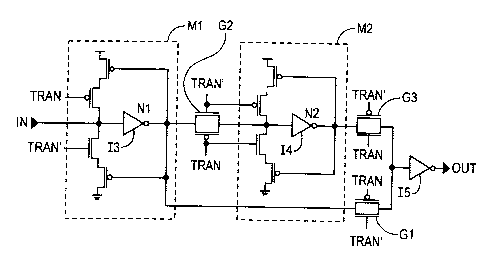
[00013 Figure 1 B illustrates the portion of the exemplary receiver that
locally stores a signal indicative of the "next" digital state to be output by
the
receiver. This portion of the receiver primarily includes two tri-state
inverters
M1 and M2 and transmission gates G 1, G2, and G3. As in Figure 1 A, the
input signal, IN, is received from the interconnect line and is provided to
tri-
state inverter M1. The output of tri-state inverter M1 is provided as an input
signal to tri-state inverter M2 through transmission gate G2 and as an input
to
transmission gate G1. The output of tri-state inverter M2 is provided to
transmission gate G3. Control signals TRAN and TRAN' enable and disable,
depending upon the states of TRAN and TRAN', the transmission gates G'1,
G2 and G3 and tri-state inverters M1 and M2. The outputs of transmission
gates G1 and G3 are multiplexed and alternatively passed through inverter 15.
The output of inverter 15 comprises the output signal of the receiver circuit,
OUT, which is provided as input to the next electrical component on the chip.
As explained in more detail below, node N1 (at the output of inverter 13)
holds
the complementary state to the present state on the interconnect line (i.e.,
input signal IN). Node N2 (at the output of inverter 14) holds the current
state
on the interconnect line (i.e., input signal IN). The signal state at Node N1
is
provided through inverter 15 when the interconnect line is quiet to generate
output signal OUT, which matches the state on the interconnect line (i.e.,
input signal IN). When a transition of the input signal IN is detected, the
signal state at Node N2 is provided through inverter 15 to generate output
signal OUT, which is the complement to the previous state of output signal
OUT. Thus, the signal held at node N2 is directly used to generate the
complement to the current output signal OUT, i.e., the signal at node N2 is
CA 02422208 2003-03-14
indicative of the complement of output signal OUT. Transmission gates G1
and G3 together act as a multiplexer for the input signal (from Node N1 and
Node N2) to inverter i5, which ultimately generates output signal OUT.
[00014] Now, with continuing reference to Figures 1A, 1 B and with
reference to Figures 2 and 3, operation of the exemplary receiver will be
described. Figure 2 illustrates a portion of an exemplary data pulse train on
an interconnect line on an integrated chip, the end of which being connected
to the exemplary receiver described herein. Figure 3 illustrates the output of
the exemplary receiver in response to the data pulse train in Figure 2 as
input
to the receiver. By way of example, assume that the state on the interconnect
line begins as "low" or "0", as illustrated on the far left side of Figure 2.
At this
point, because there is no transition occurring, the output of the XOR gate
(Figure 1 A) is "0", and thus the TRAN signal is "0" and TRAN' is "1 ". As a
result, transmission gates G1 and G2 are open, and transmission gate G3 is
closed, thereby causing the input signal to inverter 15 to have the state at
node N1 (at the output of inverter 13), which is the complement to the state
on
the interconnect line. Therefore, the output signal OUT is the same state as
the state on the interconnect line (i.e., input signal IN). Thus, as shown in
Figure 3, the output signal OUT is "low" or "0" when the input signal IN is
"low"
or "0". The output signal, OUT, of the receiver is held by the signal state on
the interconnect line (i.e., input signal iN) because there is no signal
transition
occurring on the interconnect line. Node N2 is holding the complementary
state of Node N 1, i.e., "high" or "1 ", since tri-state inverter M 1 and
transmission gate G2 are enabled. Further, node N2 is isolated from the
output terminal of the receiver because transmission gate G3 is disabled.
6
CA 02422208 2003-03-14
[00015] When the state on the interconnect line begins to transition to a
"high" or "1" level, the inverter T1 or T2 (in Figure 1A) skewed toward the
lower signal threshold changes state when the signal height on the
interconnect line passes the lower threshold. Consequently, the output of the
XOR gate changes to "1", and thus the TRAN signal becomes "1" and TRAN'
becomes "0", indicating that a signal transition has been detected. With
TRAN being "1" and TRAN' being "0", transmission gate G1 closes and
transmission gate G3 opens, thereby causing the input signal to inverter 15 to
take on the value of node N2, which is holding the complementary signal state
to node N1. Therefore, the output signal OUT changes from "0" to "1". In this
way, the output signal, OUT, takes on the next signal state when a signal
transition is detected on the interconnect line without having to wait for the
entire interconnect line to be driven high enough to drive the next electrical
component in the circuit. Further, with the TRAN signal being "1" and TRAN'
being "0", tri-state inverter M1 is disabled and transmission gate G2 is off.
Therefore, the signal at node N2 is isolated from and unaffected by the
changing signal on the interconnect line (i.e., input signal iN). Thus, the
output signal OUT continues to reflect the signal held at N2 until the
transition
of the signal on the interconnect line (i.e., input signal IN) reaches the
high
signal threshold.
[00016] When the transition of the signal on the interconnect line (i.e.,
input signal IN) reaches the high signal threshold, the second skewed inverter
T1 or T2 (Figure 1 A) detects the transition of input signal IN on the
interconnect line, and thus changes state such that the outputs of both T1 and
T2 are the same. Consequently, the output of XOR gate goes back to "0",
CA 02422208 2003-03-14
and therefore, the TRAN signal becomes "0" and TRAN' becomes "1". When
TRAN becomes "0" and TRAN' becomes "1", transmission gate G1 opens and
transmission gate G3 closes. Consequently, the state at Node N1 is passed
through inverter 15 to generate output signal OUT, which is the same as the
state on the interconnect line (i.e., input signal IN). Additionally, tri-
state
inverter M2 is disabled, tri-state inverter M1 is enabled, and transmission
gate
G2 is turned on. As a result, the state at node N2 changes to the
complementary state of the state at node N1. Again, because transmission
gate G3 is "off", the signal state at node N2 (complementary to the state at
Node N1) is isolated from and does not affect the output signal OUT. Thus,
the signal state at node N2 (complementary to the state at Node N1 ) is stored
until the next transition of the signal on the interconnect line is detected.
The
above-described operation is repeated when the signal on the interconnect
line (i.e., input signal IN) begins its next transition.
(0001' The exemplary receiver described hereinabove is advantageous
because, by essentially anticipating the signal level at the end of a
transition
on an interconnect line (by holding the next state locally), the receiver
increases the signal propagation performance on the interconnect line with
less need for repeaters interposed throughout the interconnect line. The
decreased need for repeaters on the integrated chip frees up physical space
on the chip. Furthermore, the elimination of a number of repeaters from the
chip decreases the overall power consumption of the chip. One skilled in the
art will recognize other benefits of the exemplary receiver disclosed above.
(00018] While the invention has been described in reference to a
s
CA 02422208 2003-03-14
particular embodiment thereof, the invention may be embodied in other
specific forms without departing from its spirit or essential characteristics.
By
way of example only, one skilled in the art will recognize many equivalent
structures and devices for storing the next state of the interconnect line,
such
as flip flop circuits, memory devices, etc. Further, one skilled in the art
will
recognize many equivalent structures and devices for detecting the transition
on an interconnect line. Accordingly, the described embodiment is to be
considered in all respects only as illustrative and not restrictive, The scope
of
the invention is, therefore, indicated by the appended claims rather than by
the foregoing description. All changes that come within the meaning and
range of equivalency of the claims are to be embraced within their scope.
9