Note: Descriptions are shown in the official language in which they were submitted.
CA 02422572 2003-03-14
WO 02/25334 PCT/GBO1/04191
1
ISOLATION DEVICE BETWEEN OPTICALLY CONDUCTIVE AREAS
TECHNICAL FIELD
This invention relates to an isolation device for providing optical and
electrical
isolation between areas of an integrated optical circuit.
BACKGROUND PRIOR ART
It is known to isolate two optically conductive areas of an integrated optical
circuit
from each other by providing a trench between the two areas. If the trench is
empty,
optical isolation is provided by reflection of stray light at the interFace
between the
optically conductive area and the trench. It is preferable instead to absorb
the stray
light by filling the trench with light absorbent material. However, this may
have a
tendency of reducing the electrical isolation between the two optically
conductive
areas.
It is also known to absorb stray light by providing dopant in selected areas
of an
optical chip, e.g. as described in WO-A-99/28772, the disclosure of which is
incorporated herein.
This invention aims to provide an alternative form of device, which provides
both
optical and electrical isolation.
SUMMARY OF THE INVENTION
According to the invention, there is provided an isolation device for
providing optical
and electrical isolation between two optically conductive areas of an
integrated
CA 02422572 2003-03-14
WO 02/25334 PCT/GBO1/04191
2
optical chip comprising a first elongate region extending across the chip
doped with a
first dopant material, a second elongate region extending across the chip on
one
side of the first elongate region and a third elongate region extending across
the chip
on the opposite side of the first elongate region, the second and third
elongate
regions being doped with a second dopant material of opposite polarity to the
first
dopant material so a first diode is formed between the second and first
elongate
regions and a second diode is formed between the first and third elongate
regions,
the first and second diodes being connected in series with opposing polarity.
Preferred and optional features of the invention will be apparent from the
following
description and from the subsidiary claims of the specification.
BRIEF DESCRIPTION OF DRAWINGS
The invention will now be further described, merely by way of example, with
reference to the accompanying drawings, in which: -
Figure 1 is a schematic cross-sectional view through a device according to one
embodiment of the invention;
Figure ~ is a schematic cross-sectional view through a device according to
another
embodiment of the invention; and
Figure 3 is a schematic plan view of a variable optical attenuator
incorporating
devices such as shown in Figures 1 and 2; and
Figure 4 is a schematic cross-sectional view through a device according to a
further
embodiment of the invention.
CA 02422572 2003-03-14
WO 02/25334 PCT/GBO1/04191
3
BEST MODE OF THE INVENTION
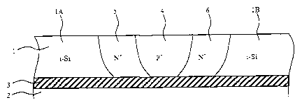
Figures 1 and 2 show devices comprising an n-p-n junction formed in the
silicon
layer of a silicon-on-insulator (SOI) chip comprises a layer of silicon 1,
separated
from a substrate 2 (which may also be of silicon) by an insulating layer 3,
e.g. of
silicon dioxide.
The silicon layer 1 is nominally intrinsic, i.e. with no n or p doping,
although in
practice it tends to contain a very small amount of p-dopant. Figure 1 shows
first
and second areas 1A and 1B of the silicon layer 1 which are separated by an n-
p-n
junction comprising an elongate p-doped region 4, a first elongate n-doped
region 5
on one side thereof and a second elongate p-doped region 6 on the opposite
side
thereof. The regions 4 and 5 thus form a first pn junction and the regions 4
and 6
form a second pn junction, the two pn junctions being connected in series (by
the
common p-doped region 4) with opposing polarity. It will be appreciated that
current
may flow through a forward biased pn junction but not through a reverse biased
pn
junction. Thus, even if an electrical potential exists between the first area
1A and the
second area 1 B, no current can flow therebetween through the regions 4, 5 and
6 as
this potential will reverse bias one of the pn junctions. The n-p-n junction
thus
electrically isolates the first area 1A from the second area 1B. Furthermore,
the
dopant provided within the regions 4, 5 and 6 absorbs stray light attempting
to pass
either from area 1A to area 1 B or vice versa. The n-p-n junction thus also
effectively
optically isolates the area 1 A from the area 1 B.
As shown in Figure 1, the p-doped region 4 and the n-doped regions 5 and 6
preferably extend down to the oxide layer 3 (which is electrically non-
conductive) so
there is no undoped silicon path extending from area 1A to area 1 B.
CA 02422572 2003-03-14
WO 02/25334 PCT/GBO1/04191
4
The doped regions 4, 5 and 6 may be fabricated by a variety of known methods
involving ion implantation and/or diffusing in of dopant and may take forms
other
than those shown in Figure 1. Each of the n-doped regions 5 and 6 is shown
contiguous with the p-doped region 4 so there is no undoped silicon area
therebetween. Alternatively, the adjacent regions may overlap to some extent
(as
shown in Figure 2). Such arrangements are suitable where the applied voltage
is
relatively low, e.g. 5V, and a compact layout is required.
Figure 2 shows an alternative form of device in which a trench 7 is first
etched in the
silicon layer 1 prior to formation of the n-p-n junctions. The layer of
silicon remaining
at the base of the trench 7 is thus shallower so making it easier to form the
doped
regions 4, 5 and 6 through to the oxide layer 3.
Figure 2 shows a thin silicon layer remaining beneath the doped regions 4, 5
and 6
but, as indicated above, the doped regions 4, 5 and 6 preferably extend
through the
entire depth of the silicon layer to the oxide layer 3.
In a typical SOI chip, the silicon layer 1 may have a thickness (from the
surface of
the chip to the oxide layer 3) of 4 - 8 microns. The trench 7 is preferably
etched to a
depth such as to leave a layer of silicon at the base thereof of a thickness
of around
2.6 microns.
The trench 7 may be etched deeper, or a further trench etched at the base
thereof,
to reduce the thickness of silicon remaining further so long as the remaining
layer of
silicon has a sufficient thickness to enable the doped regions 4, 5 and 6 to
be formed
therein. However, in practice, the trench may be formed at the same time as
other
etched features on the chip, e.g. p-i-n diodes (see below), so will be subject
to the
minimum thickness requirements of these features, which might typically be 1
micron.
CA 02422572 2003-03-14
WO 02/25334 PCT/GBO1/04191
The depth of the trench 7, or the thickness of the silicon layer, in which the
n-p-n
junction is formed, need not be uniform across the device.
An isolation device such as that described above, may be used to provide
optical
and electrical isolation between selected components of an integrated optical
circuit.
In particular, it may be used between adjacent optical waveguides. For
instance, a
variable optical attenuator (VOA) may comprise 40 or more channels and
comprise
an array of rib waveguides formed in the silicon layer spaced from each other
at a
pitch of about 250 microns. Figure 3 shows a plan view of part of such a VOA
comprising a plurality of rib waveguides 8 extending across a chip 9. Tapered
sections 8A are provided at each end of the waveguides to facilitate a low
loss
coupling with an optical fibre (not shown). The tapered sections 8A may, for
instance, be as described in US6108478. Attenuation devices 10 are provided on
each waveguide 8 to provide variable attenuation of the optical signal carried
by the
waveguide 8. The attenuation device may, for instance, comprise one or more p-
i-n
diode modulators, e.g. as described in US5757986 or co-pending application No
GB0019771.5 (Publication No .....................). Isolation devices 11
comprising n-
p-n junctions as described above are provided between each pair of waveguides
8 to
provide electrical and optical isolation between adjacent waveguides and their
associated attenuation devices 10. The devices are shown as comprising n-doped
regions 11A each side of a p-doped region 11B as described in relation to
Figures 1
and 2.
In a further embodiment, especially where the electrical isolation to high
voltages is
required, e.g., in excess of 90V, the p-type and n-type regions are preferably
separated by a relatively undoped or intrinsic region. Figure 4 shows such a
form of
device in which a trench 7A is first etched in the silicon layer 1, prior to
formation of n
and p-type regions, 5A, 6A and 4A, separated by intrinsic regions 12 so as to
form a
n-i-p-i-n junction. As previously indicated, the n and p-type doped regions
preferably
extend through the entire depth of the silicon layer to the oxide layer 3 to
prevent any
CA 02422572 2003-03-14
WO 02/25334 PCT/GBO1/04191
6
current leakage across the junction between the regions 1A and 1 B. The n-i-p-
i-n
arrangement provides better reverse breakdown characteristics due to the less
steep
doping concentration gradient between the p and n-doped regions, due to the
intrinsic regions 12 therebetween.
Figure 4 also shows a cross-section through a p-i-n diode attenuator device
10, such
as that described above, on one side of the n-i-p-i-n junction.
The provision of an isolation device such as that described above between
adjacent
waveguides can significantly reduce the cross-talk between the channels caused
either by stray light passing from one waveguide to another or electrical
signals
applied to an attenuator 10 on one waveguide affecting the attenuators 10 on
adjacent waveguides.
A device such as that shown in Figure 1, Figure 2 or Figure 4, may, typically,
have a
width (i.e. the width of the n-p-n (or n-i-p-i-n) junction) in the range 20
microns to 50
microns. The n-p-n (or n-i-p-i-n) junction is formed by the elongate regions
4, 5 and
6 which extend a required distance across the optical device. In the example
of a
VOA mentioned above, they may, for instance, extend the entire length of the
chip
(as shown in Fig 3), which may be a distance 20 mm or more.
It will be appreciated that a similar n-p-n (or n-i-p-i-n) junction may be
formed in other
types of chip to optically and electrically isolate one are from another, e.g.
a IIIN
material system or other semiconductor material.
A p-n-p (or p-i-n-i-p) junction may be used in place of the n-p-n (or n-i-p-i-
n) junctions
described. if the nominally intrinsic silicon layer 1 were slightly n-doped,
this would
be preferred.
CA 02422572 2003-03-14
WO 02/25334 PCT/GBO1/04191
7
The p-type dopant may typically comprise boron provided at a dopant level of
at
least 10~$ cm'3, e.g., in the range of 10~$ to 102° cm'3, or higher.
The n-type dopant may typically comprise phosphorous provided at a dopant
level of
at least 10~$ cm'3, e.g., in the range of 10~$ to 102° cm'3, or higher.
The dopant concentrations are preferably substantially uniform along the
length of
the elongate doped regions although, in practice, some variations may occur.