Note: Descriptions are shown in the official language in which they were submitted.
CA 02422624 2003-03-17
DESCRIPTION
SEMICONDUCTOR BASE MATERIAL AND METHOD OF MANUFACTURING
THE MATERIAL
Technical Field
s The present invention relates to a semiconductor base
and a production method thereof. More particularly, this
invention relates to a structure useful when using a
semiconductor material associated with easy occurrence of
dislocation defects and a method thereof.
to Background Art
For crystal growth of a GaN group material, a substrate
that does not lattice match therewith, such as sapphire, SiC,
Spinel, and recently Si and the like, has been used due to the
absence of a substrate that lattice matches with GaN group
Is materials. However, a GaN film produced contains dislocations
of as many as 101° points/cmz due to the absence of lattice
match. While high luminance Light Emitting Diodes,
semiconductor lasers and the like have been realized in recent
years, reduction of dislocation density has been desired for
Zo improved properties.
As a method for reducing the dislocation density when,
for example, a GaN group semiconductor substrate and the like
are grown on a buffer layer and a GaN substrate by vapor phase
growth, a method comprising formation of a partial mask on the
2s aforementioned substrate and selective growth to achieve
crystal growth in the lateral direction has been proposed,
thereby to give a high quality crystal having a reduced
dislocation density (e. g., JP-A-10-312971).
It has been clarified that, according to the above-
3o mentioned method, a problem occurs that, in the part of a mask
layer where growth in the lateral direction occurred, the C
axis tilts in a slight amount toward the direction of the
lateral growth, which in turn causes a new problem of degraded
crystal quality (Abstracts G3.1 of MRS 1998 Fall Meeting).
1
CA 02422624 2003-03-17
This can be confirmed through measurement (~ scan) of the
incident orientation dependency in X-ray rocking curve
measurement (XRC). That is, a full width at half-maximum
(FWHM) of X-ray rocking curve by incident X-ray from the
direction of lateral growth is greater than the FWHM value by
X-ray from a stripe direction of a mask layer, which means the
presence of orientation dependency in the micro tilting of the
C axis. This suggests a possibility of inducing a number of
new defects in the junction part of the lateral growth on the
mask.
As the mask layer material, Sioz is generally used.
However, a problem has been found that, when a crystal growth
layer is laminated thereon, the Si component transfers into
the crystal growth layer, constituting a problem of autodoping
is contamination.
When a semiconductor material containing A1, such as
AlGaN, is grown on a substrate having an Si02 mask layer,
crystal growth occurs on the mask layer, too, preventing
effective selective growth itself.
2o In an attempt to solve such problems, a method has been
proposed wherein a stripe groove processing is applied to a
substrate having a buffer layer and a GaN layer formed on an
SiC base substrate, which groove reaching the SiC layer to
form a convex, and crystal growth is started from the GaN
as layer on the top of this convex (Abstracts 63.38 of MRS 1998
Fall Meeting). According to this method, a selective growth
without an Sio2 mask layer is possible, whereby resolving
various problems caused by the use of the aforementioned Si02
mask.
3o For the above-mentioned method, a sapphire substrate can
be used as the base substrate and the method thereof is also
disclosed (e. g., JP-A-11-191659). The above-mentioned method
requires steps of crystal growing a buffer layer material and
a GaN group material on a sapphire base substrate, taking the
35 substrate out from a growth furnace to apply a groove
2
CA 02422624 2003-03-17
processing, and then crystal growing again, thus posing a new
inconvenience of complicated production process, increased
number of steps, higher cost and the like.
In addition, a method for suppressing propagation of
dislocation by forming concavo-convex grooves on a substrate
and growing a gallium nitride group semiconductor while
forming a cavity in the concave part has been disclosed (JP-A-
2000-106455). According to this method, a low dislocation
density area can be formed by a single growth, but a cavity
1~ needs to be fornned. Thus, when a light emitting element and
the like are prepared, it is inconvenient when releasing the
heat generated in the light emitting part to the substrate
side, thus problematically encouraging thermal degradation of
laser diode and the like. Moreover, since this method does not
i5 actively control propagation of dislocation, the dislocation
propagates to the upper part of the convex part,
problematically making reduction of dislocation density
insufficient.
3
CA 02422624 2003-03-17
Disclosure of the Invention
In view of the above-mentioned problems, it is therefore
an object of the present invention to avoid various problems
caused by the use of a mask layer, and to simplify the
production step. The invention additionally aims at resolving
the problem of unattainable selective growth of AlGaN, which
1° has been conventionally difficult. Moreover, the invention
aims at avoiding the issue of heat caused by the formation of
cavity parts.
The semiconductor base of the present invention consists
of a substrate and a semiconductor crystal formed on the
is substrate by vapor phase growth, wherein said substrate is a
crystal substrate comprising sapphire, SiC, Si, Spiel, ZnO,
GaAs or NGO and has a crystal growth plane having a concavo-
convex surface, and the aforementioned semiconductor crystal
is an AlXGa1_X_yInyN ( Osx5l, Osysl, Osx+ysl ) crystal grown from
Zo the concave part and/or the convex part while forming a facet
structure.
It is preferable to make the convex part of the crystal
growth plane of the above-mentioned substrate a convex part
having a parallel stripe pattern. It is more preferable that
Zs the above-mentioned semiconductor crystal be InGaAIN (i.e.,
AlxGa1_X_yInyN) and the longitudinal direction of the stripe be
parallel to the (1-100) plane or the (11-20) plane of the
InGaAIN crystal.
In a stripe structure obtained by subjecting the above-
3o mentioned substrate to concavo-convex processing, it is
desirable that the longitudinal direction of the stripe be
parallel with the (1-100) plane or the (11-20) plane of the
above-mentioned InGaAIN crystal and the precision thereof be
not more than 1°. In a preferable stripe structure, the total
3Q
CA 02422624 2003-03-17
(A+B) of width A of the convex part and width B of the
adjacent concave part is not more than 20 E,~n, and a depth H of
the aforementioned concave part is not less than 20% of the
greater width of A or B.
It is also desirable to make an angle formed by the
rising slope of a convex part formed by concavo-convex
processing of the above-mentioned substrate, and a substrate
plane to be not smaller than 60°. It is also possible to equip
a curved part on the bottom of the concave part.
In the above-mentioned semiconductor base, the crystal
growth plane of the aforementioned substrate may be a concavo-
convex surface, wherein the concave plane of the concavo-
convex surface is processed such that crystal growth does not
occur substantially from the surface thereof, and a
is semiconductor crystal may be grown from the convex part while
forming a facet structure.
CA 02422624 2003-03-17
30 Brief Description of the Drawing
Figure 1 is a cross section for explanation of the state
of crystal growth of the semiconductor base of the present
invention.
Figure 2 is a cross section for explanation of the state
3s of crystal growth of the semiconductor base of the present
4a.
CA 02422624 2003-03-17
invention.
Figure 3 is a cross section for explanation of the state
of crystal growth of the semiconductor base of the present
invention.
Figure 4 is a cross sectional photograph showing
complete formation of facets.
Figure 5 is a cross sectional photograph showing
incomplete formation of facets.
Figure 6 is a cross sectional photograph showing bending
to of the dislocation line (black line in the photograph) along
with the growth of the facet.
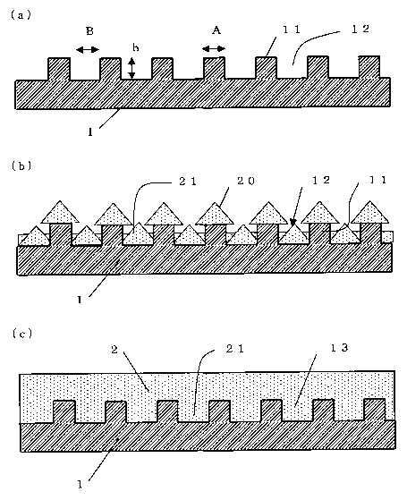
In each of the Figures, 1 is a substrate, 11 is a convex
part, 12 is a concave part, 13 is a cavity part and 2 is a
semiconductor layer.
is Detailed Description of the Invention
The present invention is characterized in that a
concavo-convex surface is formed on a substrate before
formation of even a buffer layer and the like, thereby to
provide a base surface, on which a facet plane can be formed,
2o from the start of crystal growth. That is, by equipping a
concavo-convex surface on the substrate, each or both of the
concave plane and the convex plane separated by steps is/are
prepared as unit standard surface on which to grow a facet
structure in vapor phase growth. When both the concave plane
zs and the convex plane are prepared as planes capable of facet
structure growth, the crystal growth occurs in the entirety of
the substrate surface in the initial stage of the growth, thus
resulting in the growth comprising a facet plane on both the
convex part and the concave part. In contrast, when either the
3o concave plane or the convex plane is substantially incapable
of crystal growth because it has an extremely small width and
the like, or the crystal growth itself is possible but the
surface thereof is processed and substantially incapable of
crystal growth, the facet structure growth occurs from either
3s the convex part or the concave part. In some cases, the facet
CA 02422624 2003-03-17
structure growth occurs from either the convex part or concave
part but non-facet structure growth occurs from the other
plane.
As a result, the dislocation line extending from the
substrate in the C axis direction is bent toward the lateral
direction in the facet plane and fails to propagate upward.
Subsequent continuous growth makes the growth plane flat in
time and the vicinity of the surface thereof becomes a low
dislocation density area due to the absence of propagation of
to dislocation from the substrate. In other words, the formation
of a low dislocation density area is achieved without using a
mask layer as in conventional cases and without necessitating
a grounding layer. Particularly, the problem of heat
dissipation can be avoided due to the absence of the need to
i5 form a cavity part.
The embodiment of the present invention is explained in
detail in the following based on drawings.
Figures 1(a) to 1(c) show cross sectional views to
explain the state of crystal growth of the semiconductor base
20 of the present invention. In these Figures, 1 is a substrate
and 2 is a semiconductor crystal grown by vapor phase growth
on the substrate 1. On the crystal growth plane of the
substrate 1 are formed a convex part 11 and a concave part 12,
which are the base surfaces on which to form a facet plane
2s from the aforementioned convex part 11 and/or concave part 12.
The above-mentioned substrate 1 is a base substrate on
which to grow various semiconductor crystal layers, in the
state before the formation of a buffer layer and the like for
lattice matching. As such substrate, sapphire (C-plane, A-
3o plane, R-plane), SiC (6H, 4H, 3C), GaN, A1N, Si, Spinel, ZnO,
GaAs, NGO and the like can be used, but other materials may be
used as long as the object of the invention is achieved. The
plane, direction of the substrate is not particularly limited
and may be a just substrate or one having an off angle. In
3s addition, a sapphire substrate and the like having several ~n
6
CA 02422624 2003-03-17
of GaN group semiconductor epitaxially grown thereon may be
used.
As the semiconductor layer to be grown on the substrate
1, various semiconductor materials can be used. Examples
thereof include AlXGa1_X_ylnyN ( Osxsl, Osysl, 05x+y~l ) wherein
the composition ratios of x and y are varied, such as GaN,
Alo.2Gao.eN, Ino.4Gap.6N and the like.
In the case of a semiconductor material containing Al,
such as AlGaN and the like, the conventional mask method poses
1o a problem of growth on an Si02 mask layer. Because the present
invention resolves this problem by eliminating masking,
conventionally unattainable AlGaN low dislocation density can
be now achieved, whereby a low dislocation, high quality film
growth is afforded from right above the substrate. As a
Is result, light absorption by GaN layer, a problem in
ultraviolet light emitting element and the like, is
obliterated, which is particularly preferable from a practical
aspect.
The following explains a base surface capable of forming
ao a facet plane, wherein concavo-convex shaped parts 11 and 12
are formed on a crystal growth plane of substrate 1.
For typical growth of GaN, a high temperature GaN film
is grown on a sapphire C-plane substrate via a low temperature
buffer layer by conventional MOVPE method and the like. When a
z5 high temperature GaN is grown on a low temperature buffer
layer, the buffer layer becomes a core, which core joins along
with the growth in the lateral direction and becomes flat. At
this point, because the sapphire substrate is free of
processing, the growth proceeds to form a stable C-plane and
3o GaN becomes flat. This is attributable to the fact that the
growth rate in the lateral direction is faster than that of
the stable C-plane.
On the other hand, when the rate of growth in the
lateral direction is suppressed and the rate of growth in the
3s C axis direction is increased, an inclined facet .(1-101} and
7
CA 02422624 2003-03-17
the like can be formed. In the present invention, the growth
plane of the substrate is subjected to a concavo-convex
processing to suppress the above-mentioned growth in the
lateral direction.
In the present invention, the shape of the concavo-
convex is subject to no particular limitation as long as the
above-mentioned effect can be achieved, and various shapes can
be employed.
For forming such a concavo-convex surface, island type
so intersperse convex parts, stripe type convex parts consisting
of convex lines, lattice convex parts, convex parts wherein
the lines farming these are curves and the like, can be
employed.
Of these modes of the convex part, one comprising a
15 stripe convex line is preferable, because the production steps
thereof can be simplified and regular patterns can be easily
formed. While the longitudinal direction of the stripe may be
any, when the material to be grown on the substrate is GaN and
said direction is the <11-20> direction of the GaN group
zo material, the growth in the lateral direction can be
suppressed and oblique ~1-101} facets and the like are easily
formed. As a result, the dislocation propagated in the C axis
direction from the substrate side is bent in this facet plane
to the lateral direction and resists upward propagation, which
Zs in turn particularly preferably forms a low dislocation
density area.
Even when the stripe direction is set for the <1-100>
direction, similar effects as mentioned above can be obtained
by determining the growth conditions permitting easy formation
30 of facet plane.
The direction of the stripe forn~ed by concavo-convex
processing of the above-mentioned substrate is most preferably
the <1-100> direction or the <11-20> direction of the InGaAIN
crystal. However, because it accompanies a growth phenomenon
3s where adjacent facets are joined and leveled, the direction
s
CA 02422624 2003-03-17
may not match strictly the aforementioned direction. While the
presence of a little direction error is tolerable, it is
desirable to make the precision of the stripe direction of not
more than 1°, particularly preferably within 0.2°, relative to
the <1-100> direction or the <11-20> direction of InGaAIN
crystal.
In Fig. 1, as shown in (a), substrate 1 wherein width B
of a concave part 11 and width A of the convex part 12 are the
same, is used. In this case, the growth proceeds while forming
1° facet planes in both the convex part 11 and the concave part
12, thereby forming crystal units 20 and 21. Because, in
concave part 12, the growth occurs in the valley between the
sidewall and the facet plane, as shown in Fig. 1(b), a buried
valley is included. When the crystal growth continues in this
15 situation, the crystal unit 21 on the convex part 11 and the
crystal unit 21 on the concave part grow, films are joined and
the concavo-convex surface of substrate 1 is covered as shown
in Fig. 1(c). In this case, a low dislocation area is formed
on the upper part where a facet plane was once formed, and the
zo produced film comes to have high quality.
In the embodiment of Fig. 2, as shown in (a), a
substrate 1 wherein width A of convex part 11 is narrower than
width B of concave part is used. In this case, the growth
proceeds in the convex part 11 forming a facet plane, and
Zs crystal growth occurs in the concave part 12 as well (Fig.
2(b)). In this situation, when the crystal growth continues,
v
the films grown from the convex part 11 and the concave part
12 are joined to cover the concavo-convex surface, as shown in
Fig. 2(c). In this case, while a low dislocation area is
ao formed on the upper part 11 where a facet plane was once
formed, but a facet plane is difficult to form from the shape
of the concave part 11, and the effect of bending the
dislocation to the lateral direction reduces. Thus, as
compared to the embodiment of Fig. 1, while the effect of
3s reduction of dislocation density is small, the produced film
9
CA 02422624 2003-03-17
comes to have high quality.
While the area where a facet plane is formed varies
greatly by the combination of width B of the concave part and
width A of the convex part, propagation of dislocation can be
bent by the formation of facet planes, whereby low dislocation
density can be achieved. Accordingly, while this facet plane
may be any as long as the propagation of dislocation is bent,
in a preferable embodiment as shown in Fig. 1, crystal unit 20
grown from ane facet structure growth base plane does not have
I° a flat part on its top plane but has an angle shape where both
facet planes completely cross at the top part (Fig. 4 shows
complete formation of facet and Fig. 5 shows cross sectional
photograph showing an incomplete case). Such facet plane shown
in Fig. 1 (Fig. 4) is preferable because it can bend almost
Is all the dislocation lines succeeded from the aforementioned
base plane and can further reduce the dislocation density
right above. Fig. 6 is a cross sectional photograph showing
such state, wherein it is clearly observed that the
dislocation line (black line in the photograph) is bent along
Zo the facet growth.
The area where the facet plane is formed can be
controlled by not only the combination of width but by
changing the depth h of the concave part (height of convex
part).
25 As mentioned above, the combination of concavo-convex
includes various ones. In view of the application to a light
emitting element, the width of concave Bart 12 and convex part
11, and the depth h of the concave part are preferably such
that the total (A+B) of width A of the convex part and width B
30 of the adjacent concave part is not more than 20 Vin, and the
depth h of the aforementioned concave part is not less than
20~ of the greater width of A or B.
When the facet plane to be formed is {1-101} facet, the
angle of the facet plane thereof with the substrate plane is
3s about 60°. Therefore, the height necessary for complete
CA 02422624 2003-03-17
formation of the facet in this case is J3/2 (i.e., (square root
of 3)/2) relative to the width of the bottom surface. When the
bottom surface is considered to correspond to width B of
concave part or width A of convex part, forming the facets, A
should have the height of B x x/3/2. When A or B exceeds 20 ~,m,
the necessary height is about 17 ~ln, frequently posing the
problems of occurrence of warp due to a thick substrate, long
,time for growth and the like. As a result of the studies of
the~present inventors, when A+B520 Vin, occurrence of warp could
to be reduced and the growth did not require a long time.
The depth h of the concave part has been also considered
in the same manner as above, and it has been confirmed that
when it is set for not less than 20% of the longer of A or B,
the facets are formed and reduction of dislocation can be
15 promoted.
The angle formed by the rising slope of a convex part 11
formed by concavo-convex processing of the substrate, and a
substrate plane is preferably not smaller than 60°,
particularly desirably as near as possible to a right angle.
so ~nThen it is smaller than 60°, the growth begins from the slope
of the convex part and a problem of difficult flattening after
facet growth occurred. As a result of the studies of the
present inventors, it has been found that an angle of not less
than 60°, among others a rising slope near a right angle,
2s pewits formation of facets and flattening thereafter is not
substantially inhibited. If possible, a slope angle exceeding
90° is also preferable.
It is also possible to provide a curve on the bottom
surface of concave part 12 concavo-convex processed on the
3o substrate. Typically, a curve having a gentle concave surface
when seen at a cross section between the rising base of one
convex part 11 and the rising base of the adjacent convex part
11. When such curve is provided, the growth can be controlled
such that the growth from the concave part 12 becomes slow and
35 the growth from the convex part 11 is dominant.
1l
CA 02422624 2003-03-17
Fig. 3 shows another embodiment of the present
invention. The formation of concavo-convex and the like are as
shown in Fig. 1, but as shown in Fig. 3(a), in this
embodiment, a mask layer 3 is formed on the concave part 12 of
the substrate 1, which prevents substantial crystal grow from
the surface. In this case, the growth while forming a facet
plane occurs only from the convex part 11, crystal unit 20 is
formed (Fig. 3(b)), and when the crystal growth is continued,
crystal units 20 grown from each convex part 11 are joined to
to cover the concavo-convex surface as shown in Fig. 3(c). In
this embodiment, too, when the facet plane is formed, the
propagation of dislocation can be bent, thereby low
dislocation density can be achieved.
In the above-mentioned embodiment, as the mask layer 3,
is an Si02 mask and the like can be used. The processing is free
of any particular limitation as long as it prevents
substantial crystal growth, such as formation of a thin film
and the like. In addition, by making either the concave part
or the convex part a concave part having a minute opening or a
ao convex part having a minute width that cannot cause
substantial crystal growth, the growth of the facet structure
can be made to occur from only one of them.
In the above, an embodiment where only a single layer of
the semiconductor layer 2 is grown on the substrate 1 has been
2s explained. To further reduce dislocation defects, a similar
steg may be repeated. Furthermore, similar steps may be
repeated to form plural semiconductor layers in multiplicity.
This constitution can gradually reduce the dislocation which
is propagated as the layers are laminated.
ao A convex part can be formed by a conventional
photolithography technique, which comprises patterning
according to the shape of the convex part and applying etching
processing by RIE technique and the like.
As a method for crystal growth of a semiconductor layer
as on a substrate, HVPE, MOVPE, MBE and the like may be
12
CA 02422624 2003-03-17
performed. When a thick film is to be prepared, the HYPE
method is preferable, but when a thin film is to be prepared,
MOVPE method and MBE method are preferable.
Formation of the facet plane can be controlled by the
growth conditions (kind of gas, growth pressure, growth
temperature and the like) for crystal growth. In the case of
decompression growth, lower NH3 partial pressure leads to easy
formation of facets in the <1-101> plane and growth at normal
pressure leads to easy formation of facet planes as compared
so to reduced pressure.
When the growth temperature is raised, the growth in the
lateral direction is promoted, and the growth at a low
temperature causes more rapid growth in the C axis direction
than growth in the lateral direction, thereby making facet
Is plane easy to form.
The foregoing shows that the shape of facet can be
controlled by growth conditions. As long as the effect of the
present invention is afforded, other conditions can be
employed according to the object.
ao When the facet plane is formed and the dislocation is
bent in the lateral direction, the growth conditions are
preferably changed to promote growth in the lateral direction
to flatten GaN. To achieve this, the growth conditions under
which the facet plane is difficult to be formed can be
z5 employed, conversely from the aforementioned.
Examples
Example 1
A photoresist patterning (width: 2 Vin, period: 4 ~,am,
stripe direction: stripe extending direction is the <1-100>
3o direction of the sapphire substrate) was made on a C-plane
sapphire substrate and etched to a 2 ~,~m depth in a square
cross section with an RIE (Reactive Ion Etching) apparatus.
The aspect ratio then was 1. After removing the photoresist,
the substrate Was set on a MOVPE apparatus. Then, the
35 temperature was raised to 1100°C under a hydrogen atmosphere
13
CA 02422624 2003-03-17
and thermal etching was conducted. The temperature was lowered
to 500°C, and trimethyl gallium (hereinafter TMG) as a III-
group starting material and ammonia as an N starting material
were flown to grow a GaN low temperature buffer layer. Then,
the temperature was raised to 1000°C, and TMG and ammonia as
starting materials and silane as a dopant were flown to grow
an n-type GaN layer. The time for the growth was the time
corresponding to 2 E,,am of conventional GaN growth without
concavo-convex.
io Observation of cross section after growth revealed
growth in both convex part and concave part, as shown in Fig.
1(b).
Growth was performed according to a similar method for
the time corresponding to 6 ~,~m of conventional GaN growth free
is of concavo-convex. As a result, a flattened GaN film covering
the concavo-convex part was obtained.
For the measurement of dislocation density, the above-
mentioned sample was etched in a HZS04 : H3P04=1:1 ( 250°C )
solution for 90 min and the number of formed pits was counted.
2o In addition, the carrier density of the obtained film was
determined by Hall measurement. Furthermore, a full width at
half-maximum of X-ray rocking curve was also measured.
For comparison, a sample of growth on a sapphire
substrate free of concavo-convex processing and a sample
25 comprising 2 E,,am of GaN grown on a sapphire substrate free of
concavo-convex processing, an Si02 mask formed in the same
stripe direction and width as mentioned above and 4 ~,~m of GaN
grown on the substrate were prepared. The evaluation results
of each sample are shown in Table 1.
14
CA 02422624 2003-03-17
Table 1
sample dislocation carrier FWHM of XRC
density density (sec)
( Cm 2 ) ( Cm 3 )
Example 1 1x10 1X10 170
conventional 4X10' 5X101' 200 - 400
ELO
Normal GaN 2X10 ~ 1X10³ ~ 220
It is evident that the dislocation density was reduced
more in the sample of Example than in conventional ELO.
This is considered to be attributable to the occurrence
of bending of the penetrating dislocation also in the concave
part.
In contrast, the carrier density was of the same level
to as general GaN growth. The FWHM of XRC was 107 sec, which was
the smallest, and the film had high quality by general
evaluation.
Example 2
The procedure followed Example 1 except the shape of the
is concavo-convex part was changed to the following:.
(width: 2 ~"~n, period: 6 E,,~n, stripe direction: <1-100> of
sapphire substrate), and etched to the depth of 0.5 ',fin by RIE
apparatus in a square cross section.
Observation of cross section after growth revealed a
zo flattened film in which the concavo-convex part had been
buried as in Example 1, which is shown in Fig. 2(c). For
observation of dislocation density, pits were formed and the
number thereof was counted in the same manner as in Example 1.
Pits corresponding to the dislocation were scarcely
25 found on the upper part of the convex part. This is considered
to be the results of the growth that proceeded on the convex
part in the state where the facet plane had been formed, and
the dislocation was bent in the lateral direction.
Of the concave parts, those near the convex part did not
3o show very many pits, but a number of pits were found in the
CA 02422624 2003-03-17
area (width 4 E~m) near the center. This is considered to be
the results of dislocation propagated to the surface due to
the absence of facet plane near the center of concave part.
However, when the entire wafer is seen, it is clear that
dislocation density reduced as compared to the growth on the
substrate free of concavo-convex processing.
Example 3
The procedure followed Example 1 to grow GaN except an
Si02 mask was formed on the concave part. Observation of cross
io section of the film after growth corresponding to 2 ~m
revealed GaN grown with a facet plane formed on the upper part
of the convex part, as shown in Fig. 3(b). However, no film
was formed in the concave part.
Further growth resulted in the joining of the facets on
is the upper parts of the adjacent convex parts. Thereafter, the
growth proceeded to bury the joined valley part and a GaN film
was obtained in time having cavity on the upper part of the
concave part.
Pits were formed by etching. As a result, some pits
ao corresponding to the dislocation were confirmed to be present
in the center of the concave part. Except those, pits were
scarcely observed.
Example 4
An n-type AlGaN cladding layer, an InGaN light emitting
as layer, a p-type AlGaN cladding layer and a p-type GaN contact
layer were successively formed on the film obtained in Example
1 to give an ultraviolet LED wafer having a light emitting
wavelength of 370 nm.
Then, electrodes were formed and the element was
3o separated to give an LED element. The average output and
inverse current characteristic (leak current upon application
of -10V) of LED chips recovered from the whole wafer were
evaluated. For comparison, used were ultraviolet LED chips
wherein the above-mentioned structure was prepared by
3s conventional ELO technique and ultraviolet LED chips wherein
16
CA 02422624 2003-03-17
the above-mentioned structure was prepared using a
conventional sapphire substrate. The evaluation results of
these are shown in Table 2.
s Table 2
sample output (mW) leak current upon
(electric current application of -lOv
20 mA)
Example 4 1.7 10 (nA)
Conventional 1.5 50 (nA)
ELO
normal GaN 0.9 1 ( )
As shown in Table 2, the sample prepared according to
the present invention showed higher output as compared to the
I° conventional example, and it was found that a high quality LED
with less leak current could be prepared.
Example 5
The procedure followed Example 1 except that trimethyl
aluminum (TMA) was added when growing a semiconductor layer.
is As a result, a flat film of AlGaN (A1 composition 0.2)
was grown to cover the concavo-convex part. Pits were formed
by etching. As a result, there were not many pits
corresponding to the dislocation in the upper part of the
concave part. It was confirmed therefrom that an AlGaN film
2o could be made to have high quality (low dislocation density)
according to the present invention, which has not been
achieved by the conventional ELO technique.
Example 6
The following shows an embodiment using GaN as a
Zs substrate. A photoresist patterning (width: 2 ~,am, period: 4
~,am, stripe direction: <11-20> of GaN substrate) was made on a
GaN substrate and etched to a 2 ~n depth in a square cross
section with an RIE apparatus. After removing the photoresist,
the substrate was set on a MoVPE apparatus. Then, the
3o temperature was raised to 1000°C under a nitrogen, hydrogen,
17
CA 02422624 2003-03-17
ammonia mixture atmosphere. Thereafter, TMG - ammonia as a
starting material and silane as a dopant were flown to grow an
n-type GaN layer. The growth time then corresponded to 4 ~n of
conventional GaN growth free of concava-convex.
Observation of cross section after growth revealed a
flattened GaN film covering the concavo-convex part of the
substrate. Then, the pits in the obtained film were evaluated.
The pit density of GaN used as the substrate was 2x10⁶ cni2, but
growth in this Example resulted in the decrease in the number
io of pits, as evidenced by 1x106 cm 2 at the upper part of the
concave part, and 5x10⁴ ciri2 at the upper part of the convex
part. As such, it was confirmed that a further dislocation
density reduction effect was achieved in a substrate with less
dislocation.
is Example 7
Using the GaN crystal prepared in Example 1 as a first
crystal, a second crystal was grown thereon. A photoresist
patterning (width: 2 E,~m, period: 4 E,,~n, stripe direction: <11-
20> of GaN substrate) was made on the first GaN crystal and
Zo etched to a 2 ~,~n depth in a square cross section with an RIE
apparatus. The patterning was conducted such that the concave
part of the first crystal was disposed on the convex part of
the substrate. After removing the photoresist, the substrate
was set on a MOVPE apparatus. Then, the temperature was raised
25 to 1000°C under a nitrogen, hydrogen, ammonia mixture
atmosphere. Thereafter, TMG - ammonia as a starting material
and silane as a dopant were flown to grow an n-type GaN layer.
The growth time then corresponded to 4 ~n of conventional GaN
growth free of concavo-convex.
3o Observation of cross section after growth revealed a
flattened GaN film covering the concavo-convex part of the
substrate. Then, the pits in the obtained film were evaluated.
As a result, the number of pits decreased to 8x105 cm z. As
such, it was confirmed that a further dislocation density
3s reduction effect could be achieved by repeating this Example.
is
CA 02422624 2003-03-17
Industrial Applicability
According to the above-described semiconductor base of
the present invention and the production method thereof, a
base surface capable of forming a facet plane can be formed
s from the start of the crystal growth, without using a mask
layer, by applying a concavo-convex processing to the
substrate. Therefore, problems of occurrence of new defects in
the junction part of the part formed by lateral growth, due to
the micro tilting of the axis, autodoping and unavailable
io selective growth of A1-containing semiconductor materials,
which are due to the formation of a mask layer, can be
resolved. Furthermore, because the growth of from the growth
of a buffer layer to the growth of a semiconductor crystal
layer such as light emitting part and the like can be
is continuously conducted in a single growth after forming a
concavo-convex surface on a substrate, the production process
can be advantageously simplified. Particularly, due to the
absence of the need to form cavity parts, an additional effect
that the problem of heat dissipation can be avoided and the
zo like can be afforded, thereby making the invention highly
valuable for improvement of properties and reduction of cost.
This application is based on patent application Nos.
282047/2000 and 68067/2001 filed in Japan, the contents of
which are hereby incorporated by reference.
19