Note: Descriptions are shown in the official language in which they were submitted.
CA 02422794 2003-03-18
WO 02/25803 PCT/CA01/01338
COMPLEX VALUED DELTA SIGMA PHASE LOCKED LOOP
DEMODULATOR
Field of the Invention
The present invention relates to the
demodulation of frequency modulated (FM) signals and,
more specifically, it relates to a complex valued
delta sigma phase locked loop (PLL) demodulator.
Background to the Invention
Current mobile telephone handsets need to
conserve as much power a possible to extend their
battery life. Unfortunately, current FM~:demodulation
techniques used in these handsets require. multiple
discrete components to implement. The multiplicity
of these components~leads to high power consumption
and consequently, to shorter battery life. A single-
chip demodulator would have lower power consumption
and, theoretically, lead to longer battery life.
However, a single-chip demodulator is not
the only requirement for the mobile handsets of the
future. The demodulator must also provide some of
the selectivity required in the receiver while
simultaneously extracting the analogue FM information
from the input IF signal. This is particularly
important given the Advanced Mobile Phone System
(AMPS)requirement for the demodulator to work
properly with an interferer on the alternate channel
"only 60 kHz away from the desired signal on the
assigned channel. The AMPS specification requires the
receiver to continue to work properly when this
interfering signal is 65 dB stronger than the desired
signal.
Regarding current demodulation techniques,
one of the more recently researched that of a o~PLL
demodulator. A generalized schematic of this .
approach is illustrated in Figure 1. The principle
1
CA 02422794 2003-03-18
WO 02/25803 PCT/CA01/01338
of operation here is that the circuit is a o~
modulator. When considered this way, the dual modulus
divider (n/n+d) and phase detector (PD) provide the
first integrator of a o~ modulator. This assertion
can be justified by considering that the phase
detector detects phase which is inherently the
integral of the divider output frequency. The two
charge pumps (CP) then provide the second integration
stage for a second order o~ modulator.
The amount of quantisation noise~in the
output bit stream for second order noise shaping
depends on the reference frequency, fs, and the step
size of the divider, ~. In general, the divider can
divide by n or n+b where ~ might be less than 1. The
spectral density of the quantisation error is given
approximately by
~l _ z _i)z)
12 f °~'~'>~Zn~s)
S
and the full scale input range for the FM deviation
is b.fs~. This is a high pass function which places
zeros in the noise at dc. Other noise shaping
functions are possible and discussed in the o
modulator literature.
In general the quantizer need not be
restricted to a single bit quantizer. In this case,
the output is a multibit.digital word, however we
still refer to it as a bit stream. The full scale
deviation is then pdf~ where p is one greater than
the number of digital levels in the bit stream.
However, the demodulator of Figure 1 can also be seen
as a PLL. From this PLL point of view, the dual
modulus divider (n/n+d) is like a VCO. Applying more
1's to the divider control input (c) causes the
divider to divide by the larger modulus more often
2
CA 02422794 2003-03-18
WO 02/25803 PCT/CA01/01338
and, as a result, to have a lower output frequency.
The phase of this divider output is sampled relative
to the reference frequency in the phase detector
(PD). This sampling occurs at the divider output
frequency and is integrated in the first charge pump
(CP) loop filter. A second charge pump feeding back
from the quantiser provides the stabilizing zero
necessary for stability in a second order PLL. The
presence of the quantiser in this PLL, however,
complicates the PLL analogy and as a result the
circuit is not often presented from this point of
view.
Regardless of whether or not we find it
more useful to regard the demodulator as a PLL, the
resulting bit stream can then be processed either
with digital filtering or analog filtering. If the
bit stream is analog filtered with two or more poles
in the filter, the high frequency noise can be rolled
off to result in a white noise at some low level. It
can then be passed directly to the speaker driver.
The primary limitation with this type of
demodulator is that the input signal must be
sufficiently band limited to remove interfering
signals. As well, the signal must be hard limited
before entering the demodulator. A practical reason
for these requirements is that the input frequency is
used to clock the digital-logic making up the
divider. Under these conditions, the signal must be
filtered to the point where the zero crossings of the
input signal are substantially unchanged by an
interfering signal. In other words, the selectivity
must come before the v~ demodulator. This offers no
hope of reducing the cost of the IF filter although
it does offer a means of demodulation in a single IC.
Another way of looking at the need to
filter before entering this demodulator is that both
-,
J
CA 02422794 2003-03-18
WO 02/25803 PCT/CA01/01338
the divider and the edge triggered phase detector can
process only information which is contained in the
zero crossings of the input signal. In the presence
of a strong interferes, the zero crossings are
dominated by this interferes, and the demodulator
phase locks to the interfering signal. With a very
large interferes, the small signal simply rides on
top of the interferes and causes only a few zero
crossings. As a result, the desired signal can be
extracted only by looking at the amplitude
information as well. With this theoretical
consideration in mind, it seems unfortunate that the
original o~ FM demodulators as in Figure 1 threw away
the amplitude information at the extreme front end of
the demodulator.
One approach to demodulation and filters
which is most helpful is to consider complex valued
signals. The approach taken here is. to show that
simple phasors are used to describe seal signals.
This concept of phasors is then extended to include
the concept of complex envelope for a bandpass
signal. Neither of these constitute a complex signal
even though they are complex representations of a
real signal.
To take a simple example of the use of
phasors, assume we want to find the sum of two
voltages that are both sinusoidal functions of time.
s(t.) = A, cos(~ ~t. + ~p, ) + A~ cos(~ ~t + ~p~ )
To avoid the process of summing up
sinusoids in the time domain, each of the sinusoids
above can be expressed in complex exponential form
i.e.
4
CA 02422794 2003-03-18
WO 02/25803 PCT/CA01/01338
e'e + e_~e
cos 8 = = Re~e'B
2
From the above, it is clear that the
imaginary part of e~~ will always cancel with the
imaginary part of eye and that the real part is in
fact rose. Similarly, the sum of two sinusoids then
becomes
A1 cos(w~t. +~pl) + A~ cos(w~t + ~,)
A e;r~~t+~pl + e-,jt~~t+rp, + A eJ~cr+4~x + e-~~''+~z
1 2 z 2
_ ~ ~(Ale;~~t+~, + AZe~~y+~=) + (Ale~~~~~+~~> + AZe-J~~t+m=>)~
Here, the third line groups the sum into
two positive frequency exponentials and the sum of
two negative.frequency exponentials. Again since the
sum of two real signals must be another real signal,
we would expect that the imaginary parts would cancel
out. Some inspection of the equations will reveal
that this is true. The convenience of phasor notation
comes when we decide to ignore the negative frequency
components. Since the imaginary parts of the sum
cancel out, and the real parts of the positive
frequency components are equal to the real parts of
the negative frequency components, we can see that
A1 cos(cyt + Cpl) + AZ cos(cyt + ~pz)
= Re~(~qle.i~~ + A~e'~2 >ei2nf~e
5
CA 02422794 2003-03-18
WO 02/25803 PCT/CA01/01338
Thus for example, in a 50 Hz transformer (f~
- 50 Hz) we get all the information we need from
looking at only the term in brackets.
A~ej~~ + AZ~im2
This is the well known phasor addition of
the two sinusoids that we started~with. By further
ignoring the common factor of e~2nf°1 , the time
dependency has been eliminated and only complex
constants remain. Note that we end up with fixed
constants for the term in brackets (the phasor)
because all the signals we are looking at are at the
same frequency, .f~.
The phasor concept can be extended to the
complex envelope of a bandpass signal. Suppose that
we let each of the phase offsets in the previous
phasor example be a function of time, c~(t),
If~p(t)=(w~ +wl)tcr~d~p~(t)=(w~ +tv2)t,the3~theszrn~of thelwosinusoidsis
A, cos(t~ ~t + w,t) + A~ cos(tv ~t + etyt)
- ~ r(A, a jrolt + Aye jrvZt )e j2rr/'~ ~ + (Ate-jr~,r + A' e-jc~=t )e-j2~rj~t
The complex envelope of the sum of the two
sinusoids is just the term.
~Q~ a jw~' + A? a jar~
Where the same term produced a static complex number
for the phasor, the sum of two sinusoids of differing
G
CA 02422794 2003-03-18
WO 02/25803 PCT/CA01/01338
frequencies produced a complex value that is a
function of time. We can now use a complex
mathematical representation but the signal stays
real. As with phasors, it is again possible to
ignore both the negative frequency components and the
carrier frequency, .f. This type of analysis is
routinely carried out in digital communications
texts. If two sinusoids are summed, the phasors of
each sinusoid are now functions of time and rotate
relative to the~carrier frequency.
The addition of two sinusoids results in
the expected AM modulated sinusoid at a new
frequency. The frequency of the AM modulation is
given by the difference in frequency between the two
sinusoids we are summing. The simple concept of
envelope commonly seen on an oscilloscope relates to
the amplitude of the AM modulation which is quite
visible in the upper sinusoid. That is, at any point
in time there is an envelope shown with a dotted
line. The new concept which extends the old familiar
concept of an envelope is to also look at the phase
of the upper sinusoid relative to the phase of some
arbitrarily chosen carrier frequency and phase. By
having an amplitude and a phase, we have the polar
representation of a complex signal. As with any
complex signal, the magnitude and phase can also be
represented as inphase and quadrature components.
However, clearly, the world we live in
doesn't have any j operators and thus there are no
true complex signals. However, many circuits contain
two real signals that we would like to behave the
same way as one complex signal. One way to define
complex signal is to describe a way to make one.
An obvious example of use to radio work is
a In-phase and Quadrature downconverter. Figure 2(a)
-shows a standard block diagram for an "In-phase" and
7
CA 02422794 2003-03-18
WO 02/25803 PCT/CA01/01338
Quadrature mixer. Figure 2(c) shows an abstract
mathematical modem for same mixer.
To get the abstract model of the hardware,
we can use a transitional model, shown in Figure
2(b). To get this model, we need only to believe
that j means "the other wire" and from then on we can
think of X = I +jQ as one complex signal rather than
two real signals. The j operator in the middle figure
allows us to mathematically add the two signals to
obtain figure 2(b) while keeping the I and Q channels
separate. This addition has no corresponding
component in either the hardware or the abstract
model but it is fundamental to the understanding of
complex filters from the point of view presented
here. The transitional model, showing this addition,
is therefore particularly useful because it allows
recognition of the hardware in the block diagram
while at the same time providing the abstract model
through mathematical manipulations.
By thinking of the two real signals as one
complex~signal, it becomes easier to design filters
for the two signals. The motive for filtering two
real signals is conceptually related to the motive
for using phasors or complex envelopes. Just as using
a complex envelope simplifies the mathematical
analysis of a real high frequency signal, the
filtering of two real signals (which we hope
represent the high frequency signal) can be simpler
to construct than a filter for the original high
frequency signal.
To represent a complex signal, at least two
real signals are required. Additional signals can
provide redundancy and more robust implementations.
For example, if both the inphase signal and the
quadrature signal are provided with their
8
CA 02422794 2003-03-18
WO 02/25803 PCT/CA01/01338
complimentary (180° phase shifted) counter parts,
then there are four signals and balanced circuit
techniques can be used to improve power supply
rejection ratio. Similarly, the use of other
redundant signals phase shifted by multiples of 45°
or 5°, for example, may provide other opportunities
for more robust embodiments of complex filters.
Thus, a complex signal is in general represented by a
plurality of real signals.
Another technique for generating complex
signals is the Hilbert Transform or Hilbert Filter.
An ideal Hilbert filter rejects all negative
frequency exponentials while passing positive
frequency exponentials. That is, given a real input
(composed of equally weighted positively rotating
exponentials and negatively rotating exponentials), a
Hilbert Filter provides a complex output (composed of
only the positively rotating exponentials). Another
way of looking at the same thing is to say.that the
output must have a real channel with the original
input signal and an imaginary channel with each
sinusoidal component of the input phase shifted by
exactly 90 degrees. When looking at it this way, the
ideal Hilbert filter is more commonly called the
Hilbert transform.
One can simply consider the Hilbert
transform or Hilbert Filter as a special case of a
more general class of filters called complex filters.
The distinguishing feature of such filters is that
they have a different frequency response for
positively rotating exponentials than for negatively
rotating exponentials. Thus a real input can produce
a complex output by substantially removing for
example, negatively rotating exponentials.
The above are not the only methods of
obtaining complex signals. Complex signals can also
9
CA 02422794 2003-03-18
WO 02/25803 PCT/CA01/01338
be obtained by sampling. Figure 3A shows an example
where an IF signal is sub-sampled with a small time
shift in the quadrature sample. P1 and P2 are phases
that tell the Track and Hold amplifiers to hold their
input value when the phases P1 or P2 are high. P3
then samples the held values coming out of the track
and hold amplifiers on the falling edge of P3.
Figure 3B shows the timing diagrams associated with
the circuit of Figure 3A.
We can now consider an example where the P1
. and P2 phases have an offset, DT; of 3/4 of the IF
period and a sampling period., T, equal to 10 cycles
of the nominal IF frequency. Specifically, for a 45
MHz nominal IF frequency we are sampling at 4.5 MHz
and oT=4/(135 MHz)= 29.6ns. Figure 4 shows the
voltages sampled onto the holding capacitors for an
input frequency slightly faster than 45 MHz. By
visualizing these samples as components of a complex
number, we can see that they represent a positively
rotating complex exponential. This is illustrated by
the timing diagrams of Figure 4.
Both the I channel and the Q channel
display familiar aliasing behavior and the sampling
produces a downconversion through this aliasing. It
can also~be seen that the I channel follows a low
frequency cosine function while the Q channel follows
a low frequency sine function. Thus, I + jQ follows a
positively rotating complex exponential.
Now that complex signals can be obtained,
they can also be used in a PLL. When so used, a
complex valued phase locked loop (CVPLL) is obtained.
A complex-valued PLL (CVPLL) can be analyzed in terms.
of Figure 5 below. The incoming signal can be Hilbert
transformed by either an inphase and quadrature
downconversion or by a complex filter or a
CA 02422794 2003-03-18
WO 02/25803 PCT/CA01/01338
combination of both. The result will be a complex
exponential represented by two real signals with some
impairments depending on the accuracy of the Hilbert
transform. A second component of the PLL is a VCO
which produces an inphase and quadrature output. This
output can be thought of as another complex
exponential which we wish to phase lock to the
incoming complex exponential from the Hilb.ert
transform. The last component is a full complex
multiplier which is used as a phase detector and
amplitude demodulator. .
The operation of the PLL can be understood
by ignoring, for now, the hardware and studying the
mathematical operations the circuit is intended to
perform. The Hilbert transform (which may include a
downconversion not shown in the figure) will give us
two signals, I and Q representing the phasor of the
incoming signal. Mathematically, this phasor can be
expressed in either Cartesian form, I +jQ, or polar
form, Ae~e. Figure 5 shows the polar form of the
signal because the phase we wish to. lock in this PLL
is the phase angle of the complex number. More
specifically, the VCO also has a phase angle for its
complex exponential output which we want to phaselock
to the incoming signal. Mathematically, the way this
happens is that the VCO carrier frequency and the
incoming carrier frequency terms cancel out in the
complex multiplication leaving only a small signal
~(t) to control the VCO frequency. Since the phase of
the VCO depends on the integral of ~(t), ~(t) must be
small when the loop is locked.
One of the features of the CVPLL is that
this loop band-width can be higher than the carrier
frequency of the signal it is trying to lock to. The
reason for this is that the phase detector provides a
11
CA 02422794 2003-03-18
WO 02/25803 PCT/CA01/01338
continuous indication of the phase error without the
usual double frequency components of conventional
PLLs. The continuous signal from the phase detector
continuously corrects the VCO input voltage to
~ produce the correct frequency and phase.
Both the o~ PLLs and the CVPLLs above are
forms of broad band PLL capable of rapid acquisition
and FM demodulation. The o~ PLLs provide high
bandwidth by working in discrete time and
oversampling the bandwidth of the modulated signal.
The CVPLLs provide high bandwidth by using continuous
time feedback to the VCO. In the o~ PLLs, the '
demodulated FM output comes from the bit stream which
can be low pass filtered to recover the original FM'
modulated signal. In the CVPLLs the demodulated FM
output is available from the VCO input.
Although the ~EPLLs have the advantage of
requiring no precision components, they require
extensive filtering in front of the demodulator at
the intermediate frequency. The phase response of
this filter reduces the linearity of the overall
demodulator. It is also expensive to obtain narrow
band temperature-stable filters to meet these
requirements at higher intermediate frequencies.
The CVPLLs have the advantage of retaining
both the amplitude and phase information of the
incoming signal. This allows further processing of
the signal after it is demodulated. One difficulty
for the CVPLL when used in an integrated circuit is
that a low noise VCO can be difficult to obtain on
chip. A continuous time VCO can also be vulnerable to
interference from repetitive or pseudo-random digital
signals on the same chip. Another difficulty is that
the linearity of the demodulator is limited by the
linearity of the VCO tuning characteristic.
12
CA 02422794 2003-03-18
WO 02/25803 PCT/CA01/01338
Summary of the Invention
The present invention avoids the
shortcomings of the prior art as discussed above by
providing a complex valued delta sigma Phase Locked
Loop (PLL) demodulator. The demodulator is a
multiple stage demodulator. The first stage is a
conversion stage which converts an incoming signal
into a first complex representation. The second
stage is a direct digital synthesizer (DDS)/mixer
which synthesizes a signal to be mixed with the
first complex signal and performs the mixing
operation to produce a second complex output. This
second complex signal is controlled by a bitstream
fed back from the third stage - a phase quantizer
. stage. The bitstream represents the quantized phase
difference between the synthesized signal and the
first complex signal. The DDS/mixer stage then
measures the synthesized signal for any phase
difference from the incoming signal through the
feedback inherent to a PLL, the bitstream thus
provides an output that gives the frequency of the
desired signal. As a side benefit, the real
component of the second complex signal, provides an
amplitude estimate of the desired signal.
In a first. embodiment the present invention
provides a multiple stage frequency demodulator which
demodulates an input frequency modulated (FM) signal
and produces a bitstream output and the demodulator
comprising:
- a conversion stage which receives said
input signal and which produces a first intermediate
complex signal representing the input signal;
- a mixer stage which receives said first
intermediate complex signal from said conversion
stage and said bitstream output as a feedback signal,
13
CA 02422794 2003-03-18
WO 02/25803 PCT/CA01/01338
said mixer stage producing a second intermediate
complex signal; and
- a phase quantizer stage which receives
said second intermediate complex signal, said phase
quantizer stage producing said bitstream output;
wherein
- said mixer stage performs a discrete
phase shift on said first intermediate complex
signal, said phase shift being proportional to a
value of said bitstream output;
- said phase quantizer determines a phase
angle of the second intermediate complex signal; and
- said phase quantizer produces said
bitstream output based on whether said phase angle
lags or leads the phase of a predetermined signal.
In a second embodiment the present
invention provides a Hilbert sampler/filter circuit
comprising:
- a circuit element having a
transconductance;
- a plurality of sampler cells, each
sampler cell comprising: °
- a buffer coupled to a transmission
switch;
- a sampler switch coupled between the
circuit element and the buffer;
- a capacitor coupled between ground and a
first connection point;
- a grounding switch coupled between the
first connection point and ground; and
' - a second connection point located between
the sampler switch and the buffer, said
second connection point also being coupled
to the first connection point;
14
CA 02422794 2003-03-18
WO 02/25803 PCT/CA01/01338
wherein for the plurality of sampler cells, only one
sampler switch is closed during any one time
interval.
In a third embodiment the present invention
provides a Hilbert sampler/filter circuit comprising:
- a grounding switch;
- an array of~coupling switches;
- a circuit'element having a
transconductance;
- a plurality of sampler cells, each
sampler cell being coupled to both the circuit
element and the grounding switch at a common node;
and
- a plurality of,filter cells;
wherein
- the grounding switch, when closed,
couples said circuit element and each sampler cell to
ground;
- each secondary sampler cell can be
coupled to any of the primary sampler cells using the
array of coupling switches.
In a fourth embodiment the present
invention provides a sampler/filter circuit
comprising:
- a circuit element having a
transconductance;
- a plurality of sampler cells, each
sampler cell comprising:
- an operational amplifier coupled between
' a first sampler and a second sampler node;
- a sampling switch coupled between the
circuit element and. the second sampler
node;
- a sampling capacitor coupled between the
circuit element and the second sampler
node;
CA 02422794 2003-03-18
WO 02/25803 PCT/CA01/01338
- a sampling capacitor coupled between the
second sampler node and ground;
- a pair of primary switches, one primary
switch being coupled between a third
sampler node and ground and the other
primary switch being coupled between a
fourth sampler node and ground;
- a pair of secondary switches, one
secondary switch coupled between the third
sampler node and the second sampler node,
and the other secondary switch being
coupled between the fourth sampler node and
the first sampler node;
-.a filtering capacitor coupled between the
third sampler node an the fourth sampler
node;
wherein
- the first sampler node is between a
sampler cell output and an output of the
operational amplifier;
- the second sampler node is coupled to the
negative input of the operational
amplifier;
- the positive input of the operational
amplifier is coupled to a predetermined
reference voltage;
- both primary switches are switched
simultaneously;
a - both-secondary switches are switched
simultaneously.
In a fifth embodiment the present invention
provides a sampler/filter circuit comprising at least
one pair of sampler cells such that each pair of
sampler cells comprising:
- a first and a second sampling switch, the
first sampling switch being coupled between a first
16
CA 02422794 2003-03-18
WO 02/25803 PCT/CA01/01338
intermediate node and an input and the second
sampling switch being coupled between the input and a
second intermediate node;
- a first and a second operational
amplifier, the first operational amplifier being
coupled between the first intermediate node and a
first output node, the second operational amplifier
being coupled between the second intermediate node
and a second output node';
- a pair of~primary sampling capacitors,
one primary sampling capacitor being coupled between
the first intermediate node and a third intermediate
node, the other primary sampling capacitor being
coupled between the second intermediate node and a
fourth intermediate node;
- a pair of secondary sampling capacitors,
one secondary sampling capacitor being coupled
between the first intermediate node an a fifth
intermediate node, the other secondary sampling
capacitor. being coupled between the second
intermediate node and a sixth intermediate node;
- a pair of filtering capacitors, one
filtering capacitor being coupled between a negative
input of the first operational amplifier and the
first output node, the other filtering capacitor
being coupled between a negative input of the second
operational amplifier and the second output node;
- for primary switches, each primary
sampling switch being placed in the sampler cells
such that a primary sampling switch is coupled
between ground and each of the third, fourth, fifth
and sixth intermediate nodes;
- a negator for changing the polarity of a
signal, said negator being coupled to the first
output node;
17
CA 02422794 2003-03-18
WO 02/25803 PCT/CA01/01338
.four secondary sampling switches, said
secondary switches being coupled such that:
- a first secondary sampling switch being
coupled between the third intermediate node
and the first output node;
- a second secondary sampling switch being
coupled between the fourth intermediate
node and the second output node;
- a third secondary sampling switch being
coupled between the fifth intermediate node
and the second output node;
- a fourth secondary sampling switch being
coupled between the negator and the sixth
intermediate node;
wherein
- the negative input of the first
operational amplifier is coupled to the
first intermediate node;
- the negative input of the second
operational amplifier is coupled to the.
second intermediate node;
- the positive input of both operational
amplifiers is coupled to ground;
- all primary sampling switches are
switched simultaneously;
- all secondary sampling switches are
switched simultaneously.
In a sixth embodiment the present invention
provides a direct digital synthesizer/mixer circuit
receiving a first intermediate complex signal and a
bitstream as input, the circuit comprising:
- a frequency synthesizer producing at
least one mixer signal having a frequency dependent
on the bi tstream input;
- a mixer which mixes at least one mixer
signal to the first intermediate complex signal;
18
CA 02422794 2003-03-18
WO 02/25803 PCT/CA01/01338
where
- the synthesizer/mixer circuit produces a
second intermediate complex signal; a,nd
-the at least one mixer signal, when mixed
with the first intermediate signal, minimizes a phase
difference between the first intermediate complex
signal and the second intermediate complex signal.
In a seventh embodiment the present
invention provides a method of demodulating an input
signal to produce a bitstream output, the method
' comprising:
a) receiving the input signal,
b) producing a first intermediate complex
signal representing the input signal, said
first intermediate complex signal having an
inphase component and a quadrature
component,
c) shifting the phase of the first
intermediate complex signal in response to
the bitstream output to produce a second
intermediate complex signal,
~d) determining a phase angle of the
second intermediate complex signal,
e) producing the bitstream output by
~ outputting a specific bit if the phase
angle lags or leads a predetermined signal.
In an eighth embodiment the present
invention provides a method of sampling an input
signal, the method comprising:
a) receiving the input signal at a
plurality of sampler cells, each sampler cell having
a sampling switch for sampling the input signal;
b) sequentially closing the sampling switch
at each sampler cell for a fixed time interval to
sample the input signal at different instances;
19
CA 02422794 2003-03-18
WO 02/25803 PCT/CA01/01338
wherein only one sampling switch is closed during any
one time interval. .
In a ninth embodiment the present invention
provides a sampler/filter circuit comprising:
40 - a plurality of sampler cells, each
sampler cell comprising:
- an operational amplifier coupled between
a first sampler and a second sampler node;
- a sampling switch coupled between the
45 circuit element and the second sampler
node;
- a sampling capacitor coupled between the
circuit element and the second sampler
node;
50 - a sampling capacitor coupled between the
second sampler node and ground;
- a pair of primary switches, one primary
switch being coupled between a third
sampler node and ground and the other
55 primary switch being coupled between a
fourth sampler node and ground;
- a pair of secondary switches, one
secondary switch coupled between the third
sampler node and the second sampler node,
60 and the other secondary switch being
coupled between the fourth sampler node and
the first sampler node;
- a filtering capacitor coupled between the
third sampler node an the fourth sampler
65 node;
wherein
- the first sampler node is between a
sampler cell output and an output of the
operational amplifier;
CA 02422794 2003-03-18
WO 02/25803 PCT/CA01/01338
- the second sampler node is coupled to the
negative input of the operational
amplifier;
- the positive input of the operational
amplifier is coupled to a predetermined
reference voltage;
- both primary switches are switched
simultaneously;
- both secondary switches are switched
simultaneously.
In a tenth embodiment the present invention
provides a sampler/filter circuit comprising:
- a plurality of sampler cells, each
sampler cell comprising:
- a buffer coupled to a transmission
switch;
- a sampler switch coupled between an input
and the buffer;
- a capacitor coupled between ground and a
first connection point;
- a grounding switch coupled between the
first connection point and ground; and
- a second connection point located between
the sampler switch and the buffer, said
second connection point also being coupled
to the first connection point;
wherein for the plurality of sampler cells, only one
sampler switch is closed during any one time
interval.
In an eleventh embodiment the present
invention provides a sampler/filter circuit
comprising:
- a grounding switch;
- an array of coupling switches;
21
CA 02422794 2003-03-18
WO 02/25803 PCT/CA01/01338
- a plurality of sampler cells, each
sampler cell being coupled to.both an input and the
grounding switch at a common node; and
- a plurality of filter cells;
wherein
- the grounding switch, when closed,
couples each sampler cell to ground;
- each secondary sampler cell can be
coupled to any of the primary sampler cells using the
array of coupling switches.
In a twelfth element the present invention
provides a method of filtering at least three charges
representing a complex signal to produce at least
three voltages, the method comprising:
(a) injecting each of the at least three
charges into one of at least three pairs of
capacitors, each pair of capacitor having a first
capacitor belonging to a first set of capacitors and
a second capacitor belonging to a second set of
capacitors,
(b) performing a charge showing operation
on each of the at least three pairs of capacitors,
(c) for each pair of capacitors, rotating
one of the pair of capacitors in the complex phase
such that a capacitor belonging to the first set of
capacitors is paired with a capacitor belonging to
the second set of capacitors,
(d) performing a charge sharing operation
on each pair of capacitor after step (c) is executed
on each resulting pair of capacitors,
(e) repeating steps (a)-(d) until each
capacitor belonging to the first set of capacitors
has been paired with each capacitor belonging to the
second set of capacitors.
22
CA 02422794 2003-03-18
WO 02/25803 PCT/CA01/01338
Brief Description of the Drawings
A better understanding of the invention may
be obtained by reading the detailed description of
the invention below, in conjunction with the
following drawings, in which:
Fig 1 is a block diagram of a delta sigma.
phase lock loop according to the prior art;
Fig 2 (a) , 2 (b) , and 2 (c) are different
representations of an inphase and quadrature mixer
according to the prior art;
Fig 3A is a diagram of a track and hold
sampler according to the prior art;
Fig 3B is a timing diagram for the circuit
of Fig 3A;
Fig 4 is a timing diagram for quadrature
voltage sampling according to the prior art;
Fig 5 is a complex valued phase locked loop
according to the prior art;
Fig 6 is a block diagram of a complex
valued delta sigma phase locked loop according to an
embodiment of the invention;
Fig 7 is a Hilbert Sampler/filter for use
with the circuit of Fig 6 and according to another
embodiment of the invention;
Fig 8 is a sampler cell of the Hilbert
Sampler/Filter of Fig 7;
Fig 9 is a timing diagram for the circuit
of Fig 7 illustrating one possible use of the
circuit;
Fig 10 is a timing diagram illustrating
another possible use of the circuit of Fig 7;
Fig 11A and 11B are two possible timing
diagrams for a 12 phase extension of the circuit of
Fig 7;
23
CA 02422794 2003-03-18
WO 02/25803 PCT/CA01/01338
Fig 12 is a Hilbert Sampler/Filter circuit
similar to that of Fig 7 but implemented using MOS
technology;
Fig 13a is a more general version of a
S Hilbert sampler/filter circuit;
Fig 13b is a sampler cell according to
another embodiment of the invention which can be used
in the in the circuit of Fig 7 in place of the
sampler cell of Fig 8;
Fig 14 is a dual cell sampler/filter
element according to another embodiment of the
invention;
Fig 15 is a possible timing diagram for the
circuit of Fig 14 ;
Fig 16 is a sampler/filter circuit similar
to the circuit of Fig 7 but with a passive filter
after each sampler cell;
Fig 17 is a sampler/filter circuit
according to another embodiment of the invention
which can use the concept of rotating capacitors to
sample and filter a signal;
Fig 18 is a timing diagram for the switches
in the circuit of Fig 18;
Fig 19 is a sampler cell of the circuit of
Fig 17;
Fig 20 is a demodulator with a frequency
offset and a bandpass filter incorporated in the
mixer stage;
Fig 21 is an example of a mixer stage
implementation using a digital phase accumulator;
Fig 22 is another exampler of a mixer stage
implementation which includes passive filtering;
Fig 23 is a diagram of a heterodyne PLL ;
Fig 24 is a diagram of a subsampled
heterodyne PLL according to an embodiment of the
invention;
24 '
CA 02422794 2003-03-18
WO 02/25803 PCT/CA01/01338
Fig 25 is a diagram of a long loop
demodulator with multiple mixer substages and
according to an embodiment of the invention.
Fig 26 is a simplified schematic diagram of
a one pole complex filter that uses switched
capacitors, and
Fig 27 is a sche~iatic diagram of a switch
matrix which can be used to implement a switching
sequence to the filter in Fig 26.
Detailed Description of the Preferred Embodiments
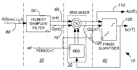
Referring to Figure 6, a demodulator 10
according to an embodiment of the invention is
illustrated. The three stages of the demodulator are
as follows: a conversion stage 20, a mixer stage 30,
and a phase quantizer stage 40. In the following
description the demodulator 10 will be referred to as
a CVo~PLL meaning a complex valued delta sigma phase
locked loop demodulator. To try to make the
description more clear some assumptions are made so
that CVo~PLL can be described by example. One of
these assumptions is that the IF frequency which the
CVo~PLL is required to demodulate is 45 MHz . Also
low side LO frequencies are assumed everywhere. In
cases where a resulting second (or third etc.) IF
involves a complex signal, it is assumed that the
positive rotating exponential is desired rather than
the negative rotating exponential. Clearly the
functionality and implementation techniques described
here apply equally well to other IF or LO frequencies
and equally well to negatively rotating exponentials
as well as positively rotating exponentials for
complex signals. ,
The CVo~PLL obtains and processes amplitude
information by using in phase and quadrature samples
3.5 of the input signal. These provide a complex
CA 02422794 2003-03-18
WO 02/25803 PCT/CA01/01338
representation of the input signal as a phasor with
Cartesian components. In a preferred embodiment,
some sampled signal, x1 has a real and an imaginary
part, once it is sampled. Linear filtering can then
be performed on these components. Other operations
can be performed more "easily'.' when the signal is
treated as a magnitude, M1, and a phase, 8, Since it
is ultimately the rate of change of phase
(frequency) , .fl, which we wish to extract from the
signal, the CVd~PLL can be thought of as a o~ phase
locked loop like the previous o~ PLLs with the
exception that now the amplitude information is
available as an output rather than thrown away at the
very front end.
The CVo~PLL can be viewed as an extension
of existing o~ techniques by adding PLL concepts, or
as an extension of existing PLL techniques by using
noise shaping and discrete time signal processing.
The approach used here to explain the demodulator
comes at it from the PLL point of view.
As can be seen from Figure 6, the CVo~PLL
consists of:
- a Hilbert Sampler/Filter 50 which
provides a complex representation of the
continuous time input signal having an
inphase 60 and quadrature 70 signals to
represent the phasor or complex envelope of
the input signal 80.
- a DDS-mixer 90 which performs a discrete
phase shift (or rotation in the complex
plane) of the input inphase 60 and
quadrature signals 70 in response to a
bitstream output signal 100 (nT) to produce
two signals, A(nT) and Qq(nT), (the
26
CA 02422794 2003-03-18
WO 02/25803 PCT/CA01/01338
amplitude output 110 (A(nt)) and an
intermediate complex signal 120 (Qq(nT))
- a phase quantiser which quantises the
phase angle of the complex signal A(nT) + j
Qq(nT) to produce the bitstream signal
b(nT) 100.
The bitstream output 100 is fed back to the
DDS-Mixer which corrects the phase of the complex
signal A(nt) + j Qq(nT). The phase angle of A(nT) +
j Qq(nT) is decreased if the phase signal angle is
greater than 0 and increases the phase angle if the
phase angle is less than 0.
One key feature which distinguishes the
CVo~PLL from the CVPLL is the use of discrete time
analog processing for the quantisation of the phase
error and the phase shift introduced by the DDS-
mixer. This allows the use of a DDS-mixer combination
instead of a continuous time VCO and a mixer
combination. The presence of a quantiser also
distinguishes the CVo~PLL from the CVPLL (Figure 5).
The feature which distinguishes the CVo~PLL
from the o~PLL is the use of complex signals to
retain both the magnitude and the phase of the input
signal or equivalently both the inp~hase and
quadrature components of the input signal.
Within the context of the CVo~PLL, there is
a wide variation of possible architectures and
implementations. These variations, involve
variations in the Hilbert Sampler/Filter, the DDS-
mixer and the optional use of filtering and/or extra
downconversion stages between the DDS-mixer and the
Phase-Quantiser.
Variations in the Conversion Staae
The primary function of the Hilbert
Sampler/Filter 50 is to provide an in-phase and
quadrature representation of the input signal to pass
27
CA 02422794 2003-03-18
WO 02/25803 PCT/CA01/01338
on to the DDS-Mixer. An optional.secondary function
is to filter undesired signals from the input signal
or to filter undesired signals added within the
Hilbert Sampler/Filter itself.
The Hilbert Sampler/Filter function can be
realized with either:
IQ down-conversion alone,
- complex filtering alone,
- sampling alone, or
- sampling in conjunction with discrete
time filtering.
Sampling in the Hilbert Sampler/Filter is
not necessary if the subsequent stages, the DDS-Mixer
and the phase quantiser, can function with continuous
time signals.
In the case of IQ downconversion alone,
some low pass filtering would be required to remove
the negative frequency components at -fIF-.f~. The
quality of the in-phase and quadrature match will
limit the removal of frequency components at -fze-.f~~ .
This in turn will limit the accuracy of the phase
angle of the complex signal intended to describe the
IF phasor or complex envelope.
The IQ downconversion could be obtained in
25, very conventional ways. For example, an ECL divide by
4 circuit could be used to divide a 178 MHz reference
down to an (f~ = 44..5 MHz) in-phase and quadrature L0.
Then two Gilbert-cell mixers could downconvert the IF
signal. The low pass filtering could then consist of
just two RC low pass filters to attenuate the
frequency components at -fIF-.fc. If these parameters do
not provide enough attenuation, then the second IF
frequency -fIF-.fc could be reduced to a lower
frequency, or the order of the filter increased.
Alternatively, if downconversion is not
desired to reduce the operating frequencies of the
28
CA 02422794 2003-03-18
WO 02/25803 PCT/CA01/01338
subsequent components in the CVo~PLL, then the in-
phase and quadrature signals may be obtained by
directly filtering the IF signal with a complex
filter. By setting the imaginary input to the complex
filter to ground and the real input of the filter to
the IF signal, we can tell the filter that its input
is J +jQ where the imaginary part, Q, is set to zero
and the real part, I is the (real) IF signal. The
output of the complex filter then provides a complex
signal at 45 MHz. The accuracy of the two resulting
signals (as a representation of the complex envelope
of the input signal) is limited by the matching of
the components in the filter.
Another alternative would be to sample the
input signal. For any sampling frequency chosen, it
is necessary to filter the 45 MHz IF signal to
sufficiently anti-alias it before entering the
CVo~PLL or before the sampling operation occurs
within the Hilbert Sampler/Filter.
Other techniques are available to obtain
in-phase and quadrature samples. For example, two
track,and hold amplifiers could be used. By switching
the two amplifiers into hold mode at different times,
separated in time by a delay equal to 1/4 of an IF
period, or (n+ 1/4) of an IF period where n is an
integer. The track and hold amplifiers must have
sufficient bandwidth for the 45 MHz IF signal even if
they are sampled at a rate substantially less than 45
MHz. Another example would be to use one track and
hold amplifier to produce both the I and Q outputs in
a multiplexed stream. Depending on the details of the
subsequent components of the CVo~PLL, these signals
may have to be demultiplexed and/or retimed to be
compatible with the other components.
Optionally, discrete time filtering may be
used to reduce negative frequency exponentials in the
29
CA 02422794 2003-03-18
WO 02/25803 PCT/CA01/01338
complex representation made by I' +j Q'. Just as a
continuous time complex filter can derive in-phase
and quadrature signals from a real input signal, a
discrete time complex filter can be used to obtain a
complex representation of a single sampled signal by
suppressing the negatively rotating exponentials. The
filtering may also be used to reduce the effects of
interfering signals and noise.
However, it is preferred that the
conversion stage beta Hilbert Sampler/Filter. Figure
7 illustrates such a Sampler/Filter. As can be seen,
the Sampler/Filter has:
- a circuit element 200 with:
- a transconductance Gm, resistance or
other conversion means to obtain a current
proportional to the input IF signal,
- a series of sampling phases, P1 ... Pn,
only one of which is high during a
predetermined time interval, which provide
complex co-efficients of an FIR filter by
switching the destination of the current
source to one of,
- a predetermined number of capacitors, to
integrate the current over each of the
predetermined time intervals when the
current is sent to that capacitor,
- a means to transfer the charge, or the
information associated with the charge, on
some or all of the capacitors to the next
stage after the~Hilbert Sampler/Filter or
to subsequent filter stages within the
Hilbert Sampler/Filter.
The circuit can be generalized as a number
of sampler cells, each sampler cell 125 as shown in
Figure 8. As can be seen, each sampler cell has a
buffer 130, a data transmission switch 140, a sampler
3O
CA 02422794 2003-03-18
WO 02/25803 PCT/CA01/01338
switch 150, a capacitor 160, a grounding switch 170,
a first connection point 180. The circuit element
200 with transconductance Gm is coupled to each
sampler cell. In Figure 7 and 8, cpl, represents the
time the grounding switch 170 is closed.
represents the time the data transmission switch 140
is closed.
The key feature of this type of sampler is
that the signal is integrated over an entire interval
rather than sampled at the end of an interval. By
arranging the timing of Ti and Ta (Ti represents the
time interval that each of the sampler switches is
closed while Ta is the total time interval between
the closing of the first sampler switch P1 to the
opening of the last sampler switch Pn), each of the
phases P1 to Pn can function as complex coefficients
of an FIR filter, prior to an ideal sampling. The
previously discussed complex filters provided only
delay functions, e'SnT, to form the basis of a filter
prior to sampling. Then, by selecting how the samples
were used, complex coefficients could be introduced
to reduce negative frequency exponentials. The new
complex filters provided by this sampler provides an
improved filter element (e S(n+1)z _ a snT~ ls. The phases
P1 to Pn can then be used to provide complex
coefficients of an FIR filter to reduce negative
frequency exponentials prior to sampling.
A simple version of this sampler.can be
built as shown in Figure 7. In this simple case,
there are only 4 phases and 4 capacitors. Each
capacitor voltage integrated during P1, P2, P3 or P4
is buffered with a unity gain buffer and applied to
subsequent filtering stages or the DDS mixer during
~2. The switches clocked on ~1 and cp2 and the unity
gain buffer are one means of sampling the charge
31
CA 02422794 2003-03-18
WO 02/25803 PCT/CA01/01338
stored in the capacitors and transferring the
information to later stages. Other means of
transferring this charge to the DDS mixer are
discussed later. As part of this scheme, the
capacitor voltages are reset to ground during ~1.
In this, and all examples to follow, it is
assumed that only 1 sampler switch is closed during
any one time interval. At the detailed circuit
design level, switches have finite rise and fall
times on the switch control signals. It can be
difficult to assure that P2 rises at precisely the
same time P1 falls. Further, it may be desirable to
have some overlap so that, in this example, P2 rises
before Pl falls. Thus, when we say only one sampler
switch is closed during any one time interval, this
is meant as a first level of understanding only. In
practice, the phrase is intended to include
embodiments where there is substantial overlap
between each sampling interval and the next as well
as when there is a gap between time intervals.
A typical timing diagram might be as
follows in Figure 9. Here, Ta is the aperture time
of the sampler, or the time interval over which the
sample is made. In this example Ta is included in
neither the time when ~1 is active nor the time when
~2 is active. That is, it has its own time slot. In
this example, the time slot for Ta occurs between ~1
and ~2. Clearly, manyother arrangements are
possible, or may be required to adapt to other
30' components used with the sampler.
The Hilbert Sampler/Filter of Figure 7 may
also optionally include repeated sequences of complex
tap coefficients. For example, the switch controlling
the current to Cl could close two or more times
within the aperture time Ta. An example where each
switch is closed 3 times is illustrated in the timing
32
CA 02422794 2003-03-18
WO 02/25803 PCT/CA01/01338
diagram of Figure 10. Keeping Ti constant, Ta
increases and. the filter becomes more selective.
Tn the previous example there were 4 phases
- one for each capacitor. For one capacitor to
integrate over 3 time intervals, Ti, each phase went
high 3 times. As an alternative, the same function
can be provided with n phases, P1 to Pn each of which
is high only once during Ta. For example, to achieve
the same filter prior to sampling as the previous
example, we could pick n = 12. Then the timing,
diagram would be as shown in Figure 11.
The timing diagram of Figure 11 can be
obtained simply by "unrolling" the timing diagram of
Figure 10. Thus, P1, P5 and P9 in Figure 11
correspond to the three times the first phase (P1) of
Figure 10 went high.
Now three switches controlled by P1, P5,
and P9 control when the current is switched to Cl.
Clearly the other capacitors receive current in a
similar way under the control of the other phases.
This arrangement is particularly convenient when Ta
is equal to the period, Tr; of some reference clock
already available on an integrated circuit for other
purposes. Then the phases P1 to Pn can be obtained
from a Delay Locked Loop locked to this reference.
The two techniques may also be combined
such that the phases P1 to Pn repeat, for example as
shown in the Figure 11B where Ta = 2Tr. Clearly, the
approach could be extended to Ta = pTr where p could
be more than 2. Also, not all of the available time
intervals need to be used. To be even more general,
it should be noted that Tr could result from dividing
down some higher frequency reference.
Another layer of generality may be added by
including some additional logic such that P1 assigns
the current to a particular capacitor during one
33
CA 02422794 2003-03-18
WO 02/25803 PCT/CA01/01338
cycle of the reference but to some other capacitor
during another cycle of the reference. By also
including logic such that the current may be switched
directly to ground without going through a capacitor,
the phases P1 to Pn can also generate coefficient of
value 0 in addition to 1, j, -1 and -j.
So far we have assumed that Ta < Ts where
Ts =.l/fs is the period of sampling the charge stored
onto the capacitors. This restriction may be avoided
by using multiple instances of the sampler. By having
two or more samplers that are well matched, the
sampler can be pipelined such that one sample becomes
ready every Ts seconds while the others are in the
process of completing their sample. Mismatch in the
capacitors or transconductances result in different
gains on each of the interleaved samplers. With the
voltage-buffer charge sampling means shown in these
examples capacitor mismatch causes the same
difficulty.
While the above circuit only had four
sampler cells, multiple cellular Sampler/filter
circuits can easily be constructed. The timing
diagrams of Figures 11A & 11B can also be applied to
a sampler/filter circuit such as that illustrated in
Figure 7 but with twelve sampler cells instead of
four. This has the advantage of reducing the
quantization step size S.
Figure 12 illustrates one way to build the
transconductance element (200 in Figure 8)and
switches (150 in Figure 8) in an integrated circuit.
Figure 12 shows a schematic of one way to build the
charge sampler in an integrated circuit. In this
example, the circuit element 200 is a differential
pair 210. The input voltage is applied to a
differential pair of MOS transistors whose g~" is
34
CA 02422794 2003-03-18
WO 02/25803 PCT/CA01/01338
controlled by the tail current of the differential
pair. This provides an adjustable transconductance gm
which can be used for AGC in the receiver. It also
provides a differential current source. Most of the
~ common mode current of this differential pair is then
absorbed by a pair of common mode feedback
transistors while some of the common mode current and
all of the difference mode current is cascoded into
either the positive supply or into two of the four
capacitors.
The switches of the sampler are provided by
NMOS transistors with their gate voltage controlled
by the phases P1 to Pn. By setting the high level for
P1 to Pn at 2.5 V rather than the 5V supply, a
1S virtual ground is provided to reduce the effects of
non-linear output impedance of the current source. To
assure that this virtual ground is maintained at all
times, a new phase PO is provided which is high
whenever the other phases are not.
This way, the cascode transistors for the
folded cascode are also used as switches to determine
which load capacitor, if any, gets the difference
mode current and residual common mode current. Each
load capacitor then integrates the current over the
duration of the time that the switches connecting it
to the current source are closed. C1 is assigned to
represent the inphase channel sample and C3 to
represent its compliment (or phase shifted by 180
degrees). Similarly C2 is assigned to represent the
quadrature channel and C4 to represent its
compliment. Now by arranging the P1 to Pn phases to
switch the Current into one of the 4 capacitors, the
switches can be used to form complex tap coefficients
of an FIR filter. If capacitor C1 accumulates a
3S voltage interpreted as the inphase component, any
3S
CA 02422794 2003-03-18
WO 02/25803 PCT/CA01/01338
time interval above current is switched to provides a
+1 co-efficient for a top of an FIR filter.
Similarly, if C2 accumulates the complimentary
voltage to Cl, time intervals assigned to this
S capacitor provide -l top co-coefficient. C3 and C4
can be further used to provide +j or -j coefficient.
Coefficients of value 0 can be provided by PO which
shunts the current to the positive supply.
This example does not illustrate the buffer
(130 in Figure 8) and transmission switch (140 in
Figure 8) of each cell. The nodes V1 V2 V3 and V4
correspond to the first connection point (180 in
Figure 8) for each of the four cells.
This example illustrates a four phase
sampler, where the complex tap coefficients of the
filter are restricted~to the set {0, +1, -1, +j, -j}.
That is, it can provide tap coefficients of magnitude
0 or 1 where the coefficients of magnitude 1 can have
four angles, separated by 90 degrees in the complex
plane. The example can be readily extended to provide
an 8 phase filter with 8 cells. Then, the 8 cells
provide tap coefficients of magnitude 0 or 1 where
the coefficients of magnitude 1'can have 8 angles,
separated by 45 degrees in the complex plane.
Generally, tap coefficients of separation 360/N
degrees in the complex plane can be provided by N
sampling cells. FIR sampling filters can then be
formed by selecting a particular sequence of tap
coefficients through the sequence of closing switches
in the switch matrix.
In this case, the grounding switches (170
of Figure 8) are provided by the PMOS transistor M7
(only one of 4 is shown). Each of these shorts a
capacitor to ground during ~1. Ground in this example
is the positive supply but in general it can be any
predetermined voltage.
3G
CA 02422794 2003-03-18
WO 02/25803 PCT/CA01/01338
A number of issues must be taken into
account when using this approach. An adequately
accurate phase shift of 180 degrees between Vip and
Vim is required. Specifically, common mode voltage
fluctuations at 45 MHZ should be avoided. The exact
relationship between Iagc and the amount of gain
control obtained is process dependent.
The current source, Iagc, may be used in a
feedback loop developed later in the discriminator
which detects the amplitude of the desired signal
after filtering. Alternatively it may be a D/A
converter. The amplitude of the desired signal should
be adjusted to allow overhead for the undesired
alternate channel within'the linear range of the
sampler. This AGC feedback signal could also provide
the RSSI signal required in other parts of the
receiver.
The voltage source, Vcmfb, is intended to
be used as. common mode feedback to pin the common
mode of the sampled output to a suitable voltage
below the positive supply. There are at least two
options for developing the CMFB voltage. One option
is to force the opamps in the complex resonator to
transfer the difference mode charge onto the
integrating capacitor without affecting the common
mode charge. Another option is to add a second set of
sampling capacitors and arrange the switches such
that only common mode charge is integrated. In either
case, we can be left with a common mode voltage, Vcmr
on a capacitor which can be sampled and used to
develop
However, the structure of Figure 8 is not
the only way to construct a sampler cell for a
Hilbert Sampler/Filter. The sampler cell may also be
completed by transferring the charge to a virtual
37
CA 02422794 2003-03-18
WO 02/25803 PCT/CA01/01338
ground 240. This is illustrated by example in Figure
13a where the virtual ground is formed by an opamp
220 and a feedback impedance 152 placed after the
Hilbert Sampler/Filter. Since the transconductance
element drives a virtual ground in this embodiment, of
the Hilbert Sampler/Filter the requirements for
output impedance and compliance voltage of the
circuit element are reduced. As a result, this is the
preferred embodiment of the Hilbert sampler/filter.
It Comprises: a circuit element having a
transconductance and a plurality of sampler cells,
each sampler cell comprising a sampler switch coupled
between the circuit element and a virtual ground;
wherein for the plurality of sampler cells, only one
sampler switch is closed during any one time
interval.
There are many other virtual grounds
available~in the literature other than the inverting
input of an amplifier. The term virtual ground is
intended here to encompass any technique that holds
the voltage of the virtual ground close to a
predetermined voltage through feedback. This includes
techniques such as a cascode transistor where the
feedback may be internal to the transistor or
external to the transistor through gain boosting.
Just as in the embodiment of Figure 12, the
number of phases in the sampler/filter is determined
by the number of sampler cells. Similarly, the number
of available tap coefficients and their separation
(in degrees) in the complex plane is determined by
the number of virtual grounds. Also as with the
embodiment of Figure 12, the sequence of the tap
coefficients is determined by the sequence of switch
closings. .
Similarly to the embodiment of Figures 8
and 12, this embodiment of the Hilbert sampler/filter
3s
CA 02422794 2003-03-18
WO 02/25803 PCT/CA01/01338
may further comprise a sampler cell coupled between
the circuit element and a ground to provide a tap
coefficient of value 0.
The Hilbert sampler/filter may also further
comprise additional filtering provided by the
feedback. For example, if the feedback impedance 152
in Figure 13a were a resistor in parallel with a
capacitor, a real, single-pole low pass filter would
be provided in addition to the FIR filter provided by
the sampler cells and the circuit element.
Figure 13b illustrates a sampler cell where
this feedback impedance is a switched capacitor
resistor.
As can be seen, the sampler cell of Figure
13 has a sampling switch Pi, a sampling capacitor Ci,
a filtering sampling switch Csi, primary switches
clocked by ~1, and secondary switches clocked by c~2.
A first sampler node 230, second sampler node 240m
third sampler node 250, and a fourth sampler node 260
are illustrated in the figure.
From the figure, a primary switch clocked
by ~1 is between ground and the fourth sampler node
260. Another, primary switch clocked by cpl, is
between the third sampler, node 250 and ground. The
filtering capacitor is coupled between the third
(250) and fourth (260) sampler nodes. a secondary
switch ~2 is between the second (240) and third (250)
sampler nodes while the other secondary switch ~~ is
between the first (230) and fourth (260) sampler
nodes. The operational amplifier 220 is coupled
between the second (240) and first (230) sampler
nodes. The negative input of the opamp is coupled to
the second (240) sampler node while the positive
input is coupled to a reference voltage VREF. The
sampling switch Pi is between the second (240)
sampling node and the cell input. The sampling
39
CA 02422794 2003-03-18
WO 02/25803 PCT/CA01/01338
capacitor Ci is coupled between ground and the second
(240) sampler node.
The feedback impedance may also be made
complex by the circuit shown in figure 14. The pair
of sampler cells in Figure 14 have a phase separation
of 90 degrees. That is one represents an inphase
component and the other a phase shifted version of
the complex signal. Traditionally the phase shift
between the two is 90 degrees so that the other
component is a quadrature component but with more
than two phases other phase shifts are possible.
Clearly, the single pole filter shown in Figure 14
could be extended to a biquad or cascode of biquads
using well known techniques commonly applied to
discrete time filtering.
Figure 14 illustrates a.pair of sampler
cells. The pair of cells have a pair of operational
amplifiers 270, 280, a pair of filtering capacitors
Ci (290, 300), primary sampling capacitors 310, 320
(Cr) , secondary sampling capacitors (Cp) , 330, 340, a
first sampling switch 350 for the first cell and a
second sampling switch 360 for the second cell. Also
shown in the diagram are eight primary sampling
switches 370, 375, 380, 385, 390, 395, 400, 405 and
eight secondary sampling switches 410, 415, 420, 425,
430, 435, 440, 445. Also included in the pair of
sampler cells is a negator 450. For ease of
description, a number of nodes are also identified:
- first intermediate node 460
- second intermediate node 470
- third intermediate node 480
- fourth intermediate node 490
- fifth intermediate node 500
- sixth intermediate node 510
- a seventh intermediate node 461
- an eighth intermediate node 471
CA 02422794 2003-03-18
WO 02/25803 PCT/CA01/01338
- a ninth intermediate node 462
- a tenth intermediate node 472
along with a first output node 520 (the output of
opamp 270, and a second output node 530 (the output
of opamp 280).
The first sampling switch 350 is between
the input to the cell pair and the first intermediate
node. The second sampling switch 360 is between the
input to the cell pair and the second intermediate
node. The first intermediate node is coupled to the
negative input of the opamp 270. The second
intermediate node is coupled to the negative input of
the opamp 280. Both positive inputs of the two
opamps 270,280 are coupled to ground. Each of the
filtering capacitors 290, 300 are coupled across the
negative input of an opamp and the output of the same
opamp.
Coupled between the seventh intermediate
node 460 and the third intermediate node 480 is a
primary sampling capacitor 310. Similarly, the
second primary sampling capacitor 320 coupled between
the eighth intermediate node 471 and the fourth
intermediate nodes 490. The secondary sampling
capacitors 340 is coupled between the ninth
intermediate node 462 and the fifth intermediate node
500. The other secondary sampling capacitor 330 is
coupled between the tenth intermediate node 472 and
the sixth intermediate node 570.
Concerning the primary and secondary
sampling switches, the eight primary sampling
switches are each coupled between ground and one of
the following nodes: the third, fourth, fifth, sixth,
seventh, first, second and eighth intermediate nodes.
Of the eight secondary sampling switches, one (410)
is coupled between the second output node' 530 and the
fourth intermediate node. 'Similarly, another (440)
41
CA 02422794 2003-03-18
WO 02/25803 PCT/CA01/01338
is coupled between the 3rd intermediate node and the
first output node 520. Another (switch 430) is
coupled between the fifth intermediate node 500 and
the second output node 530. Another secondary
sampling switch 420 is coupled between the sixth
intermediate node 510 and the negator 450. The
negator 450, in turn is coupled between the secondary
sampler switch 420 and the second output port 520.
The fifth secondary sampler switch 445 is coupled
between the seuenth and the first intermediate node.
Another secondary sampler switch (435) is between a
primary sampler switch (385) and the ninth
intermediate node. A further secondarv sampler
switch (425) is between another primary sampler node
(395) and the tenth intermediate node. The final
secondary sampler switch 415 is between the second
intermediate node and the eighth intermediate node..
In the circuit of Figure 14, the sampling
capacitors are CR and Cp. The phases P1 to Pn may be
contained within one of the switched capacitor
phases. Alternatively, Ta may occur during one of
the switched capacitor phases. The circuit of Figure
14 can be clocked with the timing indicated in Figure
15 to show an example where Ta occurs during cpl. With
this arrangement of the timing, the current source
can drive a virtual ground.
The circuit of Figure l4 is shown single
ended for clarity; it may be better to use
differential circuitry with common mode feed=back.
Then, P3 would provide the compliment of P1, P4 would
provide the compliment of P2 in a phase example. The
technique can be readily extended to more phases.
Another means of transferring charge from
the sampler is to use passiue switched capacitor
techniques. This can also be used to provide
additional filtering The absence of opamps may make
42
CA 02422794 2003-03-18
WO 02/25803 PCT/CA01/01338
the passive approach more linear and more suitable to
low voltage applications. In this case, the means of
transferring charge out of the sampling capacitors is
simply a series of switches connecting the capacitors
to the next stage of the Hilbert Sampler/Filter or
the DDS-Mixer.
An example is shown in Figure 16. In this
case charge balance equations on any one.of the
output voltages give
T~(z) = 1 1 _1 Q; (z) Whe~~e CT = Ca + Cbafzd Y = Cb l C,..
CT 1 + yZ
Thus, each pair of Ca and Cb capacitors
forms a single pole real filter. Now if each of these
filters match the others, we have the same filter
applied to each of the I and Q channels as well as
there compliments. Under these conditions we have the
equivalent of a real filter applied to a complex
signal.
Complex filtering may be provided. in many
ways to improve the rejection of negative frequency
exponentials.
It should be noted that the circuit of
Figure 16 is similar to that of Figure 7. However,
each sampler cell of Figure 16 has an extra filtering
capacitor (CbX) after the sampler switch cp2.
The concepts embodied in the sampler/filter
illustrated so far may be extended to apply to a new
type of discrete~time complex filter which is made up
of:
- an information sampling means which can
sample three or more phase-shifted versions
of the input signal, shifted uniformly
through 360 degrees in the complex plane,
43
CA 02422794 2003-03-18
WO 02/25803 PCT/CA01/01338
producing three or more corresponding
phases;
- one or more groups of information storage
means where each individual information
storage means in a group stores information
for each phase of the sampling means and
provides a value to represent this
information;
- optionally, a means of transferring
information from one group to the next and
finally to an output group if there is more
than one group.
one or more groups of information sharing
means for sharing information between, the
~ previous time value of each phase and a
rotating phase-shifted version of the
previous-time value of each phase; and
- a means to pass some or all values of the
output group to other circuits.
The filter has. been described here in very
abstract terms because it could provide a discrete-
time digital filter as well as a discrete-time
analogue filter, The discrete-time digital filter
(and the discrete-time DDS-Mixer to follow) could be
used after A/D conversion in a digital filter built
of adders and multiplexers or with fixed point DSP in
a microprocessor. Either of these options would
require some intelligent noise shaping approach to
round off error.
One example of an analogue four-phase 1-
group filter is shown in Figure 27. In this case the
information sampled is charge sampled by integrating
current over the time intervals P1 to P4. The
information storage means are each equally weighted
capacitors of the Cb group of capacitors. The
44
CA 02422794 2003-03-18
WO 02/25803 PCT/CA01/01338
information sharing means are each equally weighted
capacitors of the Ca group of capacitors, the switch
control signals K1 to K4 and the switches operating
under the control of KI to K4. The phases Kl to K4
are arranged to be active during the time when ~l is
active and to have the same duration as ~1 Each of
these phases Kl to K4 have a period of 4 times the
period of cp1 and are phased such that only one of
them is active at any one time so that each eb
capacitor is connected to one Ca capacitor during ~1,
as illustrated in the timing of diagram of Figure 18.
As can be seen from Figure 17, the
sampler/filter circuit can be viewed as a collection
of primary sampler cells, each of which can be
connected to a collection of secondary sampler cells.
A circuit element 540 with a transconductance Gm is
coupled at a common node 550 to a grounding switch
560 which is, in turn, coupled to ground. The common
node 550 couples each of the primary sampler cells to~
the circuit element 540.
Figure 19 illustrates a single primary
sampler cell coupled to four secondary sampler cells.
As can be seen from Figure 19, a first capacitor 570
(Cb1) is coupled between ground and a first
connection node 580. Between the node 550' and a
primary sampler cell output V1, is a buffer 590.
Between the node 570 and a second connection node 600
is an activation switch 610 (~1).
Between the node 600 and the circuit
element 540 is a sampling switch 620 (P1). Coupled
to the node 600 are the secondary sampling cells.
Each of these secondary sampling cells are coupled to
the node 600 by an array of coupling switches. Each
secondary cell~is composed of a second capacitor 6301,
630, 6303, 6309, coupled between ground and a
CA 02422794 2003-03-18
WO 02/25803 PCT/CA01/01338
corresponding coupling switch, 6401, 640, 6403, 640Q.
By closing one of these coupling switches, any one of
the second capacitors can be coupled to the primary
sampler cell. Between Figures 17 and 19, it should
be clear that any one of the secondary sampler cells
can be coupled to any one of the primary sampler
cells.
The key feature illustrated in this passive
filter is that one set of capacitors rotates relative
to another set of capacitors. For example, in Figure
17 capacitor Cbl, is connected to capacitor Cal then to
Ca2i Cas. Ca9. and back to Cal. This process repeats
indefinitely. The point of this arrangement is that
on each connection, cpl, the Cbz capacitor is connected
to a Ca capacitor which was previously connected to
Cb~. Thus on every connection phase, a charge sharing
operation occurs between the previous voltage V1 and
the previous voltage V2 through the~capacitors Cbl and
one of the Ca capacitors .
Any of the sampler/filter circuits.
discussed above, and their equipments or extensions,
can be used for the conversion stage of the CVo~PLL
demodulator.
Variations on the Mixer Staae
Since the CVo~PLL demodulator needs to mix
and phase lock to a specific frequency, PLL concepts
call for a signal to mix the incoming signal with.
Experience and experiments dictate that a direct
digital synthesizer (DDS) provides the best results
for the CVo~PLL. Thus, in the following discussion,
the mixer stage will be referred to as a DDS-Mixer.
It should be noted that, as the conversion
stage produces 2 signals, the inphase and the
quadrature representations of the demodulator input,
the DDS-Mixer receives both these signals.
46
CA 02422794 2003-03-18
WO 02/25803 PCT/CA01/01338
The primary function of the DDS-mixer is to
provide discrete phase shifts of. the output of the
Hilbert Sampler/Filter. These phase shifts respond to
the output of the Phase Quantiser to provide a
negative feedback adjusting the phase~of the DDS-
mixer output toward some predetermined value. An
accumulation means, typically a digital phase
accumulator, (DPA) responsive to the output bit
stream, b(nT), integrates the bit stream to provide a~
state, 0, which indicates the required degree of
phase shift for the input signal, Xos= I+jQ. The mixer
part of the DDS-mixer provides an output Xrl = A +j~g
such that Xrl = Xos e-'e. A wide variety of circuits to
accomplish this are presented in the literature and
are known to those versed in the art.
The DDS-Mixer may also provide a frequency
offset control. When this is provided, additional
frequency offsets may be removed from the Hilbert
Sampler/Filter output. Figure 20 shows an example
where a digital adder 650 is used to add the
frequency offset control to the bit stream, b(nT)
660. In cases where the digital phase accumulator
(DPA) provides a separate carry input for the LSB and
the bit-stream, b(nT), is a single bit bit-stream,
the frequency offset control can consist of applying
a frequency offset control word to the main DPA input
and the bit-stream to the carry input, of the DPA.
The DDS-Mixer may also optionally provide
additional filtering to provide a filtered output,
Xr2(nT) - A(nT) +j Qq(nT). This filtering provides
reduction of undesired signals present in the
original IF input, or reduction of undesired signals
introduced by the DDS-Mixer or Hilbert
Sampler/Filter. Generally, this filtering could be
either real or complex.
47
CA 02422794 2003-03-18
WO 02/25803 PCT/CA01/01338
A simple implementation of the DDS/mixer
combination is presented in Figure 21. In a
conventional DDS the input frequency is accumulated
in a phase accumulation register 670, to provide a
value, 8, representing the DDS phase. The output
phase is then passed to a sine 680A and cosine 680B
lookup ROM to provide the complex output after a pair
of D/A converters 690. In the simple implementation,
each of the sampled inputs would then have to be
multiplied by the real and imaginary outputs from the
DDS: The four quadrant multiplication mean 700 could
then take the form of a Gilbert cell multiplier or
some other equivalent. Clearly this implementation
would be complicated. The lookup ROMS and mixers can
be replaced with switched capacitor circuits.
When three or more phases of the Sampled
sign are available, a DDS mixer with a phase
resolution corresponding to the. number of available
phases can be produced through the mixing properties
of°the switch matrices discussed for filtering.
As with the DDS-Mixers previously
described, an accumulator responsive to the output'
bit stream, b(nT), integrates the bit stream to
provide a state, 8, which. indicates the required
degree of phase shift for the input signal, Xos =
I+jQ. Two approaches to making the switches have
been identified. One approach is to have a digital
decode and dedicated switches. That is for example, a
16 x 16 switch, can be made up of 256 individual
switches of which 16 at a time can be turned on to
connect 16 phases on one side of the switch to 16
phases on the other side of the switch with the
desired degree of rotation controlled by digital
logic. Alternatively, the switches may be connected
in series to perform the decoding directly~from the °
4~
CA 02422794 2003-03-18
WO 02/25803 PCT/CA01/01338
state of a digital phase accumulator. Combinations
of the two approaches are, of course, also possible.
One method of implementing the DDS-Mixer
with additional filtering uses switched capacitor
techniques as described. To simplify the DDS, its
resolution is reduced to 4 bits or 16 possible
states. As a result, 8 can take on only 16 possible
values. In the example presented here, 8 is
accumulated in a digital phase register (as in a
conventional DDS) however the value in the phase
register is used to directly select one of 16
possible phase shifts of the sampled signal. This
avoids the need to implement the ROMs D/As and
mixers.
Mathematically, we wish to generate
Xr1 - A~ + J Q~g
from the input signal
Xos = I + jQ which is provided by the
Hilbert Sampler/Filter
That is we want
-ae
~r~ - Xose
and pass this to the opamp rather than the original
sampled signal. In terms of real and imaginary parts,
the above expression becomes
Re (Xrl) - Re (Xos) cosh - Im(Xoa) sin~
Im (Xrl) - Re (Xos) sin6 + Im (Xas) cosh
With the quadrature sampler, phase
shifts of n/2 or multiples of n/2 are easily
performed by swapping and/or inverting the in-phase
and quadrature samples. In this way the two MSBs of
the 4 bit DDS/mixer can be implemented with only
switches. The remaining 2 bits require phase shifts
of multiples of n/8. These can be arranged through
capacitor ratios shifting only a portion of the
charge between the sampler's in-phase and quadrature
49
CA 02422794 2003-03-18
WO 02/25803 PCT/CA01/01338
channels. The above equation suggests that maybe the
sampled charge (on each channel) could be divided
into two portions; for example on the in-phase
channel, a portion of the charge proportional to cose
would remain on the in-phase channel while a portion
of the charge proportional to sin6 would be passed to
the quadrature channel. While this suggestion is
true, it turns out that it cannot be implemented~with
two capacitors because, in general,
sin' (8) + cost (0) - 1 and sin(~) ~+~ cos (8) ~ 1.
This causes difficulties because the total
charge sampled onto only two capacitors cannot be
divided up into two portions proportional to cosh and
sin6 for all values of 6. As a result, a third
capacitor, C13 and C~3 is needed on each of the in-
phase and quadrature channels as shown in Figure 22.
In Figure 22, the practice of showing the
circuit single ended is used again for clarity and
simplification. Here the transconductance is shown as
a simple current source switched onto the load
capacitors for a period cpis. In this scenario, we
sample a charge, Q, onto C11, Ci2, and Ci~. Since the
same voltage occurs across the three capacitors, the
charge in the capacitors is
CIf ~ ~ C21 ~ ~ C31
t ( 1
CT CT CT
and similarly for the quadrature channel,
C19 Q Cz4 n C39
9 9 CT + R CT + g CT
CA 02422794 2003-03-18
WO 02/25803 PCT/CA01/01338
Both of these sampled charges together can
be expressed in complex notation as, QS = Qi + jQq.
The switches active during ~2 can then be arranged
such that the charge passed on to the opamp during ~2
C11 - ~ C29 + ~ ~ ~19 - _C2i
os = t g g
CT CT CT Ct
Now by selecting
C'' =acosB
CT
C~ 9
= aSllle
CT
=aS1118
CT
CZ' = a COS B
CT
we have
QoS = a~(Qt cos 9 -~Qy sin 9) + j (Qv sin B - Qt cos 9)]
which gives
C3 =1- a (cos B + sin 8)
CT
These equations can be solved for each
value of 8. Then the phase, ~, stored in the digital
51
CA 02422794 2003-03-18
WO 02/25803 PCT/CA01/01338
accumulator can be digitally decoded to switch the
appropriate set of sampling capacitors into the
sampler. Thanks to symmetry in the quadrants, there
will only be four sets of capacitors to switch for
this 16 phase example.
Since C3contains a charge that will be
thrown away, it represents a signal loss and we would
like to keep it as small as possible in every case
for 6 The smallest value for C3 occurs when 8 is a
multiple of n/2. When O= n/4,
cos 8 = sin B = ~ 11~I21CI7 7371217"32 g'7l~eS C1 =
Figure 2~ shows a simplified version of the
sampler-DDS/Mixer-Filter combination. It is
simplified in several ways. As with the previous
filter schematic, it is shown as a single ended
circuit where it is intended to be differential. The
sampler operation has been simplified to a switched
current source where HIS represents the cascode
switches discussed in the previous section. The
digital phase accumulator of the DDS is not shown,
and the decode logic to generate ~IDDS or ~=.DDS is not
shown. Further, the switches and capacitors are
shown for only one of 16 possible phase shifts of the
DDS/Mixer.
The operation of what is shown is as
follows: The sampler is initialised by closing ~IDDS
and switching in a set of 6 capacitors, Cil, Ci2, Ci3,
Cql, Cq2 and Cq3, during ~. In this set, CiI + Ci2 +
Ci3 is equal to Cl in the previous section on the
sampler. Switching this capacitor set in during q~
allows any charge injected by this switching
52
CA 02422794 2003-03-18
WO 02/25803 PCT/CA01/01338
operation to be shunted to ground. Then with the
particular set of capacitors switched into the
sampler, cp, opens and initialisation of the sampler
is complete. During cpIs, a charge is sampled onto this
S set of capacitors. The set of capacitors is chosen
by the two LSBs of the digital phase accumulator and
perform a phase shift of some amount less, than n/2.
This can be seen by imagining that if Cil = Cq1 > C1z =
Cq2, most of the signal sampled onto C, passes on to
the filter with a small phase shift; while if CSI = Cql
< Ci2 - Cg-2, most of the signal gets shifted by n/2..
That is, more of the signal sampled on the in-phase
channel gets shifted to the real channel and more of
the signal sampled on the real channel gets shifted
1S to the quadrature channel. Four such sets of
capacitors and switches could then provide four
discrete phase shifts within one quadrant of the
mixer. The net result is that at the end of c~, the
complex sample is phase-shifted by an amount
determined by the two LSBs of the digital phase
accumulator.
Figure 22 shows the application of this
phase-shifted sample to the filter during cp2pD5~ In
the example shown, this phase-shifted charge sample
is transferred onto the integrating capacitors, C1 by
the opamps. The one quadrant phase-shift built into
the sampler can be extended to the other three
quadrants by having four sets of switches for ~2pDS
which connect the sampled charge to the filter in
different configurations. Specifically, for another
rt/2 phase-shift, c~~DOS could swap the C1 with the Cq,
which a long with an appropriate inversion of one of
the channels could be arranged to add another n/2 of
phase shift to the complex sample. Alternatively, an
3S extra phase shift of n could be arranged by inverting
S3
CA 02422794 2003-03-18
WO 02/25803 PCT/CA01/01338
both in-phase and quadrature samples. The net result
of the one quadrant 4 position phase-shift during ~
and the~four quadrant 4 position phase shift during
' is a 4 quadrant 16 position phase-shift which is
under the control of the digital phase accumulator.
This is the equivalent of a DDS and a complex mixer
as desired.
Additional downconversion stages may be
added after the DDS-Mixer. There are two major cases
in this. PLL analysis. In the first case, we will have
a preliminary look at a "Heterodyne Loop" which has
been described, for conventional PLLs, in other
sources. Application of the heterodyne loop to a
CVo~PLL is also advantageous. In the second case, we
will look at the "Long Loop" concept which can.be
applied advantageously to the CVd~PLL. .
A high resolution version of a demodulator
is shown in Figure 23. This PLL when used with a VCO
has been called a "Heterodyne Loop" by others. Its
operation is as follows: The input frequency f;n from
' the conversion stage is mixed with the output of a
Direct Digital Synthesizer (DDS) to some IF
frequency. For example, the 45 MHz first IF we wish
to demodulate is mixed to a second IF near 100 kHz,
where it is band-pass filtered (710). This 100 kHz
second IF is then compared 720 to a 100kHz reference
frequency and phase detected. The detected phase
error is then A/D converted and used to drive the
DDS, locking the loop. If the loop is to remain phase
locked, the signal driving the DDS must represent the
input frequency (with a 100 kHz IF offset). Thus, if
we had an 8 bit A/D / D/A pair 730 and an 8 bit DDS
740 with a 44.9 MHz output frequency most of our
problems would be solved, but at the expense of
considerable power consumption.
54
CA 02422794 2003-03-18
WO 02/25803 PCT/CA01/01338
The first step towards power reduction is
to sub-sample the 45 MHz first IF to produce in phase
and quadrature samples at the clock frequency for the
DDS and the A/D, which is fs, as shown in Figure 24.
The sub-sampling should not cause noise or other
aliasing problems if an off-chip IF filter has
sufficient selectivity and stop band attenuation to
anti-alias the first IF signal. To be more specific,
the IF filter must attenuate noise and interference
more than 1~ the sub-sampling frequency away from the
IF to the point where it is insignificant. If we pick
the sub-sampling frequency to be 44.85 MHz/112 which
is near 400 kHz, the sub-sampling then aliases the 45
MHz first IF to a second IF at 150 kHz. Mixing this
IF with~the DDS 740, which is producing a 50 kHz
output, then produces a third IF at 100 kHz, which is
the band pass filter 750 as shown. Under these
conditions, the DDS clock can be reduced from over 90
MHz in the previous example to only 400 kHz here.
This results in the demodulator of Figure 24.
For now we can ignore the details of how to
perform the sampling operation and consider the .
sequence of samples, Xas, at 400 kHz to be the input
to the demodulator. These samples can be thought of
as complex since they contain both amplitude and
phase information in their I and Q components. The
demodulator of Figure 24 is also a heterodyne PLL
with a reduced input frequency at 150 kHz, sampled at
400 kHz. Its method of operation requires a phase
lock which can only occur under certain conditions.
The conditions for this demodulator to lock are
simply that the frequency output from the band-pass
filter must match the reference frequency. In order
for this to occur, the input frequency minus the
frequency generated by the DDS must equal both the
centre frequency of the band pass filter and the
CA 02422794 2003-03-18
WO 02/25803 PCT/CA01/01338
reference frequency. The frequency output from the
DDS is,
b
fs(A)
RDDSl
where -b is the average output of the A/S converter
and RDDSr is the resolution of the DDD so the
constraint becomes
f_ v ~'_~' _~'
Jos R Js -Jr -Jref
DDSl
where ~fas is the input offset frequency we wish to
receive, f~ is the centre frequency of the band pass
filter, and .f ref s-s the reference frequency. A
numerical example of this lock condition may help to
illustrate the meaning of equation A and the
operation of the loop. If we consider a simple case
where there is no modulation on the original 45 MHz
carrier and nQ interference, then the input
frequency, fos, is a single tone at 150 kHz, and the
output of the loop, should be a fixed do value
corresponding to this input frequency. With a
reference frequency of 400 kHz, and a resolution of
RDDSI = 256 that is 8 bits, the average input to the
DDS which will produce a 50 kHz DDS output with a 400
kHz clock is
v - SOkHz 2s = 32
400kHz
If the output of the A/D is less than 32,
then the DDS output frequency will be less than 50
SG
CA 02422794 2003-03-18
WO 02/25803 PCT/CA01/01338
kHz. This will cause a frequency error (i.e. a ramp
in phase error) at the 100 kHz phase detector. This
will in turn correct the A/D output until it is 32.
This way~the loop always corrects itself to satisfy
the lock condition of equation (12). Now, 'if we allow
the input to have some FM modulation, it is fairly
easy to imagine that the PLL can track this
modulation by adjusting the A/D output number. That
is, the loop can be identified as a frequency-to-
digital frequency discriminator.
Another approach to the above, is the "Long
PLL". In this PLL we generate two phase locked loops
which establish two simultaneous constraints on the
frequency of the lock condition. As a result of these
two simultaneous constraints there is only one offset
frequency and corresponding b which can satisfy the
phase-lock conditions, and then if the loop is
properly designed, the PLL either locks to the
assigned channel or does not lock. The result of this
extra constraint is that the filtering of the band
pass filter is always used to attenuate the alternate
channel.
The "Long Loop" is illustrated in Figure
25. Its first mixer (DDS-Mixer) is similar in
operation to the "Heterodyne Loop" previously
discussed. One difference from the Heterodyne Loop is
that the signal at the band pass filter output is no
longer phase locked to a fixed reference. Instead it
is phase locked to another DDS whose .frequency also
depends on the A/D output. This sets up a more
complicated set of constraints for the loop to lock,
which we can now analyze.
As in the "Heterodyne Loop" previously
discussed, this first mixer gives a constraint on
frequencies that can pass through the resonator
without attenuation.
57
CA 02422794 2003-03-18
WO 02/25803 PCT/CA01/01338
.fos - R .fs = .fRi
DDSl
Similarly the second DDS/mixer combination
(DDS-Mixer 2) mixes the IF frequency down to dc.
Unlike the "Heterodyne Loop" previously discussed,
the reference frequency which mixes the IF frequency
down to do is now dependent upon the output of the
A/D converter. Now the second DDS/mixer combination
gives the constraint .
.fRZ-RV fs =o
DDS2
Solving these two constraints for f~s by
eliminating b gives
f _ ~' RDDS1 + 1
Jos -JR1
RDDS2
Now by picking the resolution of the two
DDS accumulators, and the resonant frequency of the
resonator, the demodulator can be constrained to
receive only the assigned channel, even if it is
weaker than the alternate channel.
After the last (or only) DDS/mixer
combination, the signal is finally downconverted to
do and held in phase lock to 0 Hz. This is
accomplished by quantising the complex phase angle of
xg (n T) =A(nT) +j Qq (n T) . Since the signal is complex,
the quantiser can determine the phase of the complex
. voltage, xq(nT). In general, this would require a
transcendental function to perform tan-
1(Im(xq)/Re(xq)). One approach along these lines is to
58
CA 02422794 2003-03-18
WO 02/25803 PCT/CA01/01338
perform an A/D conversion of both A(nT) and Qq(nT).
Then a lookup table could table could perform a
inverse tangent to obtain a quantised phase angle.
However, in the case of a single bit phase
quantiser, we only want to know if xq(t) is leading or
lagging. The situation is simplified by the fact
that s i gn ( t an-1 ( Im ( xq) /Re ( xq) ) ) = s i gn ( Im ( xq) ) ) and a s
a
result simply quantising the imaginary part of xq
tells if the phase is leading or lagging, assuming
that interference have not corrupted the decision.
If the phase of the signal being quantised is
leading, a one is produced by the quantiser; if it is
lagging, a zero is produced. Only this bit stream
from the quantised phase information is used for
feedback in the phase locked loop. Negative feedback
in the PLL then holds this imaginary component close
to 0. Since we have quantised this error signal to a
single bit, the PLL is also a 0~ loop and same
residual quantisation noise is present throughout the
PLL .
Since the phase locking xqholds the
imaginary component close to 0, the magnitude of xq is
in the real component, A(nT). This component is
ignored for the PLL but can be conveniently used in '
an AGC loop or as received signal strength indicator
(RSSI) .
Another possible configuration for a
complex filter is that illustrated in Fig 26.
Figure 26 shows a simplified schematic of a
one pole complex filter. The charge sampled on each
of the four phases of the sampling filter is passed
to the virtual ground of the operational amplifiers
(opamp 1 and opamp 2) which in turn transfer it to
59
CA 02422794 2003-03-18
WO 02/25803 PCT/CA01/01338
the Ca and Cr capacitors on each of the four phases
of the one pole filter.
The unique feature of this complex filter
is that cross-coupling between the I and Q channels
(to frequency shift the location of the pole) is
achieved by rotating the Cr capacitors in the complex
plane. This rotation is~arranged so that Cr1 on one.
phase of the switch closing performs a charge sharing
operation with Cal. The next time the switches
close, Cr1 performs a charge sharing operation with
Ca2, then Ca3, then Ca4 and finally back to Cal.
Similarly, each one of the other Cr capacitors
performs charge sharing operations with each one of
the Ca capacitors in sequence..
This method of rotating the capacitors
requires a more complicated switch matrix than is
shown in Figure 26. For example, the switch
illustrating a connection from the I(nT) output to .
the bottom plate of Cr1 actually represents four
switches which close in sequence connecting, in turn,
Crl, Cr4, Cr3 and then Cr2 to Cal.
The four charges Q1(nT) to QQ(nT) are
integrated to feedback capacitors Cr and Ca during the
sampling interval T by the subscampler stage
presented above. The capacitors Ca have their fixed
positions in feedback, whereas capacitors Cr.are
connected to switch matrices to a feedback loop. The
function of the switch matrices is to rotate the
capacitors Crfrom one feedback loop to another at the
sampling times t = nT. Rotation direction is as
shown in Figure 27. For example, the capacitor Cr1
connected to I at the previous sampling period is
connected to Q at the next period.
To understand the operation of the above
circuit as a complex filter, it is convenient to
imagine that I, Ib, Q and Qb collectively represent a
CA 02422794 2003-03-18
WO 02/25803 PCT/CA01/01338
single complex value, V = I - Ib+j(Q - Qb). Then, on
each rotation of the rotating capacitors Cr, the
charge on the Cr capacitors is rotated 90 degrees in
the complex plane and
V(z) _ ~ V(z)z ~ + j ~ V(z)z ~ + Q(z) 1
ca + a ca + a ca + c
or
V(z) 8
Q(z) = 1 _ 'Y z ~
wh ere
ja - Ca+ jCr ~ _ 1
a + Ca + Cr Ca + Cr
The above method of switching capacitors
has at least one specific use. In traditional
switched capacitor single pole filters, mismatch of
the capacitors would cause inaccuracy of the filter
function, thereby producing an image of both desired
and undesired signals with opposite frequency. This
interference can be difficult to remove. With the
method above, capacitor mismatches result in tones at
predetermined frequencies (modulated by the filtered
data). This interference can be removed by further
filtering.
A person understanding the above-described
invention may now conceive of alternative designs,
using the principles described herein.. All such
designs which fall within the scope of the claims
appended hereto are considered to be part of the
present invention.
61