Note: Descriptions are shown in the official language in which they were submitted.
CA 02422986 2003-03-21
WO 02/25341 PCT/USO1/25818
METHOD T~ ALIGN ~PTICAL C~MP~NENTS T~ A SU13STRATE AND ~THEIg
~PTICAL C~MP~N~ENTS
Field of the Invention
[0001] This application claims the benefit of U.S. Provisional Application No.
60/234,126 filed September 21, 2000. The field of the invention relates to
optoelectric data
transmission systems, and to interconnection of subsystems.
background of the Invention
[0002] Precision alignment of optical arrays to ribbon fiber can be difficult.
In order to
minimize loss in multimode fiber, a placement tolerance of+/- 5 p,m
(micrometers) is needed. In
contrast, the 3 standard deviation alignment tolerances of single-mode optical
fiber is less than 1
micron. To achieve this alignment tolerance, active alignment and complex
vision systems are
often used. This alignment requirement reduces manufacturing output and yield,
making optical
assemblies more costly than traditional electronic packaging techniques.
[0003] Active alignment uses the features of optical components to align
optical fibers to
an optoelectronic device. For example, in coupling an optical fiber to the
surface of a light
emitting laser, a device such as a photodetector is used in alignment. The
photodetector is
positioned at one end of the optical fiber, detecting the light from the
surface emitting laser at the
other end of the optical fiber. The optical fiber's position, relative to the
surface emitting laser,
is adjusted until light hitting the photodetector reaches a maximum. When the
photodetector
senses a maximum amount of light, the fiber is bonded in a permanent position.
Increased
manufacturing demands have caused a need for replacement of this type of
alignment, as it can
be time consuming and costly.
[0004] )Electronic packaging assemblers often use pick-and-place methodology
to
position electronic components for subsequent assembly. Components are picked
from a
component holder and placed on a substrate no more than 25 microns from an
absolute reference
position. This alignment tolerance is 5 times greater than that required for
low-loss optical
interconnects.
CA 02422986 2003-03-21
WO 02/25341 PCT/USO1/25818
[0005) Thus, there is a need for high precision alignment and placement of
optical
components. Described herein is a detailed methodology fox accurately aligning
optical
components to one another, using features applied to the optical components.
Summary
[0006] A method and apparatus are provided fox aligning an array of optical
devices with
optical processing equipment. The method includes the steps of providing a
transparent substrate
with a plurality of optical transmission paths passing directly through the
substrate, providing a
plurality of alignment guides on the optical array, providing a complementary
plurality of
respective alignment guides on the transparent substrate and guiding the
optical devices of the
array into alignment with the substrate using respective pairs of the
alignment guides on the
optical array and transparent substrate.
Brief Description of the Drawings
[0007] FIG. 1 is a perspective view of a waveguide system and a transparent
substrate
with corresponding guide pins under an illustrated embodiment of the
invention;
[0008] FIG. 2 is a top view of an optical array of FIG. 1 showing optical
ports, electrical
features and registration targets;
[0009] FIG. 3 is a top view of the optical array of FIG. I showing a plurality
of
alignment structures, as well as optical ports, electrical features and
registration targets;
[0010) FIG. 4 is a cross-sectional view of an optical array and substrate of
FIG. 1 with a
plurality of alignment features placed on a substrate also containing a
plurality of alignment
features;
[0011] FIG. 5 is a cross-sectional view of an optical array, substrate and
optical fiber of
FIG. 1 under an alternate embodiment;
[0012] FIG. 6 is a side cut-away view of an alignment feature of the optical
array of FIG.
4;
[0013] FIG. 7 is a top view of an optical via that may be used with the system
of FIG. I;
[0014] FIG. 8 is a transparent substrate of FIG. 1 containing a layer of a
dielectric
material;
a
CA 02422986 2003-03-21
WO 02/25341 PCT/USO1/25818
[0015] FIG. 9 is an perspective view of a optical system of FIG. 1 under an
alternate
embodiment wherein the array and substrate are disposed within a sealed can,
further connected
to a plurality of optical fibers; and
[0016] FIG. 10 is a top view of an array of optical systems of FIG. 1 disposed
on a
single, common transparent substrate.
Detailed Description of the Drawings and Embodiment
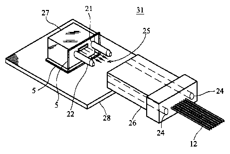
[0017] FIG. 1 shows an optical coupler and converter assembly 31 in a context
of use and
generally in accordance with an illustrated embodiment of the invention.
Included within the
converter assembly 31 may be an optically transparent substrate 5 and optical
array 8 (FIG. 2).
The optically transparent substrate 5 may be attached to a guide pin holder
27. Both the
substrate 5 and guide pin holder 27 may be attached to a common printed
circuit board (PCB) 28.
Transmission paths 25 of the optical array 8 (FIG. 2) pass through the
optically transparent
substrate 5. A.n external waveguide coupler 26 containing optical fibers 12
may be aligned to the
optically clear substrate 5 and the optical array 8.
[0018] The optically transparent substrate 5 may be provided with guide pin
apertures 21.
Guide pin apertures 21 may be laser drilled to relatively close tolerances for
insertion of the
guide pins 22. The external waveguide coupler 26 may contains guide pin
apertures 24 for
receiving guide pins 22 and for aligning the optical fibers 12 to the
transparent substrate 5. The
guide pin apertures 24 and/or guide pins 22 form alignment references fox
coupling the converter
assembly 31 to other optical devices.
[0019] The relatively limited tolerances against lateral misalignment provided
by the
combination of the aperture 21, pin 22 and connector aperture 24 allows for
the precise
alignment of the external waveguide coupler 26 and optical fibers with the
substrate 5. FIG. I
shows guide pins held in place by an accompanying pin holder 27. Thus, the
pins 22 are placed
through the optically transparent substrate 5, and the external waveguide
system 26 is aligned to
the optical array by operation of the substrate 5 which functions as an
alignment substrate that
aligns the transmission paths of the optical array 8 with the transmission
paths of the fibers I2.
[0020] While the optical assembly 31 is shown in the context of converting
between an
electrical signal on the PCB 28 and an optical signal on the fibers 12, it
should be understood
that the converter assembly 31 may be used in any of a number of other
applications. Fox
3
CA 02422986 2003-03-21
WO 02/25341 PCT/USO1/25818
example, the assembly 31 could be coupled electrically to a communication
cable and optically
coupled to another optical array on a circuit board using the guide pins 22
for alignment to form
an electro-optical isolator.
[0021] FIG. 2 shows an optical array 8 containing optical ports 1 (e.g., VCSEL
lasers,
DFB lasers, photodetectors, etc.) with transmission paths 25 extending normal
to the top surface
(i.e., out of the page). Thus, the direction of light is normal to the surface
of interest. The
optical array 8 may be fabricated using conventional techniques.
[0022] t~lso shown on the array 8 are electrical pads 3, electrical traces 2,
and registration
targets 4. The assembly process of the optical array 8 could use registration
targets 4 to
generally locate the position of the optical array 8 on the corresponding
substrate 5 (as described
in more detail below). The electrical traces 2, electrical pads 3, or optical
ports 1 could also be
used as registration targets. The scope of the registration targets is not
limited to one or the
other, but could include a combination of registration targets. For instance,
electrical traces 2
and optical ports 1 could both be used as registration targets 4 in
determining the location of the
optical array 8 on the array substrate 5. In addition to registration targets
4, other alignment
structures and features can also be placed on the surface to further guide the
array 8 into a precise
alignment with the transparent substrate 5. The distances from the
registration targets to the
outer boundaries of the optical device 8 may be programmed into the pick and
place machinery.
Thus, the delivered location of the optical array 8 by the pick and place
machinery is known.
[0023] In order to further guide the array 8 into precise alignment with the
substrate 5, a
series of alignment devices 6, 7 (shown in FIG. 3) may be fabricated on mating
surfaces of the
array 8 and substrate 5. The alignment devices may be fabricated on the same
side of the array 8
as the ports 1. In some cases (described below) the alignment devices may be
fabricated directly
over the ports 1.
[0024] The registration and alignment features 6, 7 on the optical array 8 are
not limited
to any type of material, or any particular location on the surface of the
optical array. The
registration features are not limited to any number either. For instance,
there could be 'm'
optical ports 1, '~' electrical pads 3, and 'o' electrical traces 2, and some
combination used as
registration features.
[0025] The alignment devices 6, 7 may be fabricated using convention
fabrication
technique. FIG. 4 shows a layer 29 of polyimid may be disposed over the mating
surfaces of the
4
CA 02422986 2003-03-21
WO 02/25341 PCT/USO1/25818
array 8 and substrate 5. The layer 29 of polyimid may be any commercially
available
photoreactive material (e.g., 20-100 microns thick) provided with an
associated etching agent.
[0026] A mask may be placed over the polyimid layer on the array 8. The mask
may
transmit (or block) light in areas defining the alignment devices 6, 7. The
mask and layer may
then be exposed and the excess material etched away to leave the devices 6, 7,
shown in FIG. 3.
The devices may be round, square or any other shape.
[0027] Similarly, a mask may be placed over the polyirnid layer 29 disposed on
the
substrate 5. The mask on the substrate 5 may be aligned to the holes 21. Once
aligned to the
substrate 5, the polyimid layer 29 may be exposed and excess material etched
away.
[0028] In general, the alignment devices 6, 7 may be provided as complementary
post
and receptacle type devices (FIG: 4). Posts 6, 7 may be fabricated on the
array 8 and
complementary receptacles 9 may be fabricated on the substrate 5.
Alternatively, any
combination of posts 6, 7 and receptacles 9 may be placed on the array 8 or
substrate, the only
limitation being that any corresponding locations on the array 8 and substrate
S would include a
complementary pair of alignment devices 6, 7 and 9.
[0029] If the registration features (i.e., alignment devices) 7 are optically
transparent,
they can be placed over the active optical regions of the ports 1, as shown in
FIG. 3. When
placed over the optically active regions, the alignment devices 7 have been
found to function as a
lens, directing light along a predictable path through the substrate 5 into
the fibers 12.
[0030] Whether over the active optical region 1 or not, these alignment
structures 6, 7
may have tapered sides of different sizes and profiles that may be used to
guide and align the
optical-component to the mating substrate 5. Alignment features 6 are not
limited to the optical
array 8 though. Coinciding, complementary alignment features 6, 7, 9 can be
placed on the
substrate 5 or on the metal traces 11. The metal traces 11 may be disposed on
the substrate 5 and
used to connect the pads 3 to external connections (e.g., on a supporting
printed circuit board).
Thus, a combination of alignment features 6,7, 9 on both the substrate and
optical array surface
can be used in guiding and aligning the components to their proper location.
[0031] FIG. 4 illustrates the relationship between the alignment features 6, 7
of the
optical array 8 and those corresponding features 9 of the substrate 5. The
structure of the
alignment features 6, 7, 9 functions to guide the optical component 8 into its
correct position on
the substrate 5. The substrate 5 could have built-up sections or removed areas
9, such as guide
CA 02422986 2003-03-21
WO 02/25341 PCT/USO1/25818
pin apertures 21, (see FIG .1), depending on the desired features for the
application. The
substrate 5 could also have on its surface a layer of a polyimid 29 or similar
material. This
material might be easier in manufacturing to a desired shape or form. FIG. 5
illustrates what a
substrate 5 might look like with a polyimid layer 29 between the optical array
8 and the substrate
and with conductive traces partially disposed over the layer 29.
[0032] Alignment features 6, 7 on the substrate 5 or polyimid are not limited
to one side.
They could be located on the surface closest to the optical fiber 12 or on the
surface closest to the
optical array 8. The initial physical placement of the optical components 8
can be done using
standard pick-and-place equipment. Optical alignment occurs as the alignment
features 6, 7, 9
engage and lock into a final position. Tapered edges 18, 19 of the alignment
features allow a
smooth initial placement, and automatic movement into the optical alignment.
[0033] The tapered alignment features (18, 19) of both surfaces can be of
different sizes
in order to complete the alignment process. The tolerances 16 of the pick and
place machine
may be comparable in scope to the operable range of the alignment feature 6,
as shown in FIG. 6.
Otherwise, the initial alignment of the features may not be close enough to
render the tapered
sides functional. Thus, the range of self alignment provided by the alignment
features 6 would
be expected to be larger than the pick and place machinery tolerance 16.
[0034] The tapered surfaces 18, 19 may be shaped using any of a number of
different
methods. Under a first method, the natural process of etching may be used to
control the rate of
taper. Since an etchant would be expected to etch at a constant rate, it would
be expected that a
top of a hole 9 may have a larger diameter than a bottom of the hole.
[0035] Alternatively, the mask used to create the receptacle may have
feathered edges,
thereby increasing an etching rate around a periphery of an entry location of
the hole. By
varying the gradation of the feathering by distance to an edge of the hole 9,
varying degrees of
taper may be achieved.
[0036] The same process used for the receptacles 9 may be applied to the posts
6, 7. For
a more extreme taper, a feathering of the mask may be used to achieve any
desired amount of
taper.
[0037] For example, the diameter of the tip of the post 6, 7 may be
approximately 70
microns. The diameter at the bottom of the receptacle may also be 70 microns.
The taper of the
post 6, 7 may be 45 degrees. The taper of the receptacle may be 45-70 degrees.
6
CA 02422986 2003-03-21
WO 02/25341 PCT/USO1/25818
[0038] If the length of the post 6, 7 and depth of the receptacle are each 70
microns, then
a 45 degree taper within the receptacle 9 would provide an entrance to the
receptacle 9 with a
diameter of approximately three times the diameter of the tip of the post 6,
7. Because of the
taper, the array 8 may be placed at least 70 microns to either side of the
center of the receptacle 9
and still operatively engage the receptacle 9. Alignment would be achieved in
this example
because gravity would cause the tapered post 6, 7 to slide down the tapered
receptacle 9 until the
post 6, 7 reaches the bottom of the receptacle 9. When the post reaches the
bottom of the
receptacle 9, substantially complete alignment would be achieved.
[0039] Further, the taper of the post 6, 7 functions to further shape and
direct optical
transmission. The tapered post 6, 7 may form a frustrum-shaped lens directing
light along an
optical transmission path passing through the substrate 5.
[0040] Many optical components could be placed on the substrate, as shown in
FIG. 4.
Once the critical alignment has been made, the optical arrays 8 may be held in
place by a mass
rapid bonding process. Bonding could include adhesives, solder, stud bumps, or
a similar
material.
[004Ij If the alignment material is transparent such as a polyimid, then the
material can
be modified to form an optical-wavefront transforming structure, as shown in
FIG. S. In this
example, the alignment device is a lens and lens receptacle 9. Such structures
may include, but
are not limited to negative or positive lens, Fresnel lens, or optical guide,
allowing more efficient
coupling of the light between the active optical component I and a light
guiding device such as
an optical fiber 12.
[0042] An optical-wavefront transforming or confining structure, here called
an optical
via (or waveguide) 15, can also be made in the optical transparent substrate
5. In FIG. 7, light is
guided through the area encompassed by the holes 17, normal to the surface of
the page. The
figure illustrates how a system of confining light might look. The apertures
17 in the substrate 5
may be filled with a polyimid, or similar substance having an index of
refraction lower than that
of the substrate's 5. With a lower index of refraction in the apertures 17,
light will be reflected
away from the apertures 17. The apertures 17 would then act as a light
confining structure by
deflecting light towards the center of the circular structure. These apertures
I7 are not limited to
a certain type of filling, but could be left unf'~lled (i.e., filled with
air).
7
CA 02422986 2003-03-21
WO 02/25341 PCT/USO1/25818
[0043] The index of refraction of the substrate 5 could be changed to direct
light as
desired. Material diffusion, compression, or ultraviolet exposure are examples
of methods of
creating an index step in refraction to change a boundary region from guiding
to non-guiding
regions.
j0044] Antireflection coatings and structures can also be used and structured
in the
package to minimize the coupling losses between the active optical components
8 and passive
optical waveguide coupler 26. They may be disposed on the surface of the
substrate 5 nearest to
the optical fiber I2.
j0045] The dielectric material 20 shown in FIG. 8 used for the precision
alignment
structures is placed on the substrate 5. Solder bumps 10, stud bumps, or metal
plating shown in
FIG. 8 on the electrical contact pads 3 may be used to electrically connect
the package traces 2 to
the optical components. These traces can go to other electro-optic components
(not shown).
[004b] Alignment of optical fibers 12 can be determined by alignment apertures
22
through the substrates or by structures built upon the substrate, as shown in
Figure 6. These
features, in turn, may be defined using photolithographic registration targets
4 on the substrate 5
and provide the alignment that is required between the active optical-
component ports 1 and the
optical fiber 12.
[0047] The assembly shown in FIG. 8 can be placed in a housing 23 and sealed,
as shown
in FIG. 9. Guide pins 22 mounted in the housing 23 or guide structures
fabricated on the
transparent substrate 5 will guide the waveguide connector assembly 26 to the
active optical
ports 1.
[0448] Testing or burn-in may be performed on the optical assemblies 31 before
use.
This testing may be done once the optical array 8 has been placed and aligned
(as discussed
above) on some form of substrate 30 to facilitate handling of that component.
These components
may be electrically activated during these procedures, and the optical
characteristics can also be
examined at this time. FIG. 10 illustrates how optical components may be
placed on a large
transparent substrate 30. The substrate 30 may then be placed on a test bed
that has electrical
connections (bed of electrical probes or pads) to electrically activate these
devices. The optical
characteristics of these devices can be accessed through the transparent
substrate 30, which is on
the opposite side of the structure from the electrical interconnects. In this
form, large arrays of
optical assemblies 31 can be simultaneously burned-in and tested before
connection to other
8
CA 02422986 2003-03-21
WO 02/25341 PCT/USO1/25818
devices. After testing, the common substrate 30 is partitioned (cut into
assemblies 31) and the
further packaging can be completed.
(0049] A specifzc embodiment of a method and apparatus for coupling an optical
array to
optical waveguides has been described for the purpose of illustrating the
manner in which the
invention is made and used. It should be understood that the implementation of
other variations
and modifications of the invention and its various aspects will be apparent to
one skilled in the
art, and that the invention is not limited by the specific embodiments
described. Therefore, it is
contemplated to cover the present invention and any and all modifications,
variations, or
equivalents that fall within the true spirit and scope of the basic underlying
principles disclosed
and claimed herein.
9