Note: Descriptions are shown in the official language in which they were submitted.
CA 02423473 2003-03-24
WO 02/27980 PCT/SE01/01990
1
A transmitter circuit comprising a light source and a communi-
cation system
BACKGROUND OF THE INVENTION AND PRIOR ART
The present invention concerns a transmitter circuit comprising a
light source and arranged to operate said light source to transmit
optical communication signals in response to electric input signals
from a first and a second circuit point between which circuit points a
balanced electric input signal is intended to be present. The inven-
tion also concerns a communication system comprising such a
transmitter circuit.
Different transmitter circuits of the above mentioned kind are
known. Such transmitter circuits are often used within telecommuni-
cation systems and data communication systems for transmitting
optical signals in response to electric signals. The optical signals
are usually transmitted in one or more optical fibres. The electric
input signal is usually present as a balanced signal on a pair of
electric conductors, for example on a twisted pair. Such a pair of
electric conductors has a certain characteristic impedance, for ex-
ample 100 ohm. In order to avoid undesired reflections, such a pair
of electric conductors should in its end point be connected to a load
which corresponds to the characteristic impedance.
It should be noted that by a balanced signal is meant that the signal
that is present on the pair of conductors is such that the voltages on
corresponding points on the two conductors are of the same mag-
nitude but have opposite polarity relative to a reference potential.
This reference potential is usually earth potential. With an unbal-
anced signal (or "single-ended") is meant that the signal, i.e. the
voltage variation, is only present on one conductor, while the other
CA 02423473 2003-03-24
WO 02/27980 PCT/SE01/01990
2
conductor, or the reference potential, is at a constant potential,
usually on earth potential.
On a pair of conductors with a balanced signal, due to noise or
other phenomena, a signal which is superposed on the two con-
ductors may occur, a so-called common mode signal, which signal
may vary with time. This signal is often undesired and should
therefore be suppressed. This is often done with the help of, for ex-
ample, transformers, baluns (a balun is a device which converts a
balanced signal to an unbalanced signal) and differential amplifiers.
Also when a balanced electric signal is to be converted to an optical
signal, such an undesired superposed signal need to be suppressed
in order for the light source, which transmits the optical signal, to be
correctly operated. According to the prior art, this has usually been
done by first converting the balanced electric signal to an unbal-
anced electric signal.
Fig. 1 shows an example of the prior art. The electric balanced in-
put signal is here present on a twisted pair 30. The balanced signal
is converted to an unbalanced signal with the help of a balun 41
and a transformer 42. The circuit also comprises a termination re-
sistance 43 which is adapted to the characteristic impedance of the
twisted pair 30. Thereafter follows one or more circuits 44, which
i.a. produce a suitable bias current and a modulation current,
wherein the total current drives the light source 20.
Also EP-A-0 542 480 shows an example of a transmitter circuit. The
transmitter circuit comprises two differentiators and an amplifier for
driving a light emitting diode.
The prior known solutions are relative complicated and expensive,
since they often comprise relatively complicated and expensive
components, such as active components or transformers. Further-
more, known transmitter circuits often have a relatively high current
consumption.
CA 02423473 2003-03-24
WO 02/27980 PCT/SE01/01990
3
It should be noted that by active components is meant components
which produce a gain or a switching, for example transistors, inte-
grated circuits, and diodes.
SUMMARY OF THE INVENTION
An object of the present invention is to achieve a transmitter circuit
which is more simple than typical known transmitter circuits. A fur
ther object is that the transmitter circuit should have a high func
tional reliability and that it should be inexpensive to produce.
These objects are achieved according to the invention with a trans-
mitter circuit of the kind which has been described in the first para-
graph above and which comprises a first circuit branch which ex-
tends from said first point via a third point to at least a fourth point,
and wherein said transmitter circuit comprises a second circuit
branch which extends from said second point via a fifth point to at
least a sixth point, wherein said light source is connected between
said third and fifth points, wherein the components which are posi-
tinned on said first and second circuit branches are chosen such
that the transmitter circuit is formed with a symmetry which is such
that under normal operation conditions a balanced drive voltage is
the case between said third and fifth points, which balanced drive
voltage only depends on the voltage difference between said first
and second points, wherein also the modulation current through the
light source only depends on said voltage difference.
With the invention, the advantage is achieved that the balanced
signal does not need to be converted to an unbalanced signal. The
circuit according to the invention can thereby be realised with sim-
ple and inexpensive components.
ft should be noted that by "normal operation conditions" is meant
that the transmitter circuit works within voltages and currents which
are normal for the transmitter circuit, where, as has been men-
tioned, also an undesired superposed voltage may be present on
the balanced electric signal. However, for example extreme voltage
CA 02423473 2003-03-24
WO 02/27980 PCT/SE01/01990
4
peaks may be considered to constitute non-normal operation condi-
tions.
According to a preferred embodiment of the invention, said first and
second circuit branches are formed with a mirrored symmetry, such
that the electric properties of the components which are arranged
on said first circuit branch correspond to the same electric proper-
ties of the components which are arranged on said second circuit
branch.
This mirrored symmetry may preferably be achieved if the first and
the second circuit branches comprise components with exactly the
same value on corresponding positions in the respective circuit
branch. The feature that the electric properties of the components
correspond to each other means however that it does not have to
be exactly the components on the two circuit branches, as long as
the electric properties of the two circuit branches are the same. For
example, the electric properties which together are the case in the
component or components which are arranged between two nodes
in one of the circuit branches ought to correspond to the same
electric properties which together are the case in the component or
components which are arranged between the corresponding two
nodes in the second circuit branch.
Since the transmitter circuit is formed with this symmetry, it is pos-
sible to, with simple components, maintain a balanced signal all the
way to the light source. Furthermore, it is achieved that the light
source is only modulated by the voltage difference between the
above mentioned first and second circuit points. The current
through the light source is thus independent of a possible common-
mode signal which is present on said first and second circuit points.
According to a further embodiment of the invention, the transmitter
circuit is arranged such that a first constant voltage is the case at
said fourth point and a second constant voltage is the case at said
sixth point. Hereby, a suitable bias-current through the light source
may be obtained in a simple manner.
CA 02423473 2003-03-24
WO 02/27980 PCT/SE01/01990
According to a further embodiment of the invention, the transmitter
circuit is arranged such that at least one of said first and second
constant voltages is adjustable. Hereby, the bias-current may sim
5 ply be adjusted without influencing the modulation current.
According to another embodiment of the invention, the transmitter
circuit comprises a first capacitor arranged on said first circuit
branch between said first and third points and a second capacitor
arranged on said second circuit branch between said second and
fifth points, wherein said first and second capacitors have essen-
tially the same value. Through these capacitors it is in a simple
manner prevented that a direct current, caused by the voltage dif-
ference between said fourth point and said sixth point, is conducted
past the light source. Hereby, the bias-current through the light
source may be determined in a simple manner. Furthermore, energy
is saved since no direct current is conducted past the light source.
According to a further embodiment of the invention, the transmitter
circuit comprises a first resistance on said first circuit branch be-
tween said first and third points and a second resistance arranged
on said second circuit branch between said second and fifth points,
wherein said first and second resistances have essentially the same
value. With the help of these resistances, the relationship between
the voltage of the balanced input signal and the modulation current
through the light source can be adjusted such that a suitable
modulation of the light source is achieved.
According to still another embodiment of the invention, the trans-
, mitter circuit comprises a third resistance arranged on said first cir-
cuit branch between said third and fourth points and a fourth resis-
tance arranged on said second circuit branch between said fifth and
sixth points, wherein said third and fourth resistances have essen-
tially the same value. With the help of these resistances, the volt-
age over the light source is adjusted such that a suitable bias-
current through the light source is obtained.
CA 02423473 2003-03-24
WO 02/27980 PCT/SE01/01990
6
According to a further embodiment of the invention, all components
which are arranged on said first and second circuit branches are
passive components. Hereby, the advantages of the invention are
achieved in a simple manner and with inexpensive components.
Preferably, no transformers or magnetic components are used in
the transmitter circuit. As has been mentioned above, also no balun
is used.
According to another embodiment of the invention, the transmitter
circuit comprises a third circuit branch which extends between a
point on said first circuit branch and the corresponding point on said
second branch, wherein the third circuit branch comprises at least
a fifth resistance which is arranged to function as a termination re-
sistance. The impedance of the circuit may thereby be adjusted to
the characteristic impedance of a pair of conductors which pair
conducts the balanced electric signal to said first and second
points.
According to a further embodiment of the invention, said third circuit
branch comprises a fifth and a sixth resistance which have essen-
tially the same value and which are arranged to together function as
a termination resistance, wherein the transmitter circuit is arranged
such that a third constant voltage is the case between said fifth and
sixth resistances on said third circuit branch. Hereby, a so-called
common-mode termination is achieved, which means that possible
signals which are superposed on both the first and the second cir-
cuit points are terminated, which reduces the occurrence of reflec-
tions and other disturbing phenomena.
According to another embodiment of the invention, the transmitter
circuit comprises transient protection connected to said first and
second circuit branches and arranged to protect the light source
against undesired voltage pulses. The circuit is hereby protected
against, for example, electrostatic discharges.
According to a further embodiment of the invention, the transmitter
circuit comprises a third capacitor arranged on said first circuit
CA 02423473 2003-03-24
WO 02/27980 PCT/SE01/01990
7
branch between said first point and said first capacitor and a fourth
capacitor which has essentially the same value as the third capaci-
tor and which is arranged on said second circuit branch between
said second point and said second capacitor, wherein said third cir-
cult branch extends between a point on said first circuit branch po-
sitioned between said first and third capacitors and a point on said
second circuit branch positioned between said second and fourth
capacitors. With the help of these third and fourth capacitors, the
input signal is AC-coupled. This, together with the above mentioned
third constant voltage and the fifth and sixth resistances, means
that the input signal may be adjusted to end up within an interval, in
which the transient protection works well.
As has been mentioned above, a further object of the invention is to
achieve an advantageous communication system. This purpose is
achieved with a communication system which comprises at least a
pair of electric conductors arranged to conduct a balanced electric
signal, an optical conductor arranged to conduct said signal in opti-
cal form, a transmitter circuit according to any of the preceding em-
bodiments and a receiver unit, wherein said pair of electric con-
ductors is connected to said first and second points, said optical
conductor is arranged to receive and conduct on light from said light
source and said receiver unit is arranged to receive said light from
the optical conductor. The communication system may, of course,
also comprise another transmitter circuit and another receiver unit
arranged to make a bi-directional communication possible in the
communication system.
BRIEF DESCRIPTION OF THE DRAWINGS
Fig. 1 shows a transmitter circuit according to the prior art.
Fig. 2 shows a transmitter circuit and schematically a commu
nication system according to an embodiment of the in
vention.
CA 02423473 2003-03-24
WO 02/27980 PCT/SE01/01990
8
Fig. 3 shows an equivalent circuit of the transmitter circuit ac-
cording to Fig. 2.
Fig.4 shows a transmitter circuit according to another em-
bodiment of the invention.
Fig. 5 shows the principle of preferred embodiments of the in-
vention.
DESCRIPTION OF EMBODIMENTS OF THE INVENTION
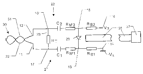
Fig. 2 shows a transmitter circuit and a communication system ac-
cording to the invention. In the shown example, the communication
system comprises a twisted pair 30 of conductors 31, 32. These
conductors are connected to a first 11 and a second 12 point of the
transmitter circuit. It should be noted that other kinds of conductors
than a twisted pair 30 are possible. For example, a ribbon table is
thus conceivable or simply two conductors on a circuit card. A bal-
anced electric input signal is conducted to the first 11 and second
12 points. The transmitter circuit converts this signal to an optical
signal which is transmitted from a light source 20. The communica-
tion system comprises a receiver unit 37 and an optical conductor
35 which conducts light from the light source 20 to the receiver unit
37.
The transmitter circuit has a first circuit branch 21 and a second cir-
cuit branch 22. The first circuit branch 21 extends from the first
point 11 via a third point 13 to a fourth point 14. The second circuit
branch 22 extends from the second point 12 via a fifth point 15 to a
sixth point 16. The light source is connected between the third point
13 and the fifth point 15. The first circuit branch 21 comprises a first
capacitor C~ and a first resistance RM~ which are connected in se-
ries after each other between the first point 11 and the third point
13. In a corresponding manner, the second circuit branch 22 com-
prises a second capacitor C2 and a second resistance RM2 which
CA 02423473 2003-03-24
WO 02/27980 PCT/SE01/01990
9
are connected in series between this second point 12 and the fifth
point 15.
Furthermore, the first circuit branch 21 comprises a third resistance
RBA which is arranged between the third point 13 and fourth point
14. The fourth point 14 is arranged to be at a first constant voltage
VA. In the shown example, this first voltage VA is earth potential.
Furthermore, the second branch 22 comprises a fourth resistance
RB2 which is arranged between the fifth point 15 and the sixth point
16. The transmitter circuit is arranged such that a second constant
voltage VB is the case at the sixth point 16. One of said first VA and
second VB constant voltages may suitably be adjustable. For exam-
ple, the second constant voltage VB may be adjustable. Thereby,
the bias-voltage through the light source 20 may be simply adjusted
without influencing the modulation current.
The transmitter circuit also comprises a third circuit branch 23. This
third circuit branch 23 extends from a point 17 on the first circuit
branch 21 to a point 18 on the second circuit branch 22. On the
third circuit branch 23, a termination resistance RT is arranged. By a
suitable choice of this termination resistance RT, the impedance of
the circuit may be adapted to the characteristic impedance of the
conduction pair 30 which is connected to the transmitter circuit. The
components which are positioned on the first 21 and second 22 cir-
cult branches are chosen such that the transmitter circuit is formed
with a symmetry. The symmetry is such that a balanced drive volt-
age is the case between the third 13 and the fifth 15 points. The
balanced drive voltage is independent of a possible superposed
voltage which is present on the input signal, i.e. on the two first 11
and second 12 points. In this manner, the light source 20 is modu-
lated exactly in response to the voltage difference between the two
conductors 31, 32 which are connected to the first 11 and second
12 points, respectively.
The easiest manner of achieving said symmetry is that the electric
properties of the components which are arranged between different
nodes on the first circuit branch 21 correspond to the same electric
properties of the components which are arranged in corresponding
CA 02423473 2003-03-24
WO 02/27980 PCT/SE01/01990
positions in the second circuit branch 22. This purpose may simply
be achieved if the first capacitor C~ has the same value as the sec
ond capacitor C2, the first resistance RM~ has the same value as the
second resistance RM2, and the third resistance RBA has the same
5 value as the fourth resistance RB2. .
An advantage with the invention is that all components which are
arranged on the respective circuit branch 21, 22 between the first
11 and the fourth point 14 and between the second 12 and the sixth
point 16, respectively, may be passive components. In the shown
10 case, these components consist only of capacitors and resistances.
Hereby, also the use of transformers or more expensive magnetic
components is avoided.
A suitable bias-current through the light source 20 is selected by
the choice of the second constant voltage VB, the third resistance
RBA, and the fourth resistance RB2. The scaling factor between the
voltage of the balanced input signal and the modulation current
through the light source 20 is selected by a suitable choice of the
first resistance RM~ and the second resistance RM2. The first C~ and
the second C~ capacitors prevent a superposed voltage from
reaching the light source 20 in the form of a direct current.
In order to show that the current through the light source 20 is in-
dependent of a possible superposed voltage on the conduction pair
31, 32, reference is made to Fig. 3. Fig. 3 shows an equivalent cir-
cuit of the transmitter circuit according to Fig. 2. As a light source
20, for example a light emitting diode or a laser diode may be used.
A simple model of such a light source 20 is an independent voltage
source VS in series with a resistance RS. ZM~ corresponds to the first
capacitor C~ in series with the first resistance RM~. In a corre-
sponding manner, ZM2 corresponds to the second capacitor C2 in
series with the second resistance RM2. In Fig. 2 also the currents I~,
12, and IS as well as the voltages V~, V~, lJ~, and U2 are marked.
With reference to Fig. 3 the following equations may be formed.
CA 02423473 2003-03-24
WO 02/27980 PCT/SE01/01990
11
II = ~' U'
~MI
Uz=UI+~+Is.Rs (2)
Iz=~ Uz
~M2
Is = VBR Uz + Iz (4)
Is = UI -II (5)
RBI
Since the transmitter circuit is symmetrically formed, also the fol-
lowing equalities are fulfilled.
RB = RBI = RB2
ZM = ZMI = DMZ
With the help of (1 ) to (7), the following expression may be derived.
I (Y-Y)RB-Ts(RB+ZM)+T~BZM
s RB(2ZM + Rs)+ ZMRs
From (8) is clear that the current through the light source only de-
pends on the difference between VZ and V~. If, for example, both V2
and V~ suddenly increase, for example with 100 V, the current
through the light source is not influenced.
In order to determine the bias-current, V2 and V~ may be set to be
equal (V2 = V~). Thereby, the following is derived.
I _ vs(RB + zM)+ vBzM
SB '- RB(~zM + RS)+ ZMRS
CA 02423473 2003-03-24
WO 02/27980 PCT/SE01/01990
12
If it is assumed that ZM is a resistance in series with a capacitor, as
in Fig. 2, then ZM goes towards infinity at the frequency 0 Hz.
Thereby, the following is obtained when ZM goes towards infinity.
(10)
Isa = 2 RB + Rs
The expression (10) thus shows the direct current (the bias-current)
through the light source. The modulation current is the total current
(8) minus the bias-current (9). The modulation current is thus:
~~ - ~)RB 11
Is~u = RB~2zM + Rs~+ zMRs ( J
In order to take a numerical example, it may for example be as
sumed that the light source is a laser with VS = 1.6 V and RS = 30
ohm. Furthermore, it may for example be assumed that VB = +5 V.
If, for example, a bias-current of 8 mA is desired, then the following
is obtained with the help of (10).
RB = 197.5 ohm
If it is assumed that the modulation current should be 1 mA at 1 V
difference between V~ and V2, and if it is assumed that the capaci
tors can be seen as short-circuited at the modulation frequency,
then RM is obtained to the following with the help of (11 ).
RM = 450.8 ohm
It remains to determine RT such that the total impedance matches
the balanced input impedance of the conductor pair. Without RT it is
the case at higher frequencies (ZM = RM), that the input impedance
is the following.
RAN = 2R,~ + 2RB R.Rs
If the obtained numerical values are inserted, then the following is
obtained.
CA 02423473 2003-03-24
WO 02/27980 PCT/SE01/01990
13
RAN = 929.6 ohm
If, for example, a total input impedance of 100 ohm is desired, then
RT gets the value 112.1 ohm.
From the above described example, it is clear that the invention
works as it is intended to work and that the circuit can be dimen
sioned in a simple manner.
Fig. 4 shows another embodiment of the invention. The transmitter
circuit according to Fig. 4 differs from the transmitter circuit ac-
cording to Fig. 2 in that the third circuit branch 23 comprises a fifth
resistance RTE and a sixth resistance RT2. These resistances have
essentially the same value. Furthermore, the third circuit branch 23
is arranged with a third constant voltage V~ between said fifth RTE
and sixth RTE resistances. Furthermore, the transmitter circuit com-
prises a transient protection 27 arranged to protect the light source
20 against undesired voltage pulses. Furthermore, the first circuit
branch 21 of the transmitter circuit comprises a third capacitor C3.
The second circuit branch 22 comprises a fourth capacitor C4. In
order to achieve a suitable symmetry, suitably the third capacitor C3
has the same value as the fourth capacitor C4.
The transient protection 27 may be realised in different manners
known to the person skilled in the art. For example, diodes or zener
diodes may be used in order to limit the voltage if it ends up outside
a certain interval. With the help of the third capacitor C3 and the
fourth capacitor C4, the signal has been AC-coupled before it
reaches the transient protection 27. With the help of the third con-
stant voltage V~ and the fifth RTE and sixth RT2 resistances, it is se-
cured that the input signal is around the third constant voltage V~
which is adjusted to the transient protection 27. It is thereby
achieved that the transient protection 27 only limits the voltage if
non-normal voltages occur. Through the third constant voltage V~
and the fifth RTE and sixth RT2 resistances, also reflections and
other problems are reduced, since a so-called common-mode ter-
mination is achieved which means that signals which are common
to the two conductors are terminated.
CA 02423473 2003-03-24
WO 02/27980 PCT/SE01/01990
14
Fig. 5 shows the principle of the invention. As is indicated with
hatched lines in Fig. 5, the transmitter circuit may comprise further
cross-connections between the first circuit branch 21 and the sec-
ond circuit branch 22. It is even possible that the transmitter circuit
comprises active components. However, preferably passive compo-
nents are used. Concerning the components which are important for
the normal operation of the transmitter circuit, it is preferably the
case that these components are arranged such that the transmitter
circuit is formed mirror-symmetrical along a symmetry line 36 which
passes through the middle of possible cross-connections. Thereby,
the above described advantages of the invention are achieved in a
simple manner. Certain particular components, such as transient
protection, which do not have any influence on the normal opera-
tion, do not necessarily have to be arranged with the mirrored sym-
metry. It should also be noted that the transmitter circuit may com-
prise further components. For example, the transmitter circuit may
be arranged with a low-pass filter for preventing high frequency sig-
nals from reaching the light source.
The invention has several advantages, such as has already been
described above. The input signal does thus not have to be con-
verted into an unbalanced signal. This means i.a. that the voltages
at the points 13 and 15 will be in opposite phases, which means
that disturbances which could reach other components will be small,
since such disturbances from the points 13 and 15 tend to cancel
each other.
A transmitter circuit according to the invention may suitably form
part of a device which is arranged in a home or at a working place
in order to convert electric signals, for example from a computer, to
optical signals which are transmitted via an optical fibre. Such a de-
vice may advantageously be arranged in or in connection to a wall
in a room. The transmitter circuit according to the invention may
also form part of a centrally positioned device which transmits opti-
cal signals to one or more optical fibres in order to transfer these
optical signals to a home or to another place.
CA 02423473 2003-03-24
WO 02/27980 PCT/SE01/01990
The invention is not limited to the shown embodiments but may be
varied within the scope of the following claims.