Note: Descriptions are shown in the official language in which they were submitted.
CA 02423527 2003-03-26
METHOD FOR FORMING MICRO GROOVE STRUCTURE
The present application is based on Japanese Patent
Application No. 2002-84735, the entire contents of which are
incorporated herein by reference.
BACKGROUND OF THE INVENTION
1. Field of the Invention
The present invention relates to a method for forming
a microstructure by dry etching and particularly to a method
for forming a micro groove structure excellent in shape
controllability.
2. Related Art
Optical elements having microstructu~°es
shape-controlled on scales of from the order of microns to the
order of manometers have been developed with the advance of
the field of information communications in recent years.
Functional elements of similar microstructures have been
developed also in the biotechnological and medical field as
well as the information communication field.
At present, lithography technology is a typical
micromachining technique. This is a technique for forming a
micro concavoconvex shape in a substrate material by etching
after forming a desired pattern by irradiating a photosensitive
r esist with energy wave such as u1 traviolet rays, electron beams
or X-rays and masking the substrate material with the resist
per se or transferring the pattern onto a high durable material
1
CA 02423527 2003-03-26
such as metal and masking the substrate material with the high
durable material.
On the other hand, sophisticationofthemicroshapeformed
in the substrate, increase of the aspect ratio in the
concavoconvex shape, diversification of the material to be
etched, etc. are required of an etching technique. Dry etching
using plasma has begun to be frequently used as a technique
which meets such requirements of more accurate etching.
As the mask pattern is sophisticated and made micro as
described above, abrasion of the masking material at etching,
however, becomes an issue. particularly when a deep groove
needs to be formed in the substrate, there occurs a problem
that the groove depth allowed to be etched is decided by abrasion
of the masking material.
Although improvement of selective ratio indicating the
etching speed ratio between the masking material and the
substrate material can be achieved to a certain degree by
selection of the masking material, etching gas, plasma condition,
etc., the improvement achieved has a limit when it depends on
physical and chemical properties of the material.
Although the durability of the mask can be improved when
the mask per se is made thick, the mask needs to be patterned
by photolithography or the like in advance. The mask allowed
to be machined from a photo resist finite in thickness has a
limit in thickness. In addition, provision of the mask as a
L
CA 02423527 2003-03-26
thicker film than. required brings a problem that micro pattern
accuracy is spoiled.
SUMMARY OF THE INVENTION
The invention is developed to solve these problems and
an obj ect of the invention is to provide a method for forming
a micro groove structure by dry etching without any limit due
to the durability of a mask.
A method of forming a micro groove structure according
to the invention has the steps of : (a) forming a mask pattern
on a substrate capable of being subjected to dry etching; (b)
dry etching the substrate having the mask pattern formed thereon;
(c) vapor-phase forming a thin film of a masking material for
the dry etching, on a non-etched sur face portion of the substrate
after the dry etching; and (d) dry etching the substrate having
the thin film formed thereon. The steps (a) to (d) are carried
out successively.
Incidentally, the above "non-etched surface portion of
the substrate" is not limited to a surface of the substrate
which was masked in the step (a) so as to form the mask pattern
and exposed by the abrasicn of the mask in the dry etching of
the step (b) , but it may include a surface of the mask. pattern
remained after performing the dry etching of the step (b).
Preferably, after the steps (a) to (d) are carried out
successively, the steps (c) and (d) are repeated successively
one or mcre times . This repetition makes it possible to form
3
CA 02423527 2003-03-26
each groove having a higher aspect ratio. The term "aspect
ratio" means the ratio of the depth of the groove to the width
of the groove.
Because a mask is formed again after dry etching is carried
out to a certain degree, additional etching can be repeated
any number of times. Accordingly, a desired micro groove
structure can be formed without any limit due to abrasion of
the mask.
Preferably, in the step (c) carried out initially and
the step (c) repeated afterwards, particles forming the thin
film are obliquely deposited on the substrate.
Accordingly, the maskir_g material can be prevented from
being depos i ted on a bottom o f each micro groove during machining
when the mask is formed again. There is no hindrance to
additional etching.
Preferably, inductive coupling plasma reactive ion
etching is used as the dry etching in the steps (b) and (d).
Further, when the mask pattern formed in the step (a)
is a pattern of straight lines periodic in one direction or
in two directions in a plane of the substrate, a periodic micro
concavoconvex structure can be formed.
Further, when the method for forming the micro groove
structure is applied to a substrate having a multilayer film
structure, a two-dimensional or three-dimensional periodic
structure can be formed.
4
CA 02423527 2003-03-26
BRIEF DESCRIPTION OF THE DRAWINGS
Figs. 1A to 1D are views for explaining the groove
formation steps of the invention;
Fig. 2 is a view for explaining oblique film-farming;
Fig. 3 is a typical view showing an oblique film-forming
method according to the invention;
Fig. 4 is an enlarged typical view of a portion in which
a groove is formed; and
Figs. 5A and 5B are views showing external appearance
of photonic crystal formed as an embodiment of the invention.
DETAILED DESCRIPTION OF THE PREFERRED EMBODIMENTS
An embodiment of the invention wil l be described below
in detail with reference to the drawings . Figs . 1A to 1D are
conceptual views showing the invention.
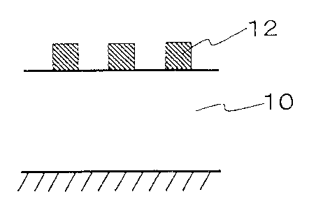
F,~.rst, a thin film of a masking material having a
predetermined thickness is formed on a surface of a substrate
20 to be etched, and subjected to a method such as
photolithography to thereby form a mask pattern of a desired
masking material 12 (Fig. iA).
First, aphoto resist is appliedor~a surface of a substrate.
The photo resist is exposed to light while a photo mask of a
desired pattern is used. The photo resist is developed so that
a mask pattern due to the photo resist is formed.
As occasion demands, a mask of a metal such as chromium,
nickel or titanium or a mask of an inorganic materi al such as
r
CA 02423527 2003-03-26
silica or t.tania can be also used. In each of these cases,
a pattern is formed in the same manner as described above: after
a film of the masking material is formed on the substrate and
a photo resist or the like is applied on the film. There, while
the photo resist or the like is used as a mask, the masking
material is etched to form opening portions.
Alternatively, a lift-off method may be used. The method
is a method of forming a mask pattern by the steps of: forming
a filmof amaskingmaterial on a photo resist formed as a reversal
pattern; and removing the photo resist. The method can be
effective) y applied to a masking mater ial such as precious metal
which is hard to be etched.
Although a 1 traviol et irradiation is generally used for
exposing the photo resist to light, electron beam writing or
X-ray exposure is suitable for forming a more micro pattern.
The invention can be applied even when any method and
any masking material are used.
A first-time etching process is performed for a
predetermined time in the condition that this mask is used.
The time is decided so that the mask pattern is not deteriorated
due to abrasion (12a) of the masking material 12 by etching.
Dry etching is used as the etching. 1'he reason why dry
etching is used is based on the shape controllability thereof .
In wet etching, liquid goes to the back of the masking material
because of the isotropic property thereof. Although the
6
CA 02423527 2003-03-26
property may be ignored when the shape is etched i n the order
of microns in the condition that the aspect ratio is not required,
the property becomes a significant issue as the etching scale
is reduced from the order of microns to the order of sub-microns
or manometers . When a material such as crystal per se having
anisotropy is used, directional etching can be made but the
substrate material is limited to such a material.
On the other hand, in dry etching, directivity can be
given tc a process when an external :Meld such as an electric
field is operated because gas such as ionized gas having electric
charge is mainly used as etching gas. Dry etching is classified
into a physical method such as ion beam etching or laser ablation
and a method using chemical reaction such as reactive ion etching
(RIE) .
Particularly, reactive ion etching is a process which
is effective for materials to be etched because a gas reactive
to a material to be etched can be selected so that etching can
be made by using various mixed gases . Especially, inductive
coupling plasma reactive ion etching (ICP-RIE) is promising
from the point of view or ir_crease in etching rate and increase
in etching area because plasma can be generated densely and
stably. Moreover, ICP-RIE can prevent the substrate from being
damaged because the substrate is not exposed t;o plasma compared
with tr:e general opposed type RIE.
In addition, when fluorocarbon gas is introduced, a carbon
7
CA 02423527 2003-03-26
polymer film can be deposited en an un-etched portion to thereby
control the directivity of etching. That is, when etching is
performed while a polymer film is formed on a side wall of each
groove at the time of formation of grooves, the grooves can
be formed as high-aspect-ratio grooves. According to this
method, each groove can be made deep in proportional to the
etching time. Because the etching time is however a time in
which the masking material is present, it is unchanged that
the durability of the masking material is sigr:ificant as
described above in the related art. In any case, it is important
to select amethod adapted to the substrate material to be etched.
By any one of these methods, grooves 20 each having a side surface
substantially perpendicular to a surface of the substrate can
be formed (Fig. 1B).
Then, a second-time mask-forming process is applied to
a portion 10a of the substrate surface which has been not etched
yet. On this occasion, an idea is required so that t:ne masking
material is not deposited on the inside of the etched groove
20 portion (Fig. 1C) . It is therefore preferable that a film
of the masking material is farmed in a direction inclined to
the substrate.
Here, on the surface of the portion 10a cf the substrate
surface which has been not etched, it is not necessary that
the masking material is completely removed. The second-time
mask-forming prccess can be performed on the masking material
8
CA 02423527 2003-03-26
formed in the first-time mask-forming process.
A vacuum evaporation apparatus or a sput tering apparatus
can be used for forming a metal mask film. Various kinds of
sputtering apparatuses such as facing target sputtering, ion
beam sputtering, helicon sputtering, etc. may be used as the
sputterir_g apparatus. The film-forming tendency varies
according to the configuratian of the apparatus.
The directivity of the film-forming component is
important to the invention. The film-forming mode is roughly
classified into a mode in which the film-forming component
reaches the substrate straightly (with directivity) and a mode
in which the film-forming component reaches the substrate in
all directions (without directivity). The relation between
the film-forming directivity and the pattern of the material
to be etched needs to be considered so that the masking material
can be prevented frombeing deposited on the portion to be etched.
If film-forming is performed perpendicularly to the
substrate surface in the condition that film-forming is
performed with directivity, it is a matter of course that the
maskingmaterial is deposited on the i.-zside of each groove etched
initially. This problem can be solved when the film is formed
obliquely on the substrate in which grooves have been already
formed to a certain degree by initial etching. Specifically,
when film-forming is performed in the condition that the
substrate 10 is inclined at an angle 6 to the direction of a
9
CA 02423527 2003-03-26
film-forming particle beam 30 as shown in Fig. 2, the masking
material can be prevented from being deposited on the inside
of each of grooves in the patterned portion 24.
On the other hand, when film-forming is performed without
directivity, a film-forming effect can be obtained to a certain
degree by oblique f i1m-forming but the masking material is still
unavoidably deposited on the portion to be etched because of
the perpendicular component of the masking material. The
degree of deposition, however, depends on 'the groove structure
formed by initial etching.
In such a case, a baffle 32 -nay be placed in front of
the patterned portion 24 having an etched groove portion as
shown in Fig. 3 so that the film-forming component perpendicular
to the substrate 10 surface can be removed to perform only oblique
film-forming. The angle of incidence of the oblique
film-forming component can be decided on the basis ef the
distance between the substrate 10 surface and the baffle 32
and the size of the baffle 32.
In any case, the maximum angle a (Fig. 4) at which the
film-forming component reaches the portion to be etched and
the minimum angle 8 of incidence of the film-forming component
is selected to satisfy the relation a < 8 roughly. Conversely,
when the inclination angle of the substrate or the size of the
baffle and the distance between the substrate and the baffle
are adjusted in consideration of the depth of each of the grooves
CA 02423527 2003-03-26
20 formed by the first-time etching process, the mask-forming
range can be controlled to the optimum.
When a second-time etching process is then performed,
high-aspect-ratio grooves 22 which could not be achieved because
of poor durability of the masking material in the related art
can be formed (Fig. 1D) . This means that grooves can be formed
even in the case where the substrate material. is very slow ir~
etching rate, that is, poor in selective ratio with respect
to themaskingmaterial . For example, deep grooves can be formed
even in a s tructure such as a periodic line pattern in the scale
of the order of sub-microns, which is severe in abrasion because
of the large specific surface area of the mask.
When regeneration of the mask and etching after the
regeneration of the mask are repeated alternately, the problem
that desired etching cannct be made because of shortage of
durabi'_ity of the mask can be solved theoretically. If there
is a hindrance to patterning accuracy when the mask is made
thick at the time of regeneration of the mask, the number of
repeated regeneration of the mask and etching may be increased
while etching in the fourth step (d) is performed for a short
time so that etching can be made with higher accurate.
(Example)
An example of a micro groove structure formed in a
dielectricmuitilayer filmbyamethodaccordin.gto the invention
will be described below.
l
CA 02423527 2003-03-26
A multilayer film (of 20 layers each having a thickness
of310nm) in which silica (SiO~) and titania (TiO~) were laminated
alternately on a silica glass substrate by vacuum vapor
deposition was used as a substrate material.
First, a resist was patterned. After the mul tilayer film
substrate was spin-coated wi th an electron beam resist (ZEP520
made by Zeon Corp. ) about 0.5 um thick, the electron beam resist
was baked in an oven at 180°C for 20 minutes. The electron
beam resist was spin-coated with an antistatic agent (ESPACER
3002 made by Showa Denko K.K. ) about 50 nm thick. An electron
beam writing apparatus (ELS5700 made by Elion:ix Inc. ) was used
for performing writing, se that a linear pattern with a line
width of 0.5 um was formed.
On the sampl a subjected to patterning, a film of chromium
about 100 nm thick was formed by a sputtering apparatus ( facing
target sputtering apparatus made by Osaka Vacuum, Ltd.) with
chromium as a target. Then, the mask pattern. was transferred
and formed by a lift-off method. An inductiVE' coupling plasma
reactive ion etching apparatus (RIE-200IP made by SAMCO
International, Irc.) was used for etching. Etching was
performed for l5minuteswhileCjF~andargonwereusedas reactive
gases in plasma. The depth of the groove formed in this case
was about 2 . 4 um. The aspect ratio was about 5 . On this occasion,
the chromium mask deteriorated to a nearly critical point.
After this sample was attached to the sputtering apparatus
12
CA 02423527 2003-03-26
again, a baffle was provided in the apparatus so as to be far
by 5 mm from an upper surface of the substrate. The baffle
was a rectangular stainless plate with a size of 5 X 20 mm and
a thickness of 0 . 5 mm. The baffle was disposed so that 20 mm-long
sides were parallel to the lengthwise direction of the line
pattern formed on the substrate. A film of chromium was formed
for 25 minutes to thereby regenerate the mask. On this occasion,
a film of chromium about 200 nm thick was formed on each convex
top portion of the pattern. Etching was performed again for
20 minutes by the etching apparatus.
Fig. 5A shows a photograph as a result of etching. Fig.
5B is a typical view of the etching resul t . When periodic grooves
22 were formed in the multilayer fil.m~ 15, a two-dimensional
periodic structure 100 could be formed. This structure
functioned as so-called photonic crystal. OT1 this occasion,
the depth of each groove reached tc 4.5 um and the aspect: ratio
was about 9 when the width of the groove was 0.5 um.
According to the invention, a high-aspect-ratio groove
structure which could not be formed by dry etching because of
shortage of durability of a masking material in the related
art can be achieved when both regeneration of a mask and etching
are repeated in a process.
13