Language selection

Search

Patent 2424101 Summary

Third-party information liability

Some of the information on this Web page has been provided by external sources. The Government of Canada is not responsible for the accuracy, reliability or currency of the information supplied by external sources. Users wishing to rely upon this information should consult directly with the source of the information. Content provided by external sources is not subject to official languages, privacy and accessibility requirements.

Claims and Abstract availability

Any discrepancies in the text and image of the Claims and Abstract are due to differing posting times. Text of the Claims and Abstract are posted:

  • At the time the application is open to public inspection;
  • At the time of issue of the patent (grant).
(12) Patent: (11) CA 2424101
(54) English Title: EFFICIENTLY GENERATING SELECTABLE ANTENNA POLARIZATION
(54) French Title: PRODUCTION EFFICACE D'UNE POLARISATION D'ANTENNE SELECTIONNABLE
Status: Deemed expired
Bibliographic Data
(51) International Patent Classification (IPC):
  • H01Q 13/02 (2006.01)
  • H01Q 3/26 (2006.01)
  • H01Q 15/24 (2006.01)
  • H01Q 21/24 (2006.01)
  • H03F 1/32 (2006.01)
  • H04B 7/10 (2017.01)
  • H04L 27/36 (2006.01)
(72) Inventors :
  • MALONE, HUGH ROBERT (United States of America)
  • FULLER, RONALD DEE (United States of America)
(73) Owners :
  • CDC PROPRIETE INTELLECTUELLE (France)
(71) Applicants :
  • MOTOROLA, INC. (United States of America)
(74) Agent: GOWLING WLG (CANADA) LLP
(74) Associate agent:
(45) Issued: 2010-04-13
(86) PCT Filing Date: 2001-10-10
(87) Open to Public Inspection: 2002-04-18
Examination requested: 2006-06-20
Availability of licence: N/A
(25) Language of filing: English

Patent Cooperation Treaty (PCT): Yes
(86) PCT Filing Number: PCT/US2001/042633
(87) International Publication Number: WO2002/031917
(85) National Entry: 2003-03-28

(30) Application Priority Data:
Application No. Country/Territory Date
09/687,361 United States of America 2000-10-13

Abstracts

English Abstract


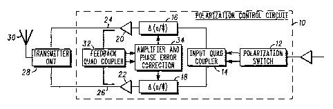
An antenna system (10) capable of transmitting electromagnetic radiation using
the technique of combining two quadrature signals for either right hand
circular polarization or left hand circular polarization using a circularly
polarized antenna (30), or alternately, either horizontal or vertical
polarization using a linearly polarized antenna (36) while incorporating
feedback for automatically correcting for amplitude and phase variations in
the quadrature paths using a switch (12) which selects the sense of the
polarization and electronic optimization of the transmit antenna (30, 36). The
antenna system includes a control circuit having a polarization switch (12)
for receiving a transmission signal. The switch (12) generates first and
second output signals which are substantially similar to the transmission
signal, and determines whether to apply the transmission signal to one of a
first or a second switch output. A coupler (14) receives the first and second
switch outputs and generates first and second output signals having a
predetermined phase difference. A variable detector (16, 18) detects and
adjusts a relative amplitude and phase of the respective first and second
output signals. An error correction circuit (34) determines an adjustment to
the variable phase detector to vary the phase and amplitude of the first and
second output signals in accordance with the relative amplitude and phase of
the respective first and second output signals.


French Abstract

Cette invention se rapporte à un système d'antenne (10), qui est capable de transmettre un rayonnement électromagnétique en utilisant une technique qui consiste à combiner deux signaux en quadrature soit pour une polarisation circulaire droite soit pour une polarisation circulaire gauche au moyen d'une antenne polarisée circulairement (30) ou, dans une variante, soit pour une polarisation horizontale soit pour une polarisation verticale au moyen d'une antenne polarisée linéairement (36), tout en incorporant la rétroaction pour permettre la correction automatique des variations d'amplitude et de phase dans les voies en quadrature au moyen d'un commutateur (12) qui sélectionne le sens de la polarisation et l'optimisation électronique de l'antenne de transmission (30, 36). Ce système d'antenne comprend un circuit de commande ayant un commutateur de polarisation (12) destiné à recevoir un signal de transmission. Le commutateur (12) produit un premier et un second signal de sortie qui sont essentiellement similaires au signal de transmission et il détermine s'il faut appliquer le signal de transmission à la première ou à la seconde sortie du commutateur. Un coupleur (14) reçoit les première et seconde sorties du commutateur et produit un premier et un second signal de sortie ayant une différence de phase prédéterminée. Un détecteur variable (16, 18) détecte et ajuste une amplitude et une phase relatives des premier et second signaux de sortie respectifs. Un circuit de correction d'erreurs (34) détermine un ajustement à apporter au détecteur de phase variable, pour faire varier la phase et l'amplitude des premier et second signaux de sortie en fonction de l'amplitude et de la phase relatives des premier et second signaux de sortie respectifs.

Claims

Note: Claims are shown in the official language in which they were submitted.


-6-

CLAIMS

What is Claimed is:

1. An antenna polarization control circuit, the antenna polarization control
circuit receiving a transmission signal, comprising:

a polarization switch for receiving the transmission signal, the polarization
switch generating a first and second output signal, each first and second
output signal
being substantially similar to the transmission signal, the polarization
switch having a
first switch output and a second switch output, where the polarization switch
selects
whether to apply the transmission signal to the first switch output or the
second switch
output;

a coupler, the coupler having first and second inputs respectively connected
to
the first and second switch outputs, the coupler having first and second
coupler
outputs, the coupler generating a first output signal for output on the first
coupler
output and a second output signal for output on the second coupler output,
wherein
the first and second output signals have a predetermined phase difference;

a variable detector for detecting and adjusting relative amplitude and phase
of
the first and second output signals; and

an error correction circuit for determining an adjustment to the variable
detector to vary phase and amplitude of the first and second output signals in
accordance with the relative amplitude and phase of the first and second
output
signals.

2. The antenna polarization control circuit of claim 1 wherein the variable
detector further comprises:

a first variable detector for receiving and adjusting the first output signal
and
generating a first baseline signal; and

a second variable detector for receiving and adjusting the second output
signal
and generating a second baseline signal.


-7-


3. The antenna polarization control circuit of claim 2 further comprising a
baseline coupler for receiving at least a portion of the first baseline signal
and at least
a portion of the second baseline signal, the baseline coupler generating a
first
coupled signal and a second coupled signal for input to the error correction
circuit.

4. The antenna polarization control circuit of claim 2 further comprising an
output coupler for receiving the first baseline signal and the second baseline
signal,
the output coupler generating first and second coupled baseline output
signals.

5. The antenna polarization control circuit of claim 4, wherein the first and
second output signals are output to a transducer, the transducer combining the
first
and second output signals to generate an antenna signal.

6. The antenna polarization control circuit of claim 1 wherein the coupler
generates one of the first and second coupler outputs to a first polarization
and an
opposite polarization to another of the first and second coupler outputs in
accordance
with a selection of the polarization switch.

7. The antenna polarization control circuit of claim 6 wherein the opposite
polarization is selected from one group of right hand circular polarization
and left hand
circular polarization.

8. The antenna polarization control circuit of claim 6 wherein the opposite
polarization is selected from the group of horizontal polarization and
vertical
polarization.

9. An antenna system comprising:

a polarization switch, the polarization switch having an input for
receiving an input signal and a first and second switch output, the
polarization switch
selecting one of the first and second switch outputs for receiving the input
signal;

an input coupler, the input coupler having a first input and a second
input for generating respective first and second input coupler signals,
wherein the first
and second input coupler signals have a predetermined phase difference, the
first


-8-


switch output of the polarization switch connected to the first input of the
input
coupler, the second switch output of the polarization switch connected to the
second
input of the input coupler;

a first amplitude and phase variable detector, the first amplitude and
phase variable detector receiving as an input the first input coupler signal,
the first
amplitude and phase variable detector generating a first baseline signal;

a second amplitude and phase variable detector, the second amplitude
and phase variable detector receiving as an input the second input coupler
signal, the
second amplitude and phase variable detector generating a second baseline
signal;

an error correction circuit, the error correction circuit receiving the first
and second baseline signals, the error correction circuit generating control
signals to
vary the first and second baseline signals of the first and second amplitude
and phase
variable detectors;

a transducer, the transducer receiving the first and second baseline
signals and generating an antenna signal; and

an antenna, the antenna having an input port receiving the antenna
signal.

10. The antenna system of Claim 9 wherein the antenna is a circularly
polarized antenna.

11. The antenna system of Claim 10 wherein the input coupler is a 3dB
coupler.

12. The antenna system of Claim 9 wherein the input coupler is a 3dB
coupler.

13. The antenna system of Claim 9 wherein the antenna is a linearly
polarized antenna.


-9-


14. An antenna polarization control circuit comprising:

a switch, the switch have an input and a first output and a second
output, for selecting an antenna polarization;

an input coupler, the input coupler having a first input and a second
input and a first output and a second output, the first and second outputs
separated in
phase by 90 degrees, the first output of the switch connected to the first
input of the
input coupler, the second output of the switch connected to the second input
of the
input coupler, for facilitating an antenna polarization;

a first amplitude and phase variable element, the first amplitude and
phase variable element having an input, a variable input, and an output, the
first
output of the input coupler connected to the input of the first amplitude and
phase
variable element;

a second amplitude and phase variable element, the second amplitude
and phase variable element having an input, a variable input, and an output,
the
second output of the input coupler connected to the input of the second
amplitude and
phase variable element;

a first amplifier, the first amplifier having an input and an output, the
output of the first amplitude and phase variable element connected to the
input of the
first amplifier;

a second amplifier, the second amplifier having an input and an output,
the output of the second amplifier and the second amplitude phase variable
element
connected to the input of the second amplifier;

a second coupler, the second coupler having an input, an output, and a
sampling output, the output of the first amplifier connected to the input of
the second
coupler, the second coupler generating a second coupled signal at said output
of the
second coupler;

a third coupler, the third coupler having an input, an output, and a
sampling output, the output of the second amplifier connected to the input of
the third
coupler, the third coupler generating a third coupled signal at said output of
the
second coupler;

an isolation switch, the isolation switch having a first input and a second
input and a first output and a second output, the first and second outputs
separated in
phase by 90 degrees, the sampling output of the second coupler connected to
the first


-10-


input of the isolation switch, the sampling output of the third coupler
connected to the
second input of the isolation switch, the isolation switch generating feedback
error
signals;

amplitude and phase error correction circuitry, the amplitude and phase
error correction circuitry having a first input and a second input and a first
output and
a second output, the first input of the amplitude and phase error correction
circuitry
connected to the first output of the isolation switch, the second input of the
amplitude
and phase error correction circuitry connected to the second output of the
isolation
switch, the first output of the amplitude and phase error correction circuitry
connected
to the variable input of the first amplitude and phase variable element, the
second
output of the amplitude and phase error correction circuitry connected to the
variable
input of the second amplitude and phase variable element;

a fourth coupler, the fourth coupler having a first input and second input
and a first output and second output, the first and second outputs separated
in phase
by 90 degrees, the first input of the fourth coupler receiving the second
coupled
signal, the second input of the fourth coupler receiving the third coupled
signal, said
fourth coupler recombining the outputs of the first and second amplifiers to
produce a
first transducer input signal and second transducer input signal;

an ortho-mode transducer receiving the first transducer input signal and
the second transducer input signal, the ortho-mode transducer having a first
input, a
second input, and an output, the ortho-mode transducer generating an antenna
signal
from the first transducer input signal and the second transducer input signal;
and

an antenna, the antenna having an input port, the input port receiving
the antenna signal.

15. The antenna polarization control circuit of Claim 14 wherein the antenna
is a circularly polarized antenna.

16. The antenna polarization control circuit of Claim 14 wherein the input
coupler is a 3dB coupler.

17. The antenna polarization control circuit of Claim 14 wherein the isolation
switch is a 3dB coupler.


-11-


18. The antenna polarization control circuit of Claim 14 wherein the antenna
is a linearly polarized antenna.

19. The antenna polarization control circuit of Claim 14 wherein the fourth
coupler is a 3dB coupler.


Description

Note: Descriptions are shown in the official language in which they were submitted.


CA 02424101 2003-03-28
WO 02/31917 PCT/USO1/42633
-1
EFFICIENTLY GENERATING SELECTABLE ANTENNA POLARIZATION
BACKGROUND OF THE INVENTION
Field of the Invention
This invention relates to an antenna system capable of transmitting
electromagnetic radiation and, more particularly, to microwave transmitters
associated with an antenna which allows the user to select antenna
polarization.
Background Information
It is known in the radio frequency (RF) field that feeding two linearly
polarized
antenna elements with quadrature signals yields circular polarization. It is
also known
that operating on the relative phase of each of these signals changes the
sense of the
circular polarization. This technique is generally limited to radar and
jamming
applications where the amount of cross-polarization signal is less important.
However, in the field of communications, dual polarization is often used to
increase
the number of independent signals that can share a common spectrum. Therefore,
for communication applications, it becomes critical to minimize the level of
the cross
polarized signal to facilitate the maximum number of independent signals.
The conventional method for generating high quality switchable dual
polarization is to use an antenna with two input ports, one for each of the
desired
polarizations. An RF switch is then used to connect to the appropriate input
port of
the antenna, thus allowing selection of the desired polarization. Also, in
order to meet
the output power requirements of many implementations, several amplifiers must
be
used. As a result, one or more couplers are required for combining the outputs
of
multiple amplifiers. One must also keep in mind that the RF switch which is
selected
must be capable of switching the full output power of these amplifiers. In
light of this,
3o it is desirable to eliminate the need for high power switching and
couplers, reducing
the amplification required to overcome the losses inherent in these devices.
Finally, it
is desirable to alternately utilize a quadrature coupler for recombining
quadrature
signals, allowing application to linearly polarized antenna systems.


CA 02424101 2003-03-28
WO 02/31917 PCT/USO1/42633
-2-
BRIEF DESCRIPTION OF THE DRAWINGS
The present invention will hereinafter be described in conjunction with the
appended drawing figures, wherein like numerals denote like elements, and:
Figure 1 is a schematic diagram showing a system embodying the invention;
Figure 2 is a schematic diagram showing the circularly polarized antenna
implementation in accordance with a preferred embodiment of the present
invention;
and
Figure 3 is a schematic diagram showing the linearly polarized antenna
implementation.
DETAILED DESCRIPTION OF THE PREFERRED EXEMPLARY EMBODIMENTS
The ensuing detailed description provides preferred exemplary embodiments
only, and is not intended to limit the scope, applicability, or configuration
of the
invention. Rather, the ensuing detailed description of the preferred exemplary
embodiments will provide those skilled in the art with an enabling description
for
implementing a preferred exemplary embodiment of the invention. It being
understood that various changes may be made in the function and arrangement of
elements without departing from the spirit and scope of the invention as set
forth in
the appended claims.
This technique for efficiently generating selectable antenna polarization
incorporates a circuit for combining two quadrature signals to obtain circular
polarization, and adds a simple feedback method to correct for amplitude and
phase
errors in the signal paths thus minimizing the level of the cross-polarized
signal. As
additional benefits, the invention eliminates the insertion loss introduced by
a
polarization switching device, the difficulty in realizing solid state
switches for
application requiring more than 100 watts of output power, and the need for an
expensive polarizator on the output of the antenna, and improves the
reliability since
the power amplifier failure rate is nearly proportional to the output power
requirement
of the amplifier while reducing the overall cost of the implementation.
Referring now to Figure 1, an expanded RF block diagram for the outdoor unit


CA 02424101 2003-03-28
WO 02/31917 PCT/USO1/42633
-3-
(ODU) is shown wherein the polarization control circuit 10 is contained in the
shaded
area. Thus, the invention is incorporated in the design of a larger
communication
system.
Referring now to Figure 2, a polarization control circuit 10, as contained in
the
shaded area in Figure 1, is shown in accordance with a preferred embodiment of
the
present invention. More specifically, Figure 2 discloses the polarization
control circuit
for the circularly polarized antenna implementation of the invention. The
forward
signal path consists of polarization switch 12, input quadrature coupler 14,
which may
be a 3 decibel (dB) coupler, amplitude and phase variable elements 16, 18,
power
10 amplifiers 20, 22, couplers 24, 26, ortho-mode transducer junction also
known as an
ortho-mode tees, or dual-mode transducer 28, and a circularly polarized
antenna 30.
The input signal is applied to polarization switch 12 which allows either
right hand
circular polarization (RHCP) or left hand circular polarization (LHCP) by
selecting the
input port of the input quadrature coupler 14 to which the input signal is
connected.
The outputs of input quadrature coupler 14 are in turn connected to amplitude
and
phase variable elements 16, 18 which provide the baseline quadrature signals
to the
inputs of power amplifiers 20, 22 respectively. The outputs of power
amplifiers 20, 22
feed two linearly polarized input ports of an ortho-mode transducer 28 through
couplers 24, 26. The output of ortho-mode transducer 26 is then connected to
circularly polarized antenna 28.
Feedback paths around power amplifiers 20, 22 consist of couplers 24, 26,
feedback quadrature coupler 32, which may be a 3dB coupler, and amplitude and
phase error correction circuitry 34, and amplitude and phase variable elements
i 6,
18.
The operation of this feedback system will now be described in connection with
a particular non-limiting example. A sample of the baseline quadrature signal
which
has been amplified by power amplifiers 20, 22 is taken from the output of
power
amplifiers 20, 22 by couplers 24, 26 and feed into feedback quadrature coupler
32.
Feedback quadrature coupler 32 then provides these signals to amplitude and
phase
error correction circuitry 34. Amplitude and phase error correction circuitry
34 then
processes these signals generating vector error signals which contain the
representative amplitude and phase information denoting the deviation from the
baseline quadrature signal introduced by power amplifiers 20, 22 in the
amplification


CA 02424101 2003-03-28
WO 02/31917 PCT/USO1/42633
-4-
process. These vector error signals are then applied to amplitude and phase
variable
elements 16, 18 where they are vectorially added to the baseline quadrature
signal
which were applied to the inputs of power amplifiers 20, 22 from input
quadrature
coupler 14. Thus, the feedback compensates for variations in amplitude or
phase
introduced into the forward path by power amplifiers 20, 22. This then ensures
that
the two linearly polarized antenna input ports of ortho-mode transducer 28 are
fed
with equal amplitude signals that differ only in phase by 90 degrees. In other
words,
this feedback insures that a minimum signal level is obtained from one of the
coupler
outputs while a maximum signal level is obtained from the other depending upon
1 o which polarization is desired. Therefore, the polarization control circuit
10 for the
circularly polarized antenna implementation of the invention allows the use of
a
technique in the field of communications which was generally limited to radar
and
jamming applications since the level of the cross polarized signal is
minimized while
allowing the maximum number of independent signals.
Having described the functionality, it is important to point out some addition
benefits of polarization control circuit 10 for the circularly polarized
antenna
implementation of the invention. Since the conventional method for generating
high
quality switchable dual polarization is to use an antenna with two independent
ports
and an RF switch to select the appropriate port, problems associated with the
RF
switch are encountered, as will be described next. First, the RF switch must
be
capable of handling the full output power of the power amplifiers. The
difficulty in
realizing solid state switches for applications requiring more than 100 watts
of output
power in this frequency range are well known. Second, and as a result, the RF
switch
has insertion loss. This increases the output power requirements of the power
amplifiers. Third, the power amplifiers must be turned off when selecting
between
antenna polarizations. Polarization control circuit 10 for the circularly
polarized
antenna implementation of the invention overcomes, avoids, and eliminates
these
problems by relocating polarization switch 12 to the input side of power
amplifiers 20,
22. Also, as a result of the reduction in output power requirements,
polarization
control circuit 10 allows elimination of couplers typically used in the
conventional
method. This further reduces the output power requirements of the power
amplifiers.
Polarization control circuit 10 thus benefits in improved reliability over the
conventional method since power amplifier failure rates are nearly
proportional to


CA 02424101 2003-03-28
WO 02/31917 PCT/USO1/42633
-5-
r
output power requirements. Further, since polarization is accomplished
electronically,
a polarizes is no longer required. Therefore, the overall cost of the
implementation is
reduced.
Referring now to Figure 3, a linearly polarized antenna implementation is
shown. More specifically, Figure 3 discloses the polarization control circuit
10' for the
linearly polarized antenna implementation of the invention. Figure 3 differs
from
Figures 1 and 2 only in that linearly polarized antenna 36 is substituted for
circularly
polarized antenna 30 and the outputs of power amplifiers 20, 22 feed the input
ports
of output quadrature coupler 38, which may be a 3dB coupler, through couplers
24,
1 o 26 rather than the ortho-mode transducer 28. The outputs of output
quadrature
coupler 38 are then connected to the input ports of the ortho-mode transducer
28. In
turn, the output port of ortho-mode transducer 28 is connected to linearly
polarized
antenna 36. As will be appreciated, the remaining components of polarization
control
circuit 10' are substantially similar and function in the manner as those of
polarization
control circuit 10 of Figure 2.
The purpose of output quadrature coupler 34 is to recombine the outputs of
power amplifiers 20, 22. Therefore, only one input port of ortho-mode
transducer 28
will have power applied at any given time. Now, polarization switch 12 selects
horizontal or vertical polarization rather than RHCP or LHCP. This then
transforms
2o the configuration of Figure 1 and 2 for use with a linearly polarized
antenna as shown
in Figure 3.
While the principles of the invention have been described above in connection
with specific apparatus, it is to be clearly understood that this description
is made only
by way of example and not as a limitation on the scope of the invention.

Representative Drawing
A single figure which represents the drawing illustrating the invention.
Administrative Status

For a clearer understanding of the status of the application/patent presented on this page, the site Disclaimer , as well as the definitions for Patent , Administrative Status , Maintenance Fee  and Payment History  should be consulted.

Administrative Status

Title Date
Forecasted Issue Date 2010-04-13
(86) PCT Filing Date 2001-10-10
(87) PCT Publication Date 2002-04-18
(85) National Entry 2003-03-28
Examination Requested 2006-06-20
(45) Issued 2010-04-13
Deemed Expired 2016-10-11

Abandonment History

Abandonment Date Reason Reinstatement Date
2007-10-10 FAILURE TO PAY APPLICATION MAINTENANCE FEE 2008-02-29

Payment History

Fee Type Anniversary Year Due Date Amount Paid Paid Date
Registration of a document - section 124 $100.00 2003-03-28
Application Fee $300.00 2003-03-28
Maintenance Fee - Application - New Act 2 2003-10-10 $100.00 2003-10-01
Maintenance Fee - Application - New Act 3 2004-10-12 $100.00 2004-09-27
Maintenance Fee - Application - New Act 4 2005-10-10 $100.00 2005-09-30
Request for Examination $800.00 2006-06-20
Maintenance Fee - Application - New Act 5 2006-10-10 $200.00 2006-09-22
Reinstatement: Failure to Pay Application Maintenance Fees $200.00 2008-02-29
Maintenance Fee - Application - New Act 6 2007-10-10 $200.00 2008-02-29
Maintenance Fee - Application - New Act 7 2008-10-10 $200.00 2008-10-03
Registration of a document - section 124 $100.00 2008-12-17
Maintenance Fee - Application - New Act 8 2009-10-13 $200.00 2009-09-21
Final Fee $300.00 2010-01-15
Maintenance Fee - Patent - New Act 9 2010-10-12 $400.00 2010-11-17
Registration of a document - section 124 $100.00 2010-12-20
Maintenance Fee - Patent - New Act 10 2011-10-10 $250.00 2011-09-20
Maintenance Fee - Patent - New Act 11 2012-10-10 $250.00 2012-09-18
Maintenance Fee - Patent - New Act 12 2013-10-10 $250.00 2013-09-17
Maintenance Fee - Patent - New Act 13 2014-10-10 $250.00 2014-09-24
Owners on Record

Note: Records showing the ownership history in alphabetical order.

Current Owners on Record
CDC PROPRIETE INTELLECTUELLE
Past Owners on Record
FULLER, RONALD DEE
MALONE, HUGH ROBERT
MOTOROLA, INC.
TORSAL TECHNOLOGY GROUP LTD. LLC
Past Owners that do not appear in the "Owners on Record" listing will appear in other documentation within the application.
Documents

To view selected files, please enter reCAPTCHA code :


To view images, click a link in the Document Description column. To download the documents, select one or more checkboxes in the first column and then click the "Download Selected in PDF format (Zip Archive)" or the "Download Selected as Single PDF" button.

List of published and non-published patent-specific documents on the CPD .

If you have any difficulty accessing content, you can call the Client Service Centre at 1-866-997-1936 or send them an e-mail at CIPO Client Service Centre.


Document
Description 
Date
(yyyy-mm-dd) 
Number of pages   Size of Image (KB) 
Abstract 2003-03-28 1 76
Claims 2003-03-28 6 242
Drawings 2003-03-28 2 51
Description 2003-03-28 5 278
Representative Drawing 2003-06-12 1 15
Cover Page 2003-06-12 2 63
Representative Drawing 2010-03-19 1 7
Cover Page 2010-03-19 1 56
PCT 2003-03-28 8 290
Assignment 2003-03-28 8 341
Prosecution-Amendment 2006-06-20 2 55
Fees 2008-02-29 1 45
Assignment 2008-12-17 54 2,370
Correspondence 2010-01-15 2 49
Assignment 2010-12-20 51 10,069