Note: Descriptions are shown in the official language in which they were submitted.
CA 02424213 2003-03-31
BIT RATE MATCHING SYSTEM AND METHOD
BACKGROUND OF THE INVENTION
Field of the Invention
This invention relates generally to the field of data communications and in
particular to determining bit rates for data transfer.
Description of the State of the Art
In a data transfer operation, data transmitted at a particular bit rate from
one
end of a data link must be received at the same rate at the other end of the
data link in
order to avoid errors. Several techniques far automatic bit rate detection or
"autobauding",
which ensures that a sending and receiving bit or data rate are the same, are
currently
known.
According to one known technique, a predetermined bit pattern, typically the
ASCI I code for the uppercase letter "A", (0x41 ), along with a start bit and
a stop bit, is sent
from one end of a data link and received by a receiver at the other end of the
data link. A
data link between a processor and a modem in a communication device is one
such data
link for which autobauding is commonly employed. At the receiver, the received
start bit,
data bits, and stop bit are buffered, the duration of the start bit is
determined using a local
clock or timer, for example, and the sending bit rate is the determined from
the duration of
the start bit. If the stored bits are decoded as "A" using the determined bit
rate, then the
sending bit rate was correctly determined, and the bit rate at the receiver is
set accordingly.
-1 -
CA 02424213 2003-03-31
However, this technique requires buffering of received data during bit rate
detection.
Another bit rate detection scheme involves automatic retransmission by a
sender, and trial and error bit rate selection at the receiver. ~uring bit
rate detection, the
receiver is configured to expect a predetermined bit pattern on the data link.
A particular
bit rate is selected at the receiver, and the next received byte is detected
using the
selected bit rate. If the predetermined bit pattern is detected, then the
selected bit rate is
the same as the sending bit rate, the receiver maintains the selected bit
rate, and sends a
response, including the predetermined bit pattern, to the sender as an
indication that the bit
rate has been determined correctly. ~therwise, the receiver selects another
bit rate and
awaits a subsequent data byte from the sender. In the absence of a response
from the
receiver within a predetermined time, the sender retransmits the predetermined
bit pattern
to the receiver. This process is repeated until the sending bit rate is
selected by the
receiver. Bit rate detection according to this scheme may entail several bit
rate selections
and byte retransmissions, and as such is typically slow.
SUMMARY
According to an aspect of the invention, a method of matching a bit rate to a
transmit bit rate used to transmit data on a data link comprises the steps of
receiving data
on a data link, detecting a bit pattern in the received data using a bit rate,
determining
whether the detected bit pattern comprises one of a plurality of expected bit
patterns, and
adjusting the bit rate to an adjusted bit rate based on the detected bit
pattern where the
detected bit pattern comprises one of the plurality of expected bit patterns.
A system of matching a bit rate to a transmit bit rate used to transmit data
on
_2_
CA 02424213 2003-03-31
a data link, according to a related aspect of the invention, comprises means
for receiving
data on a data link, means for detecting a bit pattern in the received data
using a bit rate,
means for determining whether the detected bit pattern comprises one of a
plurality of
expected bit patterns, and means for adjusting the bit rate to an adjusted bit
rate based on
the detected bit pattern where the detected bit pattern comprises one of the
plurality of
expected bit patterns.
In accordance with another aspect of the invention, an electronic device
comprises a data link, a processor connected to the data link and configured
to transmit bit
rate detection data on the data link using a transmit bit rate, and a modem
connected to
the data link, and configured to receive the bit rate detection data, to
detect a bit pattern in
the bit rate detection data using a receive bit rate, to determine whether the
detected bit
pattern comprises one of a plurality of expected bit patterns, to adjust the
receive bit rate to
an adjusted bit rate based on the detected bit pattern where the detected bit
pattern
comprises one of the plurality of expected bit patterns, and to use the
adjusted bit rate for
communications on the data link.
Further features of the invention will be described or will become apparent in
the course of the following detailed description.
BRIEF DESCRIPT10N OF THE DRAWINGS
Fig. 1 is a block diagram of a communication device;
Fig. 2 is a timing diagram illustrating proper detection of a received data
byte;
Fig. 3 is a timing diagram illustrating an effect of sending and receiving bit
rate mismatch;
-3-
CA 02424213 2003-03-31
Figs. 4-6 are timing diagrams showing bit rate detection according to an
embodiment of the invention; and
Fig. 7 is a flow diagram of a method of bit rate matching.
DETAILED DESCRIPTION
Fig. 1 is a block diagram of a communication device. The communication
device 10 includes a modem 16 connected to a processor 12 via a data link 14,
and an
antenna 20. The modem 16 and the antenna 20 enable the communication device 10
for
communications in a wireless communication network 22.
The communication device 10 is an electronic device, such as a desktop,
laptop, or handheld computer, a personal digital assistant (PDA), a point of
sale (PQS)
terminal, a control, monitoring or data acquisition terminal, for example, or
some other
device for which wireless communications functionality is desired or required.
Although
components such as the modem 16 are typically integrated into an electronic
device during
its manufacture, it should be appreciated that such components are sometimes
purchased
separately and installed by an owner or user of the device. Thus, the
communication
device 10 is either manufactured as a communication device incorporating the
modem 16,
or as an electronic device into which the modem 16 is later integrated.
The processor 12 controls operation of the communication device 10,
executing operating system software and software applications, modules and
utilities.
Through the data link 14, the modem 16, the antenna 20, and suitably
configured
communications software, the processor 12 is enabled to send, receive, or both
send and
receive data through the wireless communication network 22.
_4_
CA 02424213 2003-03-31
As described briefly above, the modem '16 is either integrated into the
communication device 10 during manufacture or added by an owner or user. For
integration during manufacture, an internal modem is generally preferred.
Where the
communication device 10 is manufactured without the modem 16, the modem 16 may
be
an internal modem, an external modem, or a hybrid type of modem such as a
Personal
Computer Memory Card International Association (PCMCBA) card modem, for
example. As
such, the data link 14 is an internal data link for an internal modem or an
insertable modem
such as a card modem 16, and at least partially internal for external modems.
The data
link 14, although shown in Fig. 1 as a continuous link, may include multiple
sections for an
external modem, including an internal link between the processor and a modem
interface
and an external link between a connector compatible with the modem interface
and the
modem 16. In this case, the internal link may be a serial link to a serial
port, which is
compatible with a serial cable as the external link. Communications
controllers 13 and 18
at each end of the data link 14 control data exchange over the link, as
described in further
detail below.
The modem 16, as those skilled in the art will appreciate, performs such
communication functions as frequency conversion, filtering, modulation and
demodulation,
and digital-to-analog and analog-to-digital conversion. Data received from the
processor
12 is converted into communication signals for transmission through the
wireless
communicatian network 22 via the antenna 20, and data destined for the
processor 12 is
extracted from communication signals received at the antenna 20.
The modem 16 and the antenna 20 are adapted for operation in the wireless
communication network 22. Such operating characteristics as communication
frequencies
_6_
CA 02424213 2003-03-31
and modulation schemes are dependent upon the type of the wireless
communication
network 22. In North America, for example, the wireless communication network
22 might
be an older data network such as a MobitexT"" network or a DataTACT"" network,
and a
communication device intended for operation therewith then includes a Mobitex
or
DataTAC modem as the modem 16. Many modern communication devices operate in
newer communication networks such as the General Packet Radio Service (GPRS),
which
is a data overlay on a Global System for Mobile communications (GSM) network.
In such
devices, the modem 16 and the antenna 20 are adapted to the type of GPRS
network to be
accessed. Although GPRS networks exist in many regions of the world, operating
frequency bands are not common to all GPRS networks. For example, the modem 16
and
the antenna 20 in a GPRS communication device intended for a North American
market
are different than those required for operation in European GPRS networks.
Through the wireless communication network 22, data is exchanged between
the communication device 10 and remote devices or systems. In some cases, the
remote
devices or systems are also enabled for wireless communications in the
wireless
communication network 22, and data is routed through the wireless
communication
network 22 from a sender to a receiver. Perhaps more often, communications
between the
data communication device 10 and a remote device or system are established
through the
wireless communication network 22 and one or more intervening networks or
systems,
including the Internet, for example.
Data exchange between the modem 16 and the processor 12 over the data
link 14 is controlled by a communications controller a~t each end of the link.
The
communications controller 13 is part of the communications device 10, and may
also
-6-
CA 02424213 2003-03-31
handle communications between the processor 12 and other components of the
communications device 10. Although shown as a separate component in Fig. 1,
the
communications controller 13 may be either on the same circuit board as the
processor 12
or off-board. In the case of a serial link, for example, the communications
controller 13 is
often embodied as a Universal Asynchronous Receiver/Transmitter, or DART. The
communications controller 13 handles sending and receiving of data at the
processor end
of the data link 14. Similarly, the communications controller i 8 in the modem
16 manages
data sending and receiving operations at the modem end of the data link 14,
and may also
be a DART for a serial data link.
Each communications controller 13 and 18 relies on a local clock (not shown)
in the communication device 10 and the modem 16, respectively, to establish
bit timing and
thus a data or bit rate. Provided the communications controllers 13 and 18 are
operating at
the same bit rate, data sent from one end of the data link 14 is properly
detected at the
other end of the link. Fig. 2 is a timing diagram illustrating proper
detection of a received
data byte.
On an asynchronous data link, for example, an 8-bit data byte is transferred
as a 10-bit block. Although shown as 8 data bits in Fig. 2, it will be
apparent to those
skilled in the art that a data byte may instead comprise 7 data bits and a
parity but, for
example. As shown in the bit stream 30 of Fig. 2, an 8-bit data byte is
ordered from least
significant bit (l_SB) to most significant bit, preceded by a logic low (0)
start bit, and
followed by a logic high (1 ) stop bit. In an idle state, a logic high level
is maintained on the
data link, and a falling edge of the start bit is detected at 32 to
synchronize bit sampling.
Once the falling edge of the start bit is detected, each bit is sampled, as
indicated at 34, at
_7_
CA 02424213 2003-03-31
the midpoint of a bit period. Sample timing is determined based on a bit rate
at a receiving
end of the link. Data bits may be either 0 or 1, and the stop bit is a 1.
In Fig. 2, the transmit (TX) and receive (RX) bit rates are the same, and thus
the start bit, the 8 data bits, and the stop bit are detected properly at the
receiver. Provided
the transmit and receive bit rates are the same, a receiver detects the data
bits that were
transmitted over a data link by a sender. However, if the bit rates at the
ends of a data link
are different, then errors arise. Referring back to Fig. 1, it is possible
that the
communications controllers 13 and 18 operate at different bit rates, where a
newer modem
16 and communications controller 18 are integrated into an older electronic
device with a
slower communications controller 13, for example. Fig. 3 is a timing diagram
illustrating an
effect of sending and receiving bit rate mismatch.
The data byte 40 represents a bit pattern sent from a sending end of a data
link under the control of a communications controller operating at the
transmit bit rate R2.
Although the data byte 40 was sent at the bit rate R2, the communications
controller at the
receiving end of the data link is operating at a different bit rate, R1. In
this case, the falling
edge of the start bit is detected at 42, as described above, but sample timing
is determined
based on the receive bit rate R1 instead of the transmit bit rate R2.
Therefore, the
transmitted bits are not properly detected at the receiving end of the data
link.
As shown, bits 1 through 8 were transmitted, but the bit pattern b1, b1 or b2,
b2, b3, b4, b5, b5 or b6, b6 is detected at the receiver. l3it 1 or bit 2 and
bit 5 or bit 6 are
repeated, and bit 7 is sampled as an expected stop bit. If bit 7 is a 1, and
the detected bit
pattern has correct parity if applicable, then the erroneous bit pattern may
propagate
beyond the receiving end of the data link. In the communication device 10 in
Fig. 1, for
_8_
CA 02424213 2003-03-31
example, the erroneous bit pattern may be passed to the processor 12 or
transmitted from
the antenna 20 to the wireless communication network 22. If bit 3 is then a 0,
it may be
incorrectly interpreted as a start bit, the stop bit is detected as a first
data bit in a
subsequent data byte, and incorrect sampling and data bit detection continue.
Where bit 7
is a 0, error processing, such as declaring an error and dropping the
erroneous bit pattern,
is typically performed. Of course, where a parity check is performed on
received data
bytes, incorrect parity may also signal a data error.
In order to avoid this type of data error without requiring manual setting of
bit
rates, bit rate detection at one or both ends of a data fink is preferred. In
an embodiment
of the invention, a modem is configured to determine a bit rate used by an
external
processor at a remote end of a data link. In a bit rate detection state, bit
errors caused by
bit rate mismatch are exploited to determine whether an expected bit pattern,
illustratively
OxFF, is detected at a receiver, as described in detail below.
Figs. 4-6 are timing diagrams showing bit rate detection according to an
embodiment of the invention.
The timing diagram in Fig. 4 represents a situation in which the sending and
receiving bit rates are equal. A transmitted bit pattern 31 includes a start
bit, a data byte
OxFF (all 1's), and a stop bit. Once the falling edge of the start bit is
detected at 33, each
bit is sampled at the middle of a bit period, as shown at 35. Bit boundaries
are shown at
3'~. In this case, the receiver detects the expected data byte OxFF and
determines that no
bit rate adjustment is required, as the transmit and receive bit rates are
already equal.
In Fig. 5, the receive bit rate R1, and thus the sample timing at 54, is the
same as in Fig. 4. However, the bit pattern 50 was transmitted using a
transmit bit rate of
_g_
CA 02424213 2003-03-31
one half the receive bit rate. After the falling edge of the start bit is
detected at 52, the
received bit pattern 50 is sampled at bit period midpoints, as determined
based on the
receive bit rate R1. Since the receive bit rate is different than the transmit
bit rate, the
sample timing does not coincide with the bit period midpoints, as will be
apparent from the
bit boundaries shown at 56.
As described above with reference to Fig. 4., a bit rate detection bit pattern
including a start bit, the data byte OxFF, and a stop bit, is expected by a
receiver in a bit
rate detection state or mode. Although only a portion of the bit rate
detection bit pattern
has been shown in Fig. 5 in order to avoid congestion, it should be
appreciated that the
transmitted bit pattern 50 includes the entire bit rate detection bit pattern.
The bit pattern 50 is sampled twice per bit period where the receive bit rate
is
twice the transmit bit rate. Thus, the start bit is sampled twice instead of
just once, such
that the LSB of the received data byte, corresponding to the second bit sample
at the
receiver, is detected as a 0 instead of a 1. The bit pattern 01111111, or
OxFE, is detected
by the receiver. Since bit 4 is a 1, the second sample of bit 4 detects a 1
and is interpreted
as a stop bit. Although only bits 1 through 4 are detected by the receiver in
this example,
all subsequent data bits and the stop bit are 1's, and further bit detection
errors based on
incorrectly detecting a subsequent 0 as a start bit are thereby avoided.
The receiver, such as the modem 16 shown in Fig. 1, is configured to expect
the data byte OxFF during bit rate detection. When a data byte of OxFE is
detected as
shown in Fig. 5, one extra sample of the start bit has been interpreted as the
least
significant bit of a received data byte, and the receiver determines that the
transmit bit rate
is one half the receive bit rate. A local clock or timing circuitry at the
receiver is then
_10_
CA 02424213 2003-03-31
adjusted so that the receive bit rate is reduced to match the transmit bit
rate so that
subsequently transmitted data bytes are properly detected at both ends of the
data link.
The adjusted bit rate is then used at both ends ofi the data link for sending
data to and
receiving data from the other end of the data link.
In reference to Fig. 1, a newer modem such as 16 often includes a
communications controller 18 that supports higher bit rates than the
communications
controller 13 in an electronic device. Bit rate detection and adjustment as
described above
allows a modem to be set to its highest supported bit rate by default, since
the bit rate can
then be reduced whenever necessary. Electronic devices with comparable
communications controllers can take advantage of the highest bit rate
supported by a
communications controller in an integrated modem, while such a modem remains
compatible with slower communications controllers.
Fig. 6 shows another example of transmit bit rate detection where the
transmit bit rate is one third the receive bit rate. As in Fig. 5, only a
portion of the bit rate
detection bit pattern is shown at 60 in order to avoid congestion in the
drawing. After the
falling edge of the start bit is detected at 62, the receiver samples the
transmitted bit
pattern three times per bit period, as indicated by the sample times 64 and
the bit period
boundaries 66. In this case, the second and third samples of the start bit are
interpreted as
the two least significant bits of a received data byte, such that the
transmitted data byte
OxFF is received as OxFC. As above, detection of OxFC during bit rate
detection triggers
the receiver to reduce its bit rate to R1/3.
Other fractional transmit bit rates are similarly detected at a receiving end
of a
data link. The start bit is effectively "extended", as described above,
dependent upon the
-11 -
CA 02424213 2003-03-31
transmit and receive bit rates. For example, a data byte of OxFF transmitted
at one quarter
a receive bit rate is received as OxFB. When transmitted at a bit rate of one
fifth a receive
bit rate, the start bit is sampled five times. Four of these samples are
interpreted as the
four LSBs of a received bit pattern, such that OxFO is detected at the
receiver. For a
transmit bit rate of one sixth a receive bit rate, OxEO is received. In
general, a start bit is
sampled n times when a receive bit rate is n times a transmit bit rate, and a
receiver
interprets n-1 sample of the start bit as the n-1 LSBs of a received bit
pattern. Since the
expected data byte OxFF comprises 8 bits, a transmit bit rate as low as one
eighth a
receive bit rate can be detected as described above. In this case, OxFF is
received as
0x80. Where a start bit is sampled 9 times, the transmit bit rate could be
either one ninth
the received bit rate or less. However, it is unlikely that a modem will be
implemented in a
system in which such a large bit rate mismatch exists.
After a receiver determines whether the bit rate detection bit pattern, OxFF,
or
one of a plurality of predetermined bit patterns, such as OxFE, OxFC, OxF8, or
OxEO, has
been received, its bit rate is adjusted accordingly. According to another
aspect of the
invention, a receiver is configured to await a confirmation bit pattern
following bit rate
detection. A sender first transmits the data byte OxFF for bit rate detection,
and within a
predetermined time interval thereafter, transmits the confirmation bit
pattern. Unless the
confirmation bit pattern is detected by the receiver within the predetermined
time interval,
then the receiver reverts to a default bit rate or maintains a bit rate that
was effective
before bit rate detection was invoked. If the transmit bit rate has been
detected properly,
then the confirmation bit pattern is received correctly, and normal modem
operations
resume with the bit rate adjusted according to the detected transmit bit rate.
-12-
CA 02424213 2003-03-31
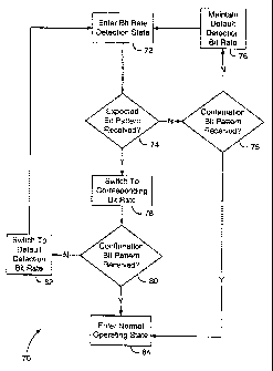
Fig. 7 is a flow diagram of a method of bit rate matching. The method 70
includes the steps performed at a receiving end of a data link to detect and
match a bit rate
used at a remote sending end of the data link. For the detection method 70,
which
includes confirmation of a detected bit rate, the sending er~d preferably
transmits a bit rate
detection bit pattern such as the data byte OxFF, followed by a confirmation
bit pattern.
Although referred to primarily as a receiving end or a receiver and a sending
end or a
sender, it should be appreciated that these receiving and sending
characterizations are
solely for the purposes of bit rate detection. In a preferred embodiment of
the invention, a
modem performs bit rate detection to detect a bit rate used by an external
processor or a
communications controller associated with the external processor. Data links
are typically
bi-directional, such that the receiver during bit rate detection, the modem in
this
embodiment, is the sender when data destined for the external processor is
received by
the modem.
At step 72, the receiver enters a bit rate detection state, in response to a
user
command, for example, or at some point during modem installation and
configuration.
Since bit rates of one nt" (n an integer) a receiver bit rate are detected as
described above,
the receiver is preferably set to a maximum supported bit rate at step 72 so
that bit rates at
or below the maximum bit rate can be detected.
The receiver then determines, at step 74, whether an expected bit pattern
has been received. The bit rate detection bit pattern and any of a plurality
of
predetermined bit patterns arising from start bit extension comprise expected
bit patterns.
Where none of the expected bit patterns is received, then the receiver
determines at step
75 whether the confirmation bit pattern has been received. Where the
confirmation bit
-13-
CA 02424213 2003-03-31
pattern has been received, a current bit rate is maintained, and the receiver
enters a
normal operating state at step 84 and uses the current bit rate for
communications over the
data link. Step 75 allows a sender to transmit the confirmation bit pattern
without first
sending the bit rate detection bit pattern, to effectively select a highest
supported bit rate
used for bit rate detection, for example. If neither are expected bit pattern
nor the
confirmation bit pattern is received, then a default bit rate used at the
receiver for bit rate
detection, preferably a maximum bit rate, is maintained at step 76, and
processing reverts
back to step 72 to await a data transmission from the sender.
When an expected bit pattern is detected, the receiver adjusts its bit rate
accordingly, at step 78. If OxFF was received, then the current detection bit
rate is
maintained. Otherwise, another bit rate is selected. The receiver then awaits
a
confirmation bit pattern at step 80. If the confirmation bit pattern is
correctly received, then
the receiver enters a normal operating state at step 84, and uses the adjusted
bit rate for
communications over the data link. Where the receiver does not receive the
confirmation
bit pattern within a predetermined period of time, then at step 82 it switches
to or maintains
a default bit rate used for bit rate detection, such as the maximum bit rate,
and the method
reverts back to step 72. Thus, bit rate adjustments take effect only when
confirmed.
Those skilled in the art will appreciate that the method 70 is intended for
illustrative purposes only. The present invention is in no way limited
thereto. For example,
in order to avoid an endless loop from step 75 or step 80 to step 72, such as
when a data
link is not operating properly, the method may proceed to step 84 or declare
an error after
some maximum number of negative determinations at step 74 or step 80.
Another modification to the methad 70 supports discrimination between bit
-14-
CA 02424213 2003-03-31
rates below one ninth the detection bit rate. For a bit rate equal to or below
one ninth the
detection bit rate, OxFF is received as 0x00. In a low bit rate discrimination
embodiment,
the receiver is configured to interpret 0x00 as an expected bit pattern at
step 74, and to
adjust to a low detection bit rate, such as one ninth a current detection bit
rate, at step 78
in response thereto. For bit rates below one ninth a current detection bit
rate, the start bit
is extended to a tenth bit sample at the receiver, and as such, could be
interpreted as a
framing error (i.e., an expected stop bit is not detected). 'therefore, the
transition to step
76 may be made responsive to detection of a framing error or an all-zeros
pattern at step
74. In this case, the sender may be configured to send an initial data byte
such as OxFF,
or any other data byte in this case, to the receiver to cause the framing
error or all-zeros
pattern and thereby trigger detection bit rate reduction at step 76.
Alternatively, step 74
may also be time-dependent, such that the bit rate is lowered at step 76 if
the receiver
does not receive an expected bit pattern within a predetermined time after
entering the bit
rate detection state. Thus, the sender sends OxFF after either the initial
data byte or the
predetermined time, followed by the confirmation bit pattern.
In one embodiment, the modem 16 (Fig.1 ) is a GPRS modem supporting bit
rates up to a maximum of 115.2kbps. Using the bit rate detection techniques
described
above, bit rates such as 115.2kbps, 57.6kbps (one half), ~8.4kbps (one third),
28.8kbps
(one quarter), and 19.2kbps (one sixth), for example, are detected when OxFF
OxFE, OxFC,
OxFB, and OxEO, respectively, are received in a bit rate detection state with
115.2kbps as
the detection bit rate. In a low bit rate discrimination embodiment, reduction
of the
detection bit rate to 14.4kbps (one eighth), allows detection of still lower
common bit rates
of 4800bps (one twenty-fourth the maximum bit rate), 2400bps (one forty-eighth
the
-15-
CA 02424213 2003-03-31
maximum bit rate), and 1800bps (one sixty-fourth the maximum bit rate), for
example. Still
lower bit rates are similarly detectable if the detection bit rate is further
reduced. As
described above, however, this magnitude of bit rate mismatch may be rare.
It will be appreciated that the above description relates to preferred
embodiments by way of example only. Many variations on the systems and methods
described above will be obvious to those knowledgeable in the field, and such
obvious
variations are within the scope of the invention as described and claimed,
whether or not
expressly described.
For example, although described primarily ire the context of a local data link
on an electronic device, the bit rate detection techniques described above may
also be
applied to other types of data links, including those between a modem and a
remote
communication device or system, or between other components associated with
the same
or different electronic devices.
It should also be appreciated that the invention is in no way limited to
implementation in conjunction with a wireless modem, or any other type of
modem. The bit
rate detection techniques described above may be applied to any asynchronous
serial data
link.
-16-