Note: Descriptions are shown in the official language in which they were submitted.
CA 02424855 2011-04-11
CASCADE LOW-PASS FILTER TO IMPROVE xDSL BAND
ATTENUATION FOR POTS SPUTTER
TECHNICAL FIELD OF THE INVENTION
[0002] The present invention relates generally to telecommunications, and in
particular
to low-pass filters for use in POTS splitters and xDSL modems.
BACKGROUND OF THE INVENTION
[0003] A variety of telecommunication systems utilize traditional telephone
company
local subscriber loops to carry high rate digital transmissions. Examples
include a variety
of digital subscriber loop (DSL) services, such as high-rate DSL (HDSL),
asymmetric DSL
(ADSL), very high-rate DSL (VDSL) and others. The varieties of DSL service
will be
referred to herein generally as xDSL.
[0004] The xDSL services share the same carrier with traditional analog
telephony,
commonly referred to as plain old telephone service (POTS). To share the same
carrier,
some soil of multiplexing is used. Typically, this involves frequency division
multiplexing
(FDM). POTS typically occupies the frequencies of between 300 and 3400 Hz
while the
xDSL service typically occupies some band of frequencies above the POTS
service.
[0005] To isolate the POTS service from the xDSL transceiver, a splitter, or
POTS
splitter, is used. These splitters generally have a low-pass filter to permit
passing of the
POTS service and a high-pass filter to permit passing of the xDSL service. To
provide
maximum possible transfer of power of a signal between a source and its load,
the POTS
splitter must have its impedance matched to the transmission line or carrier.
[0006] For the reasons stated above, and for other reasons stated below that
will
become apparent to those skilled in the art upon reading and understanding the
present
specification, there is a need in the art for alternative apparatus and
methods to facilitate
line impedance matching in a POTS splitter.
1
CA 02424855 2011-04-11
SUMMARY
[0007] The various embodiments utilize resistance in parallel with one or more
inductors in a series leg of a low-pass filter. This parallel resistance
facilitates changes to
the input and output resistance of the filter with little or no change in the
reactance of the
inductors. Furthermore, the reactance of the capacitors in the shunt legs of
the filter will be
substantially unaffected. This assists the designer in matching the impedance
of the filter
in the pass-band while still providing substantial impedance mismatching in
the stop-band
without substantially affecting the characteristics of the filter.
Facilitating impedance
matching in the pass-band and impedance mismatching in the stop-band is
accomplished
without the need for more complex active components. Various embodiments may
further
contain additional components that do not materially affect the basic and
novel properties
of the devices disclosed herein.
[0008] The various embodiments include sixth-order elliptic low-pass filters
and POTS
splatters including such filters of varying scope. The design of the sixth-
order filter
comprises two stages. A first stage includes a fourth-order filter, preferably
with a stop-
band frequency of approximately 48 kHz. A second stage includes a second-order
filter in
cascade with the fourth-order filter. For this filter, the stop-band frequency
is preferably
approximately 29 kHz. The inductance value of the second stage is relatively
small in
comparison to the inductance values of the first stage. In this manner,
improvements in
xDSL band attenuation are facilitated with little or no eroding of the voice
band
performance such as insertion loss, pass-band attenuation and return loss.
According to the invention, there is provided a low-pass filter, further
comprising:
an eighth capacitor in parallel with the first resistor;
a ninth capacitor in parallel with the second resistor;
a fourth resistor in parallel with the first capacitor; and
a fifth resistor in parallel with the second capacitor.
2
CA 02424855 2011-04-11
According to the invention, there is also provided a low-pass filter,
comprising:
a first differential mode inductor in series with a second differential mode
inductor, wherein the first differential mode inductor has an inductance value
of
approximately 21 mH and wherein the second differential mode inductor has an
inductance value of approximately 10 mH;
a third differential mode inductor in series with the second differential
mode inductor, wherein the third differential mode inductor has an inductance
value
of approximately 2.8 mH;
first and second resistors in parallel with the first differential mode
inductor, wherein the first and second resistors each have a resistance value
of
approximately 2.37 kQ;
first and second capacitors in parallel with the second differential mode
inductor, wherein the first and second capacitors each have a capacitance
value of
approximately 0.0022 pF;
third and fourth capacitors in parallel with the third differential mode
inductor, wherein the third and fourth capacitors each have a capacitance
value of
approximately 0.022 pF;
a first shunt leg interposed between the first and second differential mode
inductors and coupled across a first and second winding of the first
differential mode
inductor, wherein the first shunt leg comprises a fifth capacitor having a
capacitance
value of approximately 0.022 pF and a third resistor coupled in series with
the fifth
capacitor and having a resistance value of approximately 51.1 Q;
a second shunt leg interposed between the second and third differential
mode inductors and coupled across a first and second winding of the second
differential mode inductor, wherein the second shunt leg comprises a sixth
capacitor
having a capacitance value of approximately 0.036 pF; and
2a
CA 02424855 2011-04-11
a third shunt leg coupled across a first and second winding of the third
differential mode inductor, wherein the third shunt leg comprises a seventh
capacitor
having a capacitance value of approximately 0.01 pF;
wherein the third differential mode inductor is interposed between the
second shunt leg and the third shunt leg.
According to the invention, there is also provided a low-pass filter,
comprising:
a fourth-order first stage comprising:
a first differential mode inductor in series with a second differential
mode inductor;
first and second resistors in parallel with the first differential mode
inductor, wherein the first and second resistors each have approximately the
same
resistance value;
first and second capacitors in parallel with the second differential
mode inductor, wherein the first and second capacitors each have approximately
the
same capacitance value;
a first shunt leg interposed between the first and second differential
mode inductors and coupled across a first and second winding of the first
differential
mode inductor; and
a second shunt leg interposed between the second and third
differential mode inductors and coupled across a first and second winding of
the
second differential mode inductor;
a second-order second stage in cascade with the first stage, the second
stage comprising.
a third differential mode inductor having an inductance value of less
than half of an inductance value of the first differential mode inductor or an
inductance value of the second differential mode inductor;
2b
CA 02424855 2011-04-11
third and fourth capacitors in parallel with the third differential mode
inductor, wherein the third and fourth capacitors each have approximately the
same
capacitance value; and
a third shunt leg coupled across a first and second winding of the
third differential mode inductor;
wherein the third differential mode inductor is interposed between
the second shunt leg and the third shunt leg.
According to the invention, there is also provided a low-pass filter,
consisting essentially of:
a first differential mode inductor in series with a second differential mode
inductor and a third differential mode inductor;
a first resistor in parallel with a first winding of the first differential
mode
inductor,
a second resistor in parallel with a second winding of the first differential
made inductor;
a first capacitor in parallel with a first winding of the second differential
mode inductor;
a second capacitor in parallel with a second winding of the second
differential mode inductor;
a third capacitor in parallel with a first winding of the third differential
mode inductor;
a fourth capacitor in parallel with a second winding of the third differential
mode inductor;
a first shunt leg comprising a first end coupled between the first windings
of the first and second differential mode inductors and a second end coupled
between the second windings of the first and second differential mode
inductors;
a second shunt leg comprising a first end coupled between the first
windings of the second and third differential mode inductors and a second end
2c
CA 02424855 2011-04-11
coupled between the second windings of the second and third differential mode
inductors; and
a third shunt leg comprising a first end coupled to the first winding of the
third differential mode inductor and a second end coupled to the second
winding of
the third differential mode inductor;
wherein the third differential mode inductor is coupled between the
second and third shunt legs.
According to the invention, there is also provided a POTS splitter,
comprising:
a low-pass filter for coupling between an xDSL out port and a POTS port,
wherein the low-pass filter comprises:
first, second and third differential mode inductors in series between the
POTS port and the xDSL out port;
first and second resistors in parallel with the first differential mode
inductor;
first and second capacitors in parallel with the second differential mode
inductor;
third and fourth capacitors in parallel with the third differential mode
inductor;
a first shunt leg interposed between the first and second differential mode
inductors and coupled across the first and second differential mode inductors;
a second shunt leg interposed between the second and third differential
mode inductors and coupled across the second and third differential mode
inductors;
and
a third shunt leg coupled across the third differential mode inductor.
According to the invention, there is also provided a POTS splitter,
comprising.
a low-pass filter for coupling between an xDSL out port and a POTS port,
wherein the low-pass filter comprises:
2d
CA 02424855 2011-04-11
a first differential mode inductor having a first winding and a second
winding, wherein the first winding corresponds to a tip line and the second
winding
corresponds to a ring line;
a second differential mode inductor in series with the first differential
made inductor and having a first winding and a second winding, wherein the
first
winding corresponds to the tip line and the second winding corresponds to the
ring
line;
a third differential mode inductor in series with the first and second
differential mode inductors and having a first winding and a second winding,
wherein
the first winding corresponds to the tip line and the second winding
corresponds to
the ring line;
a first resistance in parallel with the first winding of the first
differential mode inductor;
a second resistance in parallel with the second winding of the first
differential mode inductor;
a first capacitance in parallel with the first winding of the second
differential mode inductor;
a second capacitance in parallel with the second winding of the
second differential mode inductor;
a third capacitance in parallel with the first winding of the third
differential mode inductor;
a fourth capacitance in parallel with the second winding of the third
differential mode inductor;
a fifth capacitance in series with a third resistance coupled between
the tip line and the ring line;
a sixth capacitance coupled between the tip line and the ring line;
and a seventh capacitance coupled between the tip line and the ring line;
wherein the fifth capacitance and the third resistance are interposed
between the first and second differential mode inductors;
2e
CA 02424855 2011-04-11
wherein the sixth capacitance is interposed between the second and
third differential mode inductors; and
wherein the third differential mode inductor in interposed between
the sixth and seventh capacitances.
According to the invention, there is also provided a remote-side xDSL
modern, comprising:
a low-pass filter for coupling between an xDSL out port and a POTS port,
wherein the low-pass filter consists essentially of:
a first differential mode inductor in series with a second differential
mode inductor and a third differential mode inductor;
a first resistor in parallel with a first winding of the first differential
mode inductor, wherein the first winding of the first differential mode
inductor
corresponds to a tip line of the xDSL out port;
a second resistor in parallel with a second winding of the first
differential mode inductor, wherein the second winding of the first
differential mode
inductor corresponds to a ring line of the xDSL out port;
a first capacitor in parallel with a first winding of the second
differential mode inductor, wherein the first winding of the second
differential mode
inductor corresponds to the tip line of the xDSL out port;
a second capacitor in parallel with a second winding of the second
differential mode inductor, wherein the second winding of the second
differential
mode inductor corresponds to the ring line of the xDSL out port;
a third capacitor in parallel with a first winding of the third differential
mode inductor, wherein the first winding of the third differential mode
inductor
corresponds to the tip line of the xDSL out port;
a fourth capacitor in parallel with a second winding of the third
differential mode inductor, wherein the second winding of the third
differential mode
inductor corresponds to the ring line of the xDSL out port;
2f
CA 02424855 2011-04-11
a first shunt leg comprising a first end coupled between the first
windings of the first and second differential mode inductors and a second end
coupled between the second windings of the first arid second differential mode
inductors;
a second shunt leg comprising a first end coupled between the first
windings of the second and third differential mode inductors and a second end
coupled between the second windings of the second and third differential mode
inductors; and
a third shunt leg comprising a first end coupled to the first winding of
the third differential mode inductor and a second end coupled to the second
winding
of the third differential mode inductor;
wherein the third differential mode inductor is coupled between the
second and third shunt legs.
2g
CA 02424855 2003-04-09
BRIEF DESCRIPTION OF THE DRAWINGS
[0009] Figure 1 is a block diagram of a communication network having a POTS
splitter in accordance with an embodiment of the invention.
[0010] Figure 2 is a block diagram of a POTS splitter showing additional
detail on the
connections between the various carriers in accordance with an embodiment of
the
invention.
[0011] Figure 3 is a graph depicting the pass-bands and stop-band generally
used for a
POTS splitter.
[0012] Figures 4A-4B are schematics of POTS splitters in accordance with
embodiments of the invention.
[0013] Figures 5A-5B are graphs of a frequency response for a POTS splitter in
accordance with one embodiment of the type depicted in Figure 413.
DETAILED DESCRIPTION
[0014] In the following detailed description of the present embodiments,
reference is
made to the accompanying drawings that form a part hereof, and in which is
shown by way
of illustration specific embodiments in which the invention may be practiced.
These
embodiments are described in sufficient detail to enable those skilled in the
art to practice
the invention, and it is to be understood that other embodiments may be
utilized and that
logical, electrical or mechanical changes may be made without departing from
the scope of
the present invention. The following detailed description is, therefore, not
to be taken in a
limiting sense, and the scope of the present invention is defined only by the
appended
claims and equivalents thereof.
[0015] Impedance matching is necessary in the design of POTS splitters to
provide the
maximum possible transfer of signal power between a source and its load.
Mismatched
impedance in the transmission line can cause signal reflection, echo return
and power loss.
The maximum transfer power of a signal, from a source to its load, occurs when
load
3
CA 02424855 2003-04-09
impedance is equal to the complex conjugate of the source impedance. In other
words, the
impedance of source and load have the same real part and opposite reactance.
[0016] However, the designer generally does not have the ability to change the
filter
input and output impedance by changing the values of impedance (L) and
capacitance (C)
when the coefficient of the filter is calculated. Changing the values of L and
C in the filter
will change the cutoff frequency and attenuation of frequency response of the
filter.
Modifications of the input and output impedance can be accomplished using
active
filtering, but such complexity can lead to higher failure rates of installed
splatters.
Moreover, the use of active circuits in the filter can interfere with lifeline
POTS support.
Such lifeline POTS service is generally required by telephony companies for
emergency
access of the telecommunications system.
[0017] For one embodiment, filter impedance is modified by adding parallel
resistors
with one or more inductors in the series leg of the filter. This changes input
and output
resistance of a filter without changing the reactance of the inductors in the
series leg if the
quality, Q, is greater than 10. If Q is less than 10, reactance of the
inductors will see little
change. Furthermore, the reactance of the capacitors in the shunt legs of the
filter will be
substantially unaffected. Therefore, it will generally not change the
characteristics of the
filter to add parallel resistors to the inductors.
[0018] The various embodiments help facilitate impedance matching in a POTS
splitter for the pass-band of the low-pass filter portion while facilitating
impedance
mismatching in the stop-band of the low-pass filter. Various embodiments
include one or
two pairs of resistors in parallel with differential mode inductors in a sixth-
order elliptic
low-pass filter. By transforming a parallel circuit into the equivalent series
resistor and
inductance circuit, several tens of ohms resistance can be added to the
splitter in the pass-
band to improve line impedance matching and several kilo-ohms resistance can
be added
to the splitter in the stop-band to accelerate the impedance mismatching. The
circuit sees
an effective filter resistance that is larger than what is actually present.
This allows fine
tuning of the insertion loss, return loss and voice band attenuation due to
the change of line
impedance matching. It also accelerates the impedance mismatching in the xDSL
band to
4
CA 02424855 2003-04-09
improve attenuation. In addition, the network's quality factor, Q, can be
decreased, gain
overshoot in the frequency response can be reduced and bandwidth can be
increased
through proper selection of the parallel resistance values.
[0019] Figure 1 is a block diagram of a communication network 100 having a
POTS
splitter 101 coupled between a customer loop, or local loop carrier, and a
central office
(CO) POTS transceiver and DSL transceiver, such as a DSL access multiplexer
(DSL.AM)
ADSL transceiver unit (ATU). The primary components of the POTS splitter 101
include
the CO POTS low-pass filter and the RC high-pass filter. Typically, the POTS
splitter 101
would contain only the capacitive portion of the high-pass filter, relying on
modern,
circuitry to provide the resistive portion. Additional circuitry may include
overvoltage and
surge protection, a loop present indicator and a signature resistance for a CO-
side
application. The POTS splitter 101 includes a low-pass filter in accordance
with an
embodiment of the invention.
[00201 Figure 2 is a block diagram of a POTS splitter 101 showing additional
detail on
the connections between the various carriers. The POTS splitter 101 of Figure
2 includes a
low-pass filter 205, in accordance with an embodiment of the invention, having
a tip line
from the CO (central office) or RT (remote terminal) coupled to a tip line of
the local loop
and a ring line from the CO or RT coupled to a ring line of the local loop.
The POTS
splitter 101 of Figure 2 further includes a tip line from the ATU coupled to
the tip line of
the local loop and a ring line from the ATU coupled to the ring line of the
local loop. For
POTS systems in North America, the tip and ring lines generally present a
characteristic
impedance of approximately 900 S) for incoming signals and approximately 600 f
or less
for the return signals. The ATU will typically present a characteristic
impedance of
approximately 100 91. A POTS splitter is utilized at each loop termination,
i.e., two per
loop. As POTS termination impedance values are generally different at each
point, the
low-pass filters of the POTS splitters should also be different for each
termination.
[0021] Figure 3 is a graph depicting the pass-bands and stop-band generally
used for a
POTS splitter 101. The low-pass filter has a pass-band of approximately 0-4
kHz while
the high-pass filter has a pass-band of approximately 32 kHz and above. The
stop-band for
9
CA 02424855 2003-04-09
the low-pass filter is generally anything above its pass-band, particularly 32
kHz or above,
while the stop-band for the high-pass filter is generally anything below its
pass-band,
particularly 4 kHz or below.
[0022] Figure 4A is a schematic of a POTS splitter 101A in accordance with an
embodiment of the invention. The POTS splitter IOTA of Figure 4A includes a
high-pass
filter including capacitors C10 and C11 coupled between the ring and tip
lines,
respectively, of an xDSL in port, e.g., the CO ATU or other DSL transceiver,
and an xDSL
out port, e.g., the local loop. As noted earlier, the high-pass filter can
further include
resistive components (not shown) in an associated modem circuit. The POTS
splitter
101A may further include a solid state voltage suppressor 115 or other over-
voltage
suppression circuitry coupled between the ring and tip lines of the xDSL out
port. The
POTS splitter 101A may include circuitry 120 coupled between the ring and tip
lines of a
POTS port, e.g., a CO POTS transceiver, for providing loop presence indication
and
signature resistance. For one embodiment, the circuitry 120 includes series-
connected
diode CR2, zener diode or regulator CR3 and resistor R10. Fuses Fl and F2 may
be
inserted in the tip and ring lines, respectively, for further surge
protection. For example,
FI and F2 may represent 1.5A fuses.
[0023] The POTS splitter 101A of Figure 4A further includes a low-pass filter
including series-connected differential mode inductors Ti, T2 and T3. For one
embodiment, inductors Ti, T2 and T3 have inductance values in the range of
approximately 2 mH to approximately 30 mH. For one example embodiment, the
inductor
Ti has an inductance value of approximately 18 mH, the inductor T2 has an
inductance
value of approximately 22 mH and the inductor T3 has an inductance value of
approximately 2.8 mH.
[0024] The low-pass filter is a sixth-order elliptic low-pass filter. Inductor
Ti is
further coupled to resistors RI and R2, which are coupled across the tip lines
and ring
lines, respectively. The resistors RI and R2 are in parallel with separate
windings of the
inductor Ti. Inductor T1 is further coupled to capacitors C l and C2, which
are coupled
6
CA 02424855 2003-04-09
across the tip lines and ring lines, respectively. The capacitors Cl and C2
are in parallel
with the resistors RI and R2, respectively.
[0025] Inductor T2 is coupled to resistors R3 and R4, which are coupled across
the tip
lines and ring lines, respectively. The resistors R3 and R4 are in parallel
with separate
windings of the inductor T2. Inductor T2 is further coupled to capacitors C3
and C4,
which are coupled across the tip lines and ring lines, respectively. The
capacitors C3 and
C4 are in parallel with the resistors R3 and R4, respectively.
[0026] Inductor T3 is coupled to capacitors C5 and C6, which are coupled
across the
tip lines and ring lines, respectively. The capacitors C5 and C6 are in
parallel with
separate windings of the inductor T3. The resistors R1, R2, R3 and R4 may be
used to fine
tune the filter resistance to improve impedance matching with line and load
termination.
[0027] For one embodiment, the parallel resistor RI and the parallel resistor
R2 have
substantially the same resistance. For a further embodiment, the parallel
resistor R3 and
the parallel resistor R4 have substantially the same resistance. For a still
further
embodiment, the parallel resistors RI and R2 each have a lower resistance
value than the
parallel resistors R3 and R4. For one embodiment, the parallel resistors R1
and R2 have
resistance values greater than approximately I kQ. For a further embodiment,
the parallel
resistors R1 and R2 further have resistance values less than approximately 5
M. For one
embodiment, the parallel resistors R3 and R4 have resistance values greater
than
approximately 5 kQ. For a further embodiment, the parallel resistors R3 and R4
further
have resistance values less than or equal to approximately 30 kS2. For a still
further
embodiment, the parallel resistors R3 and R4 effectively prohibit current
flow, e.g.,
through increasing values of resistance or elimination of the resistors
altogether. In one
example embodiment, parallel resistors RI and R2 may have resistance values of
approximately 3.01 kQ and the parallel resistors R3 and R4 may have resistance
values of
approximately 5.62 kn.
[0028] For one embodiment, the parallel capacitors Cl and C2 have
substantially the
same capacitance. For another embodiment, the parallel capacitors C3 and C4
have
substantially the same capacitance. For still another embodiment, the parallel
capacitors
7
CA 02424855 2003-04-09
C5 and C6 have substantially the same capacitance. For one embodiment, the
parallel
capacitors CI and C2 have capacitance values of approximately one order of
magnitude
less than the capacitance values of the parallel capacitors C3 and C4. For
another
embodiment, the parallel capacitors Cl and C2 are eliminated. For yet another
embodiment, the parallel capacitors C5 and C6 have capacitance values of
approximately
one order of magnitude more than the capacitance values of the parallel
capacitors C3 and
C4. For one example embodiment, the parallel capacitors C1 and C2 have
capacitance
values of approximately 200 pF, the parallel capacitors C3 and C4 have
capacitance values
of approximately 0.002 F and the parallel capacitors C5 and C6 have
capacitance values
of approximately 0.016 F.
[0029] Shunt legs may be inserted between the tip and ring lines of the low-
pass filter.
For one embodiment, shunt capacitor C7 may be interposed between the inductor
Ti and
the inductor T2 and coupled between the tip and ring lines, e.g.., between the
separate
windings of the inductors T1 and T2. A resistor R7 may be coupled between the
tip and
ring lines in series with the capacitor C7. For a further embodiment, shunt
capacitor C8
may be interposed between the inductor T2 and the inductor T3 and coupled
between the
tip and ring lines, e.g., between the separate windings of the inductors 72
and T3. A
resistor R8 may be coupled between the tip and ring lines in series with the
capacitor C8.
For a still further embodiment, shunt capacitor C9 may be interposed between
the inductor
T3 and the POTS port and coupled between the tip and ring lines, e.g., between
the
windings of the inductor T3. A resistor R9 may be coupled between the tip and
ring lines
in series with the capacitor C9.
[0030] For one embodiment, the resistors R7, R8 and R9 have resistance values
of
approximately 100 0 or less. For another embodiment, the shunt capacitors C7,
C8 and
C9 have capacitance values of approximately 0.05 gF or less. For one example
embodiment, the resistors R7, R8 and R9 each have resistance values of
approximately
100 S2 while shunt capacitor C7 has a capacitance value of approximately 0.010
F, shunt
capacitor C8 has a capacitance value of approximately 0.030 liF, and shunt
capacitor C9
has a capacitance value of approximately 0.022 F.
8
CA 02424855 2003-04-09
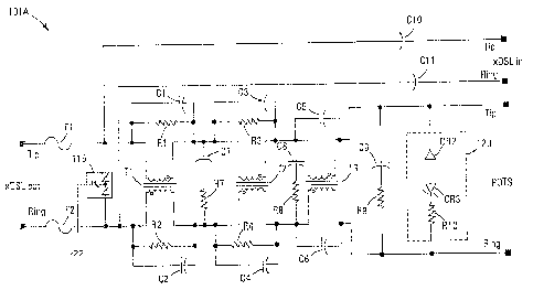
[0031] Figure 4B is a schematic of a POTS splitter 101B in accordance with
another
embodiment of the invention as an example of a splitter for a remote-side
modem. The
POTS splitter 1OIB is shown without the high-pass filter as both the resistive
and
capacitive components may reside as part of the modem. The POTS splitter 101B
may
include a solid state voltage suppressor 115 or other over-voltage suppression
circuitry
coupled between the ring and tip lines of the xDSL out port. A fuses Fl may be
inserted in
the tip or ring line for further surge protection- For example, FI may
represent a 1.5A
fuse. The signature resistance and loop presence indication may also be
eliminated from a
low-pass filter for a remote-side modem.
[0032] The POTS splitter 101B of Figure 4B further includes a low-pass filter
including series-connected differential mode inductors Ti, T2 and T3. For one
embodiment, the inductors Ti, T2 and T3 have inductance values in the range of
approximately 2 mH to approximately 25 mH. For one example embodiment, the
inductor
TI has an inductance value of approximately 21 mH, the inductor T2 has an
inductance
value of approximately 10 mH and the inductor T3 has an inductance value of
approximately 2.8 mH.
[0033] Inductor Ti is further coupled to resistors R1 and R2, which are
coupled across
the tip lines and ring lines, respectively. The resistors R1 and R2 are in
parallel with
separate windings of the inductor TI. Inductor T2 is coupled to capacitors C3
and C4,
which are coupled across the tip lines and ring lines, respectively.
[0034] Inductor T3 is coupled to capacitors C5 and C6, which are coupled
across the
tip lines and ring lines, respectively. The capacitors C5 and C6 are in
parallel with
separate windings of the inductor T3. The resistors RI and R2 may be used to
fine tune
the filter resistance to improve impedance matching with line and load
termination.
[0035] For one embodiment, the parallel resistor RI and the parallel resistor
R2 have
substantially the same resistance. For a further embodiment, the parallel
resistors RI and
R2 have resistance values greater than approximately 1 kf2. For a further
embodiment, the
parallel resistors RI and R2 further have resistance values less than
approximately 5 kn.
9
CA 02424855 2003-04-09
In one example embodiment, parallel resistors RI and R2 may have resistance
values of
approximately 2.37 M.
[0036] For one embodiment, the parallel capacitors C3 and C4 have
substantially the
same capacitance. For still another embodiment, the parallel capacitors C5 and
C6 have
substantially the same capacitance. For one embodiment, the parallel
capacitors C5 and
C6 have capacitance values of approximately one order of magnitude more than
the
capacitance values of the parallel capacitors C3 and C4. For one example
embodiment, the
parallel capacitors C3 and C4 have capacitance values of approximately 0.0022
F and the
parallel capacitors C5 and C6 have capacitance values of approximately 0.022
F.
[0037] Shunt legs may be inserted between the tip and ring lines of the low-
pass filter.
For one embodiment, shunt capacitor C7 may be interposed between the inductor
TI and
the inductor T2 and coupled between the tip and ring lines, e.g., between the
separate
windings of the inductors TI and T2. A resistor R7 may be coupled between the
tip and
ring lines in series with the capacitor C7. For a further embodiment, shunt
capacitor. C8
may be interposed between the inductor T2 and the inductor T3 and coupled
between the
tip and ring lines, e.g., between the separate windings of the inductors T2
and T3. For a
still further embodiment, shunt capacitor C9 may be interposed between the
inductor T3.
and the POTS port and coupled between the tip and ring lines, e.g., between
the windings
of the inductor T3.
[0038] For one embodiment, the resistor R7 has a resistance value of
approximately
100 S2 or less. For another embodiment, the shunt capacitors C7, C8 and C9
have
capacitance values of approximately 0.05 F or less. For one example
embodiment, the
resistor R7 has a resistance value of approximately 51.1 S2 while shunt
capacitor C7 has a
capacitance value of approximately 0.022 F, shunt capacitor C8 has a
capacitance value
of approximately 0.036 F, and shunt capacitor C9 has a capacitance value of
approximately 0.01 p.F.
[0039] The low-pass filter of Figure 4B is a sixth-order elliptic low-pass
filter. The
design of the sixth-order filter includes two stages. A first stage is a
fourth-order filter
between xDSL out and the second shunt leg (including the second shunt leg)_
For one
CA 02424855 2003-04-09
embodiment, this first stage has a stop-band frequency of approximately 48
kHz. The
stop-band frequency is determined by the capacitance of capacitors C3 and C4
and the
inductance of inductor T2. The filter frequency response of such an embodiment
exhibits a
notch at approximately 48 kHz as shown in Figure 5, At and above 48 kHz for
this fourth-
order filter, the attenuation may exceed 65dB. Generally, losses erode the
pass-band
performance more rapidly than the stop-band performance if the stop-band
frequency is
moved closer to 30 kHz by changing the values of C3, C4 and T2. For one
embodiment,
the attenuation at 32 kHz to 300 kHz is at least 65dB. A second stage includes
a second-
order filter in cascade with the fourth-order filter. For this filter, the
stop-band frequency
is approximately 29 kHz and is determined by the capacitance of capacitors C5
and C6 and
the inductance of inductor T3. The filter frequency response of Figure 5
exhibits a notch at
approximately 29 kHz corresponding to this second stage. Since the inductance
of T3 is
relatively small in comparison to the inductance of TI and T2, this greatly
improves the
xDSL band attenuation with little or no eroding of the voice band performance
such as
insertion loss, pass-band attenuation and return loss. For one embodiment, the
inductance
value of the inductor T3 is less than half of the inductance value of the
inductor Ti or the
inductor T2. For a further embodiment, the inductance value of the inductor T3
is less
than approximately 30% of the inductance value of the inductor T1 or the
inductor T2.
[0040] Mismatched impedance in the transmission line causes signal reflection,
echo
return and power loss. The maximum transfer of power of a signal from a source
to its
load occurs when load impedance is equal to the complex conjugate of the
source
impedance. In other words, the impedance of the source and load should have
the same
real part and opposite reactance.
[0041] For North American telephony systems, the POTS splitter generally needs
to
pass frequencies up to 3.4 kHz with less than 0.75dB for long loop and 1.00dB
for short
loop insertion loss at I kHz and to attenuate at least 65dB at a frequency
range of 32 kHz
to 300 kHz and 55dB at a frequency range of 300 kHz to 1104 kHz according to
the ANSI
T1.413 standard. Such standards also require voice band attenuation at 0.2 to
3.4 kHz of
+1.5dB to -1.5dB for short loop and of +0.5dB to -1.5dB for long loop. Such
standards
11
CA 02424855 2003-04-09
also require voice band attenuation at 3.4 to 4 kHz of +2.0dB to -2.0dB for
short loop and
of +1.0dB to -1.5dB for long loop. For RT-side applications, attenuation
should be greater
than 6dB for echo return loss (ERL), and greater than 5dB for singing return
loss low
(SRL-L) and 3dB for singing return loss high (SRL-H). For CO-side
applications,
attenuation should be greater than 8dB for ERL, and greater than 5dB for SRL-L
and 5dB
for SRL-H.
CONCLUSION
[0042] Impedance matching is necessary in the design of POTS splitters to
provide the
maximum possible transfer of signal power between a source and its load.
Mismatched
impedance in the transmission line can cause signal reflection, echo return
and power loss.
The maximum transfer power of a signal, from a source to its load, occurs when
load
impedance is equal to the complex conjugate of the source impedance. In other
words, the
impedance of source and load have the same real part and opposite reactance.
[0043] The various embodiments utilize resistance in parallel with the series
leg of the
low-pass filter. This parallel resistance facilitates changes to the input and
output
resistance of the filter with little or no change in the reactance of the
inductors.
Furthermore, the reactance of the capacitors in the shunt legs of the filter
will be
substantially unaffected. This assists the designer in matching the impedance
of the filter
in the pass-band while still providing substantial impedance mismatching in
the stop-band
without substantially affecting the characteristics of the filter.
Facilitating impedance
matching in the pass-band and impedance mismatching in the stop-band is
accomplished
without the need for more complex active components. Various embodiments may
further
contain additional components that do not materially affect the basic and
novel properties
of the devices disclosed herein.
[0044] The various embodiments include sixth-order elliptic low-pass filters
and POTS
splitters including such filters of varying scope. The design of the sixth-
order filter
comprises two stages. A first stage includes a fourth-order filter, preferably
with a stop-
band frequency of approximately 48 kHz. A second stage includes a second-order
low-
12
CA 02424855 2003-04-09
pass filter in cascade with the fourth-order filter. For this filter, the stop-
band frequency is
preferably approximately 29 kHz. The inductance value of the second stage is
relatively
small in comparison to the inductance values of the first stage. In this
manner,
improvements in xDSL band attenuation are facilitated with little or no
eroding of the
voice band performance such as insertion loss, pass-band attenuation and
return loss.
[0045] Although specific embodiments have been illustrated and described
herein, it
will be appreciated by those of ordinary skill in the art that any arrangement
that is
calculated to achieve the same purpose may be substituted for the specific
embodiments
shown. Many adaptations of the invention will be apparent to those of ordinary
skill in the
art. Accordingly, this application is intended to cover any such adaptations
or variations of
the invention. It is manifestly intended that this invention be limited only
by the following
claims and equivalents thereof.
13