Note: Descriptions are shown in the official language in which they were submitted.
CA 02424945 2003-04-04
WO 02/29465 PCT/USO1/29018
Transparent Substrate and Hinged Optical Assembly
Cross Reference to Related Applications
L 0 0 017 This application claims the benefits of U.S. Provisional Application
No.
60/239,058, filed October 5, 2000.
Field of the Invention
0 0 0 2 ~ This invention relates, in general, to fabrication of optical
devices and,
more particularly, to interconnecting optical devices and optical fibers.
Background of the Invention
L 0 0 0 3 ~ The coupling of an optical device or array of optical devices, an
optical
fiber or array of optical fibers, and an interconnecting substrate can be a
difficult task. Usually
the coupling is done manually or semi manually and can incur several problems
such as being
complex, inefficient, and not suitable for high volume manufacturing.
L 0 0 04 ] In order to reduce electrical parasitics, short electronic
interconnects are
needed between semiconductor photonic devices such as lasers and photodiodes
and electronic
interface circuitry. This electronic circuitry may include photonic signal
drivers and photonic
signal receivers. The need for decreased distance between photonic devices and
electrical
interface circuitry increases as the signaling data rate increases. Photonic
components are often
placed on simple carrier substrates to verify operation, to do burn-in, or
simply to facilitate
handling of that device. This photonic device and earner substrate are then
placed on another
substrate and additional packaging is completed. This packaging adds
additional electrical
interfaces, such as wire bonds and long non-controlled impedance wires,
decreasing the electrical
performance of the photonic device.
L 0 0 0 5 ~ In order to reduce optical losses and parasitics, efficient
coupling of
optical signals is needed. As optical signals tend to diverge from their
original transmission axis,
coupling devices or waveguides must be proximate optical transmitting and
receiving devices.
Signal loss increases with increased distances from an optical port to an
optical connector, unless
CA 02424945 2003-04-04
WO 02/29465 PCT/USO1/29018
light is adequately directed through a coupling device. One example of a setup
with limitations
because of increased distance between the optical device and optical fiber is
an electro-optic TO
can with an optical port. After placing the optical component in a can and
making electrical wire
bonds, further packaging must be done in the alignment with a fiber optic
cable. The distance
between the optical device and the fiber is often relatively large, minimizing
or eliminating the
possibility of multiple optical devices on the same semiconductor substrate.
With increased
distances between a waveguide and multiple optical devices disposed on the
same
semiconductor, optical cross tally can reduce signal integrity.
L 0 0 0 6 I Some prior art devices have reduced the length of electrical
and/or optical
interconnects by placing multiple components on a common, flexible substrate.
Other prior art
references teach of the use of Tensing systems to guide light appropriately,
thus allowing multiple
optical devices on the same semiconductor while minimizing optical losses.
Yet, Tensing may
require multiple optical couplings which can lead to signal loss. In addition,
multiple
waveguides require additional steps in aligning optical signals with an
external optical
waveguides and connectors, thus increasing manufacturing costs and decreasing
yield.
L 0 0 0 7 a Commonly used vertical cavity surface emitting laser (VCSEL)
structures
and photodiode structures have both electrical contacts and optical ports on
the same surface of
the semiconductor, creating packaging problems when trying to optimize the
performance of
each of these interfaces. These packaging problems are exacerbated when the
optical
components have arrays of optical devices. A novel packaging technique is
described below
under illustrated embodiments of the invention that combines complex
electrical and optical
trace patterns, and simplifies packaging by using a common transparent
substrate. This
transparent photonic circuit board could support arrays of photonic chips and
electrical interface
circuitry while reducing electrical losses, optical losses, and manufacturing
costs.
Summary of the Invention
L 0 0 0 8 ~ A method and apparatus are provided for providing an electro-optic
signal
processing device. The method includes the steps of providing an optically
transparent substrate
having first and second planar elements with an abutting common edge, the
planar elements
lying at differing angles with respect to each other about the common edge and
a plurality of
aligrsnent apertures formed in the substrate. A plurality of optical devices
of an optical array are
-2-
CA 02424945 2003-04-04
WO 02/29465 PCT/USO1/29018
disposed on the first planar element of the substrate, with transmission paths
of the optical
devices passing directly through the substrate. A signal processor is also
disposed on the first
planar element of the substrate. An optical fiber holder comprising a
plurality of respective
optical fibers and guide pin apertures disposed on a first surface of the
optical fiber holder is
aligned to the optical array using the guide pins and guide pin apertures.
Optical signals of the
optical devices of the optical array are coupled to respective optical fibers
of the aligned optical
fiber holder. A printed circuit board having a first surface is attached to a
mating surface of the
substrate's second planar element.
Brief Description of the Drawings
[ 0 0 0 9 ] FIG. 1 illustrates a perspective view of an electro-optic
communications
device in accordance with an illustrated embodiment of the invention, in a
context of use;
[ 0 010 ] FIG. 2 illustrates a bottom view of an optically transparent
substrate with
corresponding features and components on the substrate.
[ 0 011 ] FIG. 3 illustrates a side view of an optically transparent substrate
with
corresponding features and components on the substrate.
[ 0 012 ] FIG. 4 illustrates a perspective view of an optically transparent
substrate with
electrical traces traversing over a hinge on the substrate.
[ 0 013 ] FIG. 5 illustrates an enlarged perspective view of a removed portion
of the
substrate.
[ 0 014 ] FIG. 6 illustrates a top view of an electro-optic communication
system.
[0025] FIG. 7a illustrates a perspective view of a bent substrate with
corresponding components, features, and traces on the substrate.
[ 0 016 ] FIG. 7b illustrates a perspective view of a bent substrate with the
hinge in
a different location.
[ 0 017 ] FIG. 8a is a broken perspective view of a structural material
creating a
flexible interconnect region, in an alternate embodiment of the invention.
[ 0 018 ] FIG. 8b is a side view of a structural material creating a flexible
interconnect region, in an alternate embodiment of the invention.
-3-
CA 02424945 2003-04-04
WO 02/29465 PCT/USO1/29018
Detailed Description of a Preferred Embodiment of the Invention
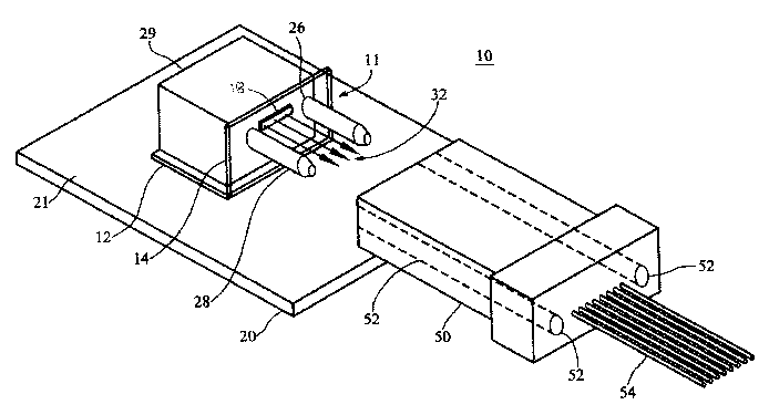
0 019 J FIG. 1 illustrates an electro-optic communications assembly 10 in a
context of
use, according to a preferred embodiment of the invention. Included in the
communications
assembly 10 may be a printed circuit board 20, optically transparent,
relatively rigid substrate 11
with a right angle bend, and an alignment mechanism 50 for holding optical
fibers 54 in
alignment with an active optical device 18. The printed circuit board 20 may
be any suitable
material such as FR4, ceramic interconnect, or the like. The printed circuit
board 20 may have a
plurality of electrical and optical devices for signal processing, as well as
electrical traces and
electrical pads (not shown in the figures). The optically transparent
substrate 11 may comprise
glass or a glass-like structure having desirable optical and structural
properties. The optically
transparent substrate 11 may be divided into an upright portion and a
horizontal portion. A
second surface 86 of the horizontal portion of the substrate 11 may be
attached to a first surface
of the printed circuit board 20 as shown in FIG. 1. A method for attaching may
include use of a
conductive adhesive or similar material.
0 0 2 0 7 FIG 2 illustrates a bottom view of a planarized optically
transparent substrate
11. The substrate 11 may include the active optical device 18, a signal
processor 16, electrical
traces 22, and electrical pads 24. It will be understood that the active
optical device 18 can be
any suitable photonic device or array of photonic devices including photo-
transmitters, photo-
receivers, or a combination thereof. A photo-transmitter can be any suitable
device such as a
vertical cavity surface emitting laser (VCSEL), light emitting diode (LED),,
or the like.
Furthermore, any suitable photo-receiving device can be used, such as a
photodiode, i.e., P-I-N
diode, PN diode, or the like. Thus, the active optical device 18 can be a
broad range of
photoactive devices with transmitting and receiving capabilities. Each optical
array may have a
number of optical ports 30 for coupling optical signals to a respective
photoactive device. The
optical ports 30 define the optically active surfaces of the optical device
18. The optical ports 30
provide an optical transmission path to photonics transmitters, receivers, or
a combination of
transmitters and receivers. The transmission paths 32 and 34 of the optical
device 18 may pass
directly through the substrate 11 to which the device 18 is attached, as shown
in FIG. 3. In the
view shown in FIG. 2, the transmission paths could be normal to the substrate
11 (i.e.,
transmitting out of the page).
-4-
CA 02424945 2003-04-04
WO 02/29465 PCT/USO1/29018
[ 0 0 21 J The substrate 11 may also comprise a signal processor 16. The
signal
processor 16 may be an amplifier mechanically attached to the substrate 11 by
a conductive
adhesive, solder bumps, or similar bonding technique. The signal processor 16
may be
electrically connected to the active optical device 18 by studlsolder bumps
with corresponding
electrical traces 22 that may traverse the length of the substrate 11.
Electrical traces 22 may be
defined on the substrate 11 by conventional photolithographic etching
processing, or a by any
similar process. The substrate 11 may also have electrical traces 22 and
electrical pads 24 for
electrically interconnecting components that are a combination of those
attached and those not
attached to the substrate 11. For example, wire bonds 60, (shown in FIG. 3),
may be disposed
between electrical pads 24 on the substrate 11 and nearby opto-electric
components, or to the
printed circuit board 20.
[ 0 0 2 2 J Alignment apertures 26 (FIG. 2) may also be provided on the
substrate 11. To
properly align the optical ports 30 of the optical array 18 to the optical
fibers 54 of the f ber
holding alignment mechanism 50, alignment apertures 26 are formed in the
substrate 11. The
apertures 26 passing through the substrate 11 may be disposed on opposing
sides of the optical
array 18, precisely positioned relative to the optical array 18 proximate a
first edge 80 of the
substrate 11. Alignment apertures 26 may be formed using conventional
techniques such as laser
ablation, chemical etching, plasma etching, or a similar process. Alignment
pins 28 may be
inserted concurrently through the apertures 26 formed in the substrate 11 and
into apertures 52
formed on a first surface 56 of the fiber holding alignment mechanism S0,
thereby aligning the
optically transparent substrate 11 and optical array 18 with the fiber holding
alignment
mechanism 50 and its respective optical fibers 54. In a preferred embodiment
of the invention,
the fiber holding alignment mechanism 50 could be a standard MT connector
manufactured by
US Conec or Nippon Telephone & Telegraph (US Conec Part number MTF-12MM7).
[ 0 0 2 3 ~ The alignment pins 28 aligning the optical array 18 to the fiber
holding
alignment mechanism 50 may be held in place by an alignment pin holder 29. The
pin holder 29
may be located proximate the first surface 84 of the substrate 11, opposite
the fiber holding
alignment mechanism 50. The pin holder 29 (shown in FIG. 1) may be attached to
the electrical.
IC 16. The electrical IC 16 is shown, in FIG. 8b, attached to the substrate 11
by a conductive
adhesive 62, or similar material. The guide pins 28 may be attached to the pin
holder 29 by an
-5-
CA 02424945 2003-04-04
WO 02/29465 PCT/USO1/29018
adhesive, or the pins 28 and holder 29 could be formed by a conventional
insert molding or
compression fit process.
0 0 2 4 ] FIG. 3 illustrates a side view in an embodiment of the invention.
Here the
electrical IC 16 is shown electrically connected to the substrate 11 by means
of wire bonds 60.
The wire bonds 60 may be attached to electrical pads 24, which may be attached
to electrical
traces 22, which may be attached to the substrate 11. It is understood that
the electrical IC can
be electrically connected to the substrate 11 by additional means such as
solder or stud bumps.
The optical IC 18 can also be electrically connected to the substrate 11 by
means of wire bonds,
stud bumps, solder bumps, or any other similar electrical attachment method.
0 0 2 5 ] Also shown in FIG. 3 is the optical transmission axis 32 and 34. The
optical device 18 could be a transmitting device, and light would propagate
from the device 18
and travel through the substrate 11 in the direction 32 shown. The optical
device 18 could be a
receiving device, and light coming in the direction of the arrow 34 would pass
through the
substrate 11 and strike the receiving device 18. In either case, optical
energy 32 and 34 would
pass directly through the optically transparent substrate 11. In an embodiment
of the invention
shown in FIG. 3 using an example of a laser for the optical array 18, light
must propagate 32
through the substrate 11 and away from or at least parallel to the planar
surface 21 to which the
substrate 11 is attached. Otherwise, if the substrate 11 did not have the
right-angle bend as
shown in FIG. 1, then light would strike the surface the top surface 21 of the
PCB 20, the surface
to which the substrate 11 is mounted to, and not enter a waveguide 50. Yet, if
the portion of the
substrate 11 having optical energy paths 32 and 34 was not in direct contact
with the PCB 20, a
waveguide could then be placed proximate the opposing surface 86 of the
substrate 11.
0 0 2 6 ] As shown in FIG.'s 1, 7a, and 7b, the substrate 11 may have a 90
degree
bend to allow optical signals to travel parallel to the PCB 20. As illustrated
in FIG.'s 4, 5, 7a,
and 7b the 90 degree bend in the substrate 11 may be formed by breaking the
substrate along a
groove 46 and rotating a portion of the substrate 11 about the groove 46.
After breaking, the
substrate 11 may then become a two-member body, having relatively rigid planar
elements 12
and 14. The groove 46, shown in the greatly enlarged underside cut-a-way view
of FIG. 5, may
be formed on the second surface 86 of the substrate 11, along the width 72 of
the substrate 1 l,
and at any location along the length 74 of the substrate 11. The groove 46
could be formed using
a conventional laser ablation, laser scribing, or mechanical scribing process.
The groove 46 may
-6-
CA 02424945 2003-04-04
WO 02/29465 PCT/USO1/29018
traverse the width 72 while not extending through the thickness 76 of the
substrate 1 l, as
illustrated in FIG. 5 (i.e., about 90% through the thickness). If the groove
46 is formed
completely through the thickness 76 of the substrate, the electrical traces 22
could be damaged or
separated. The broken substrate 11 with first and second planar elements 12
and 14 may have an
abutting common edge 70, as shown in FIG. 4. Upon forming the groove 46
partially through
the substrate 1 l, the grooved substrate 11 could be placed in a mechanical
fixture that could
break the substrate 1.1 by rotating a planar element 12 or 14 about the groove
46 with respect to
the other planar element.
t 0 0 2 7 7 The first and second planar elements 12, 14 may be rotated to any
position
with respect to the common edge 70. Once rotated, the first and second planar
elements 12, 14
may lie at differing angles with respect to each other about the common edge
70 (e.g., the planar
elements may form an angle of 90 degrees on one side and 270 degrees on the
other side).
[ 0 0 2 8 ] Conductive traces 22 may traverse the substrate 11 (i.e., connect
the two
halves 12, 14 of the substrate 11) and may structurally and electrically
interconnect the two
planar elements. The conductive traces 22 traversing the two planar elements
may form a hinge
42 extending the width 72 of the substrate 11 (the hinge 42 being located
along the common
edge 70). The second planar element 14 may be rotated along the hinge 42 to
any desired angle
88. In a preferred embodiment of the present invention, the second planar
element 14 may be
rotated ninety degrees, forming a ninety-degree angle with the substrate's
first planar element 12.
Rotating of the substrate to a desired angle 88 could complete the process of
breaking the
substrate 11 into two sections 12 and 14. That is, the planar substrate 11
could be broken and
rotated to a desired angle 88 by necessarily rotating the second planar
element 14 of the substrate
11 about the hinge 42, thus eliminating the specific manufacturing process of
breaking the
substrate 11. Rotating the second planar element 14 of the substrate 11 allows
the transmission
axis 32 and 34 of the optical array I 8 to be aligned parallel to the first
planar element 12 of the
substrate 11, further promoting planarity and thus manufacturability.
[ 0 0 2 9 ] FIG. 6 is a top view illustrating the mating of the second surface
86 of the
second planar element 14 of the substrate 11 with the first surface 56 of the
optical fiber holder
50. The alignment pins 28 may be inserted through the alignment apertures 52
of the fiber
holder 50. As shown in FIG. 1 and 6, the alignment pin holder 29 may restrict
rotation 88 of the
second planar element 14 about the hinge 42. The pin holder 29 and the first
surface 84 of the
_7_
CA 02424945 2003-04-04
WO 02/29465 PCT/USO1/29018
second planar element 14 may then be mechanically attached by an adhesive 62
or similar
material, once the desired angle of rotation 88 is achieved. The alignment pin
holder 29 may
also contain a removed section 31 located proximate the optical array 18. The
removed section
31 may prevent the pin holder 29 from coming in contact with and hence
exerting a force on the
optical array 18 and possibly causing damage. Thus, the section 33 of the pin
holder 29 without
a removed section 31 may then come in contact with the first surface 84 of the
second planar
element 14 of the substrate 11. The first surface 56 of the optical fiber
holder 50 may be
coincident with the second surface 86 of the second planar element 14 of the
substrate 11, as
shown in FIG. 6. Optical signals 32 and 34 passing directly through the second
planar element
14 of the substrate 11 would form an optical interface of light transmission.
Alternative Embodiments of the Invention
L 0 0 3 0 ] As previously stated, the substrate's break region or hinge 42
could be
located at any location along the length 74 of the substrate. In a preferred
embodiment of the
invention the groove 46 on the substrate 11 would be located between the
optical array 18 and
the electrical IC 16 on the second surface 86 of the substrate 11. In an
additional embodiment of
the invention shown in FIG 7b; the groove 46 and corresponding hinge 42 could
be located on
the substrate 11 between a second edge 82 and the electrical IC 16.
0 0 31 ] In another embodiment of the invention, the bending of the substrate
11
could be performed by using a heated wire bending process, thus eliminating
the laser ablation
process. The substrate 11 could be placed in a mechanical fixture that would
heat a portion of
the substrate 11 using a thin, hot wire. The temperature of the substrate 11
would rise
appropriately to facilitate the bending of the substrate 11. The substrate 11
would not have a
break region, but would have a hinge 42 as stated before.
0 0 3 2 ] FIG. 8a and FIG. 8b show a thin, structural material 44 that could
be
disposed on the hinge 42 of the substrate 11, on the first surface 84, in an
alternate embodiment
of the invention. This material could be placed on the hinge Whether a heated
wire or laser
ablation process is used to bend the substrate 11. The material could comprise
a flexible
insulative material such as a polyimide. Common trade names for polyimide are
"KAPTON"
and "UPLEX." The material 44 could form a layer over the electrical traces 22,
58 on the hinge
42.
_g_
CA 02424945 2003-04-04
WO 02/29465 PCT/USO1/29018
[ 0 0 3 3 ] Additional traces 58 could be placed on the substrate as shown in
FIG.'S 4,
7a, 7b, and 8a. The traces could be formed using conventional photolithography
etching
techniques, or a similar process. The traces could provide mechanical strength
in supporting the
second planar element 14 of the substrate 14 in the desired angular position
88.
[ 0 0 3 4 ] An additional mechanical strength (not shown) layer could be
deposited
over the metal traces, bonding to both the first layer of polyimide 44 and the
traces 22 and 58,
thus creating a flex interconnect region. Additional metal traces (not shown)
could traverse over
this flex region to provide additional mechanical interconnection or to
provide a ground plane.
The flexible, structural material 44 could be applied before the substrate 11
is broken and rotated
by a liquid deposition process. The thin layer 44 could be formed by using a
spinning and
screen-printing process.
[ 0 0 3 5 ] While a specific embodiment of the invention has been shown and
described, further modifications and improvements will occur to those skilled
in the art. This
invention, therefore, is not limited to the particular forms shown, and the
appended claims cover
all modifications that do not depart from the spirit and scope of this
invention.
_9_