Note: Descriptions are shown in the official language in which they were submitted.
CA 02425347 2003-04-14
CONTROL APPARATUS AND CONTROL METHOD
BACKGROUND OF THE INVENTION
1. Field of the Invention
The present invention relates to a control apparatus
and control method using direct memory access.
2. Description of Related Art
Drive mechanisms used in the latest electronic devices
require extremely fast, accurate operation. One control
method known to be able to satisfy these requirements uses
direct memory access (DMA). DMA enables data to be sent by a
dedicated hardware circuit directly from memory to the drive
mechanism controller instead of passing first through the
CPU. Because the drive mechanism can be controlled without
calling the CPU with this method, DMA is also compatible
with high speed operation of the drive mechanism.
Japanese Patent Laid-Open Publication (kokai) 2001-
327191, for example, teaches a control apparatus that
applies DMA to controlling a printer drive mechanism. This
control apparatus has a timing data table storing timing
data defining the timing at which control changes, and a
control data table storing control data used each time
control changes. After a CPU drive start request is asserted
a first DMA channel sends timing data from the timing data
table to the timer, and each time the timer times out an
activate signal is sent to a second DMA channel. Each time
this second DMA channel receives an activate signal, it
sequentially supplies control data stored to the control
data table to the drive mechanism control unit. Once the CPU
issues the drive start request, this configuration thus
enables controlling the drive mechanism according to
predefined timing data and control data without involving
the CPU.
1
CA 02425347 2003-04-14
Furthermore, the second DMA channel has plural DMA
channels corresponding to each of plural control data
types. When DMA transfer of the first control data is
completed by activation of the first DMA channel, the next
DMA channel is activated to pass the second control data,
and so forth. DMA control can thus be used to operate a
drive mechanism based on plural cantrol data types.
More specifically, the above-cited control apparatus is
configured to link operation of plural DMA channels in a
control chain, thereby enabling controlling a drive
mechanism using plural types of control data without
involving the CPU.
[Problem to be solved
As described above, when an activate signal is applied
to the second DMA channel in the conventicinal control
apparatus described above, the plural DMA channels in the
second DMA channels are automatically activated in sequence.
This makes it difficult to achieve complicated control
processes, such as supplying control data with different
timing to plural controlled objects, because the activation
timing of these plural DMA channels cannot be separately
controlled.
SU1~RY' OF THE INVENTION
The present invention is directed to solving the above
problem, and an object of this invention is to provide a
control apparatus and control method enabling more complex
control applications using direct memory access.
To achieve this object a control apparatus according to
the present invention sends control data appropriate for a
specific control unit to each of multiple control units each
running a process based on one or multiple types of control
data. The control apparatus has a first DMA processing unit
that is activated each time a specific first activation
signal is received, reads control data of a type compatible
with a specific first control unit from memory, and
transfers the control data to the first control unit, and a
2
CA 02425347 2003-04-14
second DMA processing unit that is activated each time a
specific second activation signal is received, reads data
of a type compatible with a specific second control unit
from memory, and transfers the control data to the second
control unit. The first DMA processing unit has a DMA
activation means for executing a process sending the second
activation signal to the second DMA processing unit.
The first DMA processing unit for transferring control
data to the first control unit can therefore start the
second DMA. processing unit to transfer control data to the
second control unit. Control data can thus be synchronously
transferred to the first and second control units.
This control apparatus preferably also has first and
second control data tables from which control data is read
by the first and second DMA processing units, and control
data setting means for writing control data to the first and
second control data tables. Thus comprised, control data
preset to the first and second control data tables can be
transferred respectively to the first and second control
units. More specifically, the first and second control units
can be operated according to the preset control data.
Further preferably, the control apparatus also has a
first clock means for outputting a specific time-up signal
when a time specified by received timing data passes after
the timing data is received, and a first DMA timing means
that is activated each time a specific activation signal is
received, reads timing data specifying a change-operation
timing for the first control unit from memory, and sends the
timing data to the first clock means. The time-up signal
output by the first clock means is sent to the first DMA
processing unit as the first activation signal, and the
first DMA processing unit activates the first DMA timing
means when it completes the data transfer operation.
Sending the first activation signal to the first DMA
processing unit when the time indicated by the timing data
passes after the activation signal is sent to the first DMA
timing means causes the first DMA timing means to start
again, and when the time specified by the timing data next
3
CA 02425347 2003-04-14
passes, the first DMA processing unit is activated. When
the first DMA processing unit activates, that is, when the
control data is transferred to the first control unit, can
thus be specified using the timing data.
Yet further preferably, the control apparatus also has
a timing data table from which the first DMA timing means
reads timing data, and a timing data setting means for
setting timing data in the timing data table.
Thus comprised the transfer timing for sending the
control data to the first DMA processing unit can be
controlled based on the timing data preset in the timing
data table.
Yet further preferably, a control apparatus according
to the present invention has a second clock means for
outputting a specific time-up signal when a time specified
by received timing data passes after the timing data is
received. The DMA activation means has a second DMA timing
means that reads and sends timing data from memory to the
second clock means each time the first activation signal is
received. The time-up signal output by the second clock
means is sent as the second activation signal to the second
DMA processing unit. It is therefore possible to set the
activation timing of the second DMA processing unit based on
the timing data sent by the second DMA timing means.
Yet further preferably, the first DMA processing unit
has one or multiple DMA channels disposed according to each
type of control data compatible with the first control unit
for reading from memory and transferring to the first
control unit control data of the compatible type one data
unit at a time.
Yet further preferably in this case the second DMA
processing unit has one or multiple DMA channels disposed
according to each type of control data compatible with the
second control unit for reading from memory and transferring
to the second control unit control data of the compatible
type one data unit at a time. The first DMA processing unit
has a DMA-operation-controlling DMA channel for reading from
memory and transferring to a control register of at least
4
CA 02425347 2003-04-14
one DMA channel disposed to the second DMA processing unit
operation control data specifying the data transfer
operation of that one DMA channel. When there are plural
types of control data used by the second control unit, it is
therefore possible to send data of each type separately to
the second control unit. In addition, the data transfer
operation of at least one DMA channel in the second DMA
processing unit can be specified by the DMA-operation-
controlling DMA channel of the first DMA processing unit. In
other words, the first DMA processing unit can change the
operation of the second DMA processing unit.
Yet further preferably, one DMA channel of the first
DMA processing unit is activated by the first activation
signal, and thereafter the other DMA channels are
sequentially activated.
Yet further preferably, the operation control data
specifies any of the following: DMA channel data transfer
source, data transfer destination, data transfer count, or
linked DMA channel indicating a DMA channel to be activated
next.
Yet further preferably, the second DMA processing unit
comprises a specific first DMA channel and a plurality of
second DMA channels that can be activated by the first DMA
channel. The DMA-operation-controlling DMA channel disposed
to the first DMA processing unit transfers to the control
register of the first DMA channel data specifying as the
linked DMA channel any one of the plural second DMA
channels. The first DMA processing unit can therefore
specify which DMA channel is activated by the second DMA
processing unit.
Yet further preferably, the first control unit is a
control unit for a stepping motor that drives a printer
carriage, and the second control unit is a control unit for
a print head disposed on the printer carriage. The timing
data transferred to the first clock means by the first DMA
timing means is timing data specifying the phase change
timing of the stepping motor. The control data transferred
to the first control unit by the first DMA processing unit
x CA 02425347 2003-04-14
includes phase pattern data for specifying the phase
pattern of voltage applied to the stepping motor at each
phase change timing, and current data for specifying the
current to be supplied to the stepping motor at each phase
change timing. The control data transferred to the second
control unit by the second DMA processing unit includes
print data to be printed by the print head at the phase
change timing. It is therefore possible to control the print
head synchronized to drive control of the printer carriage.
Preferably in this case the printer is an inkjet
printer, and the print data is data specifying for each
pixel printed by the print head if ink is discharged in each
of multiple divisions of the ink discharge period of the
print head. The second DMA processing unit has a DMA channel
activated each time a specific activation signal is received
for reading and transferring the print data from memory to
the second control unit, and an activation means for sending
the activation signal to the DMA channel at' a timing
corresponding to each of the multiple divisions.
This enables controlling the pixel density based on the
ink discharge time synchronized to the drive control of the
printer carriage.
Yet further preferably, the first control unit is a
control unit for a stepping motor driving an inkjet printer
carriage. The inkjet printer has an ink data output means
for outputting an ink detection signal denoting change
according to ink presence at a specific time according to
the carriage position. The second control unit is a
processing unit for executing a specific process based on
ink detection data obtained from the ink detection signal.
The timing data is timing data specifying the phase change
timing of the stepping motor. The control data transferred
by the first DMA processing unit to the first control unit
contains phase pattern data for specifying the phase pattern
of voltage applied to the stepping motor at each phase
change timing, and current data for specifying the current
to be supplied to the stepping motor at each phase change
timing. The second DMA processing unit comprises an ink-
6
CA 02425347 2003-04-14
data-transfer DMA channel for reading from memory and
transferring to the second control unit ink detection data
obtained from the ink detection signal. The DMA-operation-
controlling DMA channel disposed to the first DMA processing
unit reads and transfers transfer count data from memory to
a control register of the ink-data-transfer DMA channel as
operation control data specifying the data transfer count.
The transfer count data has a value of 0 or a specified
positive value.
The data transfer count of the ink-data-transfer DMA
channel of the second DMA processing unit can therefore be
set to 0 or a positive value by the first DMA processing
unit. The ink-data-transfer DMA channel can therefore send
to the second control unit only the data from the period
required to determine if there is any ink present from the
ink detection data obtained from the ink (data) detection
signal.
Yet further preferably, the first control unit has a
receive buffer for storing data received by the printer, and
the second control unit has multiple type-specific buffers
for storing received data grouped by data type. The multiple
second DMA channels of the second DMA processing unit are
disposed according to the types of received data stored in
the receive buffer, and transfer received data stored in the
receive buffer to the type-specific buffers according to the
data type. The first DMA processing unit has a table means
for outputting to memory DMA identification data indicating
the second DMA channel corresponding to a received data type
when data denoting the received data type is applied to the
table means; a received-data-transfer DMA channel for
reading from memory and transferring to the receive buffer
data received by the printer; a DMA channel for reading from
the receive buffer and transferring to the table means data
indicating a data type; a.nd a DMA channel for reading the
DMA identification data output by the table means from
memory and transferring it to a control register of the
first DMA channel as operation control data specifying the
linked DMA channel.
7
CA 02425347 2003-04-14
A second DMA channel corresponding to a specific data
type can thus be activated according to the type of
received data stored to the receive buffer. Each second DMA
channel stores received data of a compatible type to the
corresponding type-specific buffer. Received data can
therefore be transferred to a type-specific buffer according
to the received data type.
Other objects and attainments together with a fuller
understanding of the invention will become apparent and
appreciated by referring to the following description and
claims taken in conjunction with the accompanying drawings.
BRIEF DESCRIPTION OF THE DRAWINGS
Fig. 1 is a schematic block diagram of a control
apparatus according to the present invention;
Fig. 2 is a function block diagram showing the
configuration and operating flow of the first embodiment of
the invention;
Fig. 3 shows the configuration of a DMA channel and the
basic DMA operation;
Fig. 4 is a function block diagram showing the
configuration and operating flow of a second embodiment of
the invention;
Fig. 5 shows a typical drive control pattern for a
stepping motor, (a) showing the stepping motor speed pattern
and (b) showing the current pattern supplied to the stepping
motor;
Fig. 6 shows the ink discharge periods for printing
each pixel;
Fig. 7 is a function block diagram showing the
configuration and operating flow of a third embodiment of
the invention;
Fig. 8 is a function block diagram showing the
configuration and operating flow of a fourth embodiment of
the invention;
8
a , CA 02425347 2003-04-14
Fig. 9 is a schematic plan view showing the
configuration of an inkjet printer controlled by the fourth
embodiment and the location of the ink detection sensor;
Fig. 10 shows an example of the voltage output signal
of the ink detection sensor in conjunction with the relative
positions of the carriage and detection prisms;
Fig. 11 shows the content of the transfer count data
table in the fourth embodiment correlated to the carriage
position and stepping motor phase change timing;
Fig. 12 is a function block diagram showing the
configuration and operating flow of a fifth embodiment of
the invention;
Fig. 13 shows a typical data sequence sent from a host
computer to a printer in the fifth embodiment of the
invention; and
Fig. 14 describes the configuration and operation of
the table memory in the fifth embodiment of the invention.
[Key to the figures]
control apparatus
12 CPU
14 memory
16 DMA processing unit
18 timer unit
control unit
34 first controller
36 second controller
38 first timer
40 second timer
42 first timing data table
44 second timing data table
46 first control data table
48 second control data table
50 first timer control means
52 branching controller
54 first DMA processing unit
54_1 to 54_n DMA channels
56 second DMA processing unit
9
CA 02425347 2003-04-14
56_1 to 56_t" DMA channels
100 stepping motor
102 motor control unit
104 print head
106 print head control unit
116 phase pattern controller
118 phase current controller
120 printing controller
122 second timer controller
124 third timer
200 transfer count controller
300 ink detection sensor
302 ink data transfer means
30& ink detection data buffer
308 error processing controller
310 carriage
312 print head
400 received data transfer means
402 table transfer means
404 link destination transfer means
406 switching controller
408 command transfer means
410 data transfer means
418 first control unit
420 receive buffer
422 second control unit
424 command buffer
426 image buffer
DESCRIPTION OF THE PREFERRED EMBODIMENTS
Fig. 1 is a schematic block diagram of a control
apparatus 10 in which the present invention is applied. As
shown in the figure this control apparatus 10 has a CPU 12:
The CPU 12 runs operating and control processes according to
a program stored in memory 14. A DMA unit 16 handles DMA
transfers of data between the memory 14 and various
input/output devices without going through the CPU 12. A
CA 02425347 2003-04-14
timer unit 28 and control unit 20 are used as these I/O
devices in the example shown in Fig. 1.
The data read address from memory 14 and the
destination address for the read data are specified by the
address bus 22, and the read data is transferred via a data
bus 24. When timing data is sent from the memory 14 to the
timer unit 18, the timer unit 18 begins measuring time and
outputs a time-up signal to the DMA unit 16 when the time
denoted by the received timing data passes . The DMA unit 16
thus sends specific control data from the memory 14 to the
control unit 20.
Preferred embodiments of the present invention are
described next below with reference to the accompanying
figures. Parts having the same function in each of the
following embodiments are identified using the same
reference numerals, and further description thereof is
appropriately omitted or abbreviated.
* First embodiment
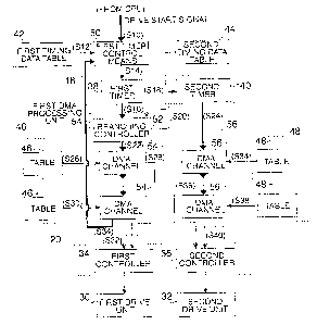
Fig. 2 is a function block diagram showing the
configuration of a first embodiment of the invention
together with a flow diagram of its operation. It should be
noted that in Fig. 2 and in each of the following figures of
comparable function block diagrams the DMA activation
operation is indicated by bold lines arid the data transfer
flow is indicated by fine lines.
As shown in Fig. 2 the control unit 20 of this
embodiment is composed of a first controller 34 and a second
controller 36. The first controller 34 and second controller
36 respectively control a first drive unit 30 and a second
drive unit 32. The first drive unit 30 is in this embodiment
a drive mechanism for driving a printer carriage, and the
second drive unit 32 is the print head of the printer, but
the invention shall not be so limited.
The timer unit 18 is composed of a first timer 38
corresponding to the first controller 34, and a second timer
40 corresponding to the second controller 36. The first
21
CA 02425347 2003-04-14
timer 38 and second timer 40 each have specific registers.
If timing data is written to these registers, the timers
output a time-up signal when the time specified by the
timing data passes.
The control apparatus 10 of this embodiment also has a
first timing data table 42, second timing data table 44,
first control data table 46, and second control data table
48.
Timing data for controlling the timing at which
operation of the first controller 34 and second controller
36 changes (more specifically, this data denotes the time
interval between the control change) is stored to first
timing data table 42 and second timing data table 44.
The first control data table 46 has "n" tables 46_1 to
46_n; "n" types of control data are stored by type to these
tables 46_1 to 46_n for controlling operation of the first
controller 34 at the respective control change times.
The second control data table 48 likewise has "m"
tables 48_1 to 48_m to which m types of control data are
stored by type for controlling operation of the second
controller 36 at the respective control change times.
Each of these tables 42, 44, 46_1 to 46_n, and 48_1 to 48_
are provided at a specific allocated address space in
memory 14, and the data stored to each table is set by the
CPU 12 before control starts.
The control apparatus 10 of this embodiment also has a
first timer control means 50, first DMA. processing unit 54,
and second DMA processing unit 56.
The first DMA processing unit 54 has a branching
controller 52 and "n" DMA channels 54_1 to 54_n corresponding
to the n-types of control data for the first controller 34.
The second DMA processing unit 56 has "m" DMA channels
56_1 to 56_m corresponding to the m-types of control data for
the second controller 36.
The first timer control means 50, branching controller
52, DMA channels 54_1 to 54_n, and DMA channels 56_1 to 56_",
constitute the DMA unit 16 shown in Fig. 1 and function as
independent DMA channels.
12
CA 02425347 2003-04-14
Fig. 3 shows the configuration and basic operation of
DMA. As shown in the figure each DMA channel has a transfer
source register R1, transfer destination register R2,
transfer count register R3, transfer method register R4, and
link destination register R5. The transfer source register
R1 and transfer destination register R2 are, respectively,
for storing the source address and the destination address
of the DMA transfer. The transfer count register R3 is for
storing the data transfer count for one activation (i.e.,
the number of data blocks transferred each time the channel
is activated). The transfer method register R4 stores the
method used for the data transfer, such as whether data is
transferred one byte at a time or by block unit. The link
destination register R5 is for declaring the DMA channel to
be activated when a DMA transfer process ends. That is, when
DMA starts the number of data bytes specified in transfer
count register R3 is transferred by the method specified in
transfer method register R4 from the source address stored
in transfer source register R1 to the destination address
stored in transfer destination register R2. When the data
transfer is completed, the DMA channel registered in link
destination register R5 (the "linked DMA channel" below) is
activated.
When data is transferred by DMA, the address values set
in transfer source register R1 and transfer destination
register R2 are automatically incremented to point to the
next memory address. Furthermore, the DMA registers R1 to R5
and the registers used by first timer 38 and second timer 40
are reserved at specific addresses in memory 14, and data is
written to the registers by transferring data to the
corresponding memory address.
The operation of this embodiment is described next with
reference to Fig. 2.
First, when a drive start signal is sent from the CPU
12 to the first timer control means 50 (S10), the first
timer control means 50 reads the first timing data from the
first timing data table 42 (S12) and passes the timing data
to the register of the first timer 38 (S14) . When the time
13
CA 02425347 2003-04-14
specified by the timing data passes after the timing data
is stored to its register, the first timer 38 sends a time
up signal to the branching controller 52 of the first DMA
processing unit 54 (S16).
The branching controller 52 is activated by the time-up
signal, reads the timing data from the second timing data
table 44 (S18), and transfers the timing data to the
register of the second timer 40 (S20). When this data
transfer is completed, the branching controller 52 activates
the linked DMA channel, that is, DMA channel 54_1 (S22). When
the time specified by the timing data passes after the
timing data is written to its register, the second timer 40
outputs a time-up signal to DMA channel 56_1 of the second
DMA processing unit 56 (S24) . As a result, DMA channel 56_1
is activated.
As thus described, DMA channel 54_1 of first DMA
processing unit 54 is activated by a start driving signal
from the CPU 12, and after the time specified by the timing
data then passes DMA channel 56_1 of second DMA processing
unit 56 is activated. First DMA processing unit 54 and
second DMA processing unit 56 thereafter handle DMA
transfers by means of DMA channels 54_1 to 54_r and DMA
channels 56_1 to 56_m.
More specifically, DMA channel 54_r activated by the
branching controller 52 in first DMA processing unit 54
reads the first control data from table 46_1 in first control
data table 46 (S26) and transfers it to the first controller
34 (S28). When this data transfer is completed DMA channel
54_2, which is the linked DMA channel of DMA channel 54_1, is
activated and reads and transfers the first control data
from table 46_2 to the first controller 34. This process
repeats until each DMA channel 54_; (where i <_ ~n) is
sequentially activated, reads the first control data from
table 46_i (S30) and transfers the control data to the first
controller 34 (S32), thus transferring n-different control
data to the first controller 34.
Likewise in the second DMA processing unit 56, the DMA
channel 56_1 activated by the second timer 40 reads the first
14
CA 02425347 2003-04-14
data from table 48_1 in the second control data table 48
(S34) and transfers it to the second controller 36 (S36).
When this data transfer is completed the DMA channel
56_2 that is the linked DMA channel of DMA channel 56_1 is
activated, reads the first control data from table 48_z and
transfers it to the second controller 36. This process
repeats until each DMA channel 56_i (where i <= m) is
sequentially activated, reads (S38) and transfers (S40) the
first control data from table 48_i to the second controller
36.
The first timer control means 50 is the linked DMA
channel of DMA channel 54_n in the first DMA processing unit
54, and when data transfer frcm DMA channel 54_n ends the
first timer control means 50 is restarted (S42). Therefore,
steps S12 to S40 described above repeat when the timing data
read from the first timing data table 42 by the first timer
control means 50 is transferred to the first timer 38.
Because the address of the transfer source register of each
DMA channel has been incremented at this time, r_ontrol data
of each type stored to each table is sequentially read and
passed along. When there is no more timing data to be read
next from the first timing data table 42 by the first timer
control means 50, the first timer control means 50 stops
operating and the data transfer sequence ends.
At the control timing specified by the timing data
stored to the first timing data table 42, the first DMA
processing unit 54 thus transfers the n-different control
data stored to the n tables 46_1 to 46_n of the first control
data table 46 one at a time by type to the first controller
34, and the first controller 34 then controls the first
drive unit 30 according to the received control data.
Furthermore, at the timing delayed a time defined by
the timing data stored in the second timing data table 44
from the data transfer timing of the first DMA processing
unit 54, the m-different control data stored to the m tables
48_1 to 48_~" in the second control data table 48 are
transferred one at a time by type by the second DMA
processing unit 56 to the second controller 36, and the
CA 02425347 2003-04-14
second controller 36 then controls the second drive unit 32
according to this received control data.
It will thus be apparent that as a result of the CPU 12
prestoring timing data and control data according to the
control operations to be achieved by the first controller 34
and second controller 36, this embodiment of the present
invention can, without imposing any load on the CPU 12,
precisely control the operation of a first drive unit 30 and
second drive ,unit 32 that are to run separate, mutually
synchronized processes.
It should be noted that control data is DMA transferred
to two controllers 34 and 36 due to the branching controller
52 of the first DMA processing unit 54 activating a second
DMA processing unit 56. The present invention shall not be
so limited, however, and control data can be transferred to
three or more control units within the range of usable DMA
channels by, for example, disposing a DMA device identical
to the branching controller 52 in the second DMA processing
unit 56 so that this DMA device activates yet another DMA
processing unit.
Furthermore, the first timer control means 50 is set as
the linked DMA channel of the last DMA channel 54_,~ in the
first DMA processing unit 54 in the embodiment described
above, and when data transfer by the last DMA channel 54_n
ends the next DMA processing cycle starts from the first
timer control means 50. The invention shall not be so
limited, however. For example, by setting the first timer
control means 50 as the linked DMA channel of the last DMA
channel 56_m in the second DMA processing unit 56, the
process cycle starting time of the first DMA processing unit
54 can be set referenced to the end time of data transfers
by the second DMA processing unit 56.
* Second embodiment
A second embodiment of the present invention is
described next. Fig. 4 is a function block diagram showing
16
CA 02425347 2003-04-14
the configuration of this second embodiment of the
invention together with the flow of its operation.
This embodiment applies the present invention to
printer control. A motor control unit 102 for controlling a
stepping motor 100 for driving a printer carriage
corresponds to the first controller 34 in the above first
embodiment, and a print head control unit 206 for
controlling a print head 104 corresponds to the second
controller 36 in the above first embodiment.
Furthermore, the first control data table 46 in this
embodiment is composed of a phase pattern table 108 and a
phase current table 110. The second control data table 48 is
composed of a print data table 112.
Yet further, the first DMA processing unit 54 is
composed of a phase pattern controller 116 and phase current
controller 118 as DMA channels. The second DMA processing
unit 56 is composed of a printing controller' 120 and a
second timer controller 122 as DMA channels.
The phase pattern controller 116 transfers the phase
pattern data stored in the phase pattern table 108 to the
motor control unit 102, and the phase current controller 118
transfers the phase current data stored in the phase current
table 110 to the motor control unit 102. The printing
controller 120 transfers print data from the print data
table 112 to the print head control unit 106. As further
described below print data for one pixel is transferred to
the print head control unit 106 as data denoting whether ink
is discharged in each plurally segmented ink discharge
period, and the print data is transferred synchronized to
each ink discharge period by the second timer controller 122
and third timer 124 activating the printing controller 120
based on the discharge timing data stored in the discharge
timing table 126.
In general the phase pattern of the voltage applied to
the motor must be sequentially changed in order to drive a
stepping motor. Therefore, the control timing data
indicating the timing for changing the phase of the stepping
motor 100 is defined in the first timing data table 42, and
17
CA 02425347 2003-04-14
the phase pattern data denoting the phase pattern of the
voltage to be applied to the stepping motor 100 at the
control timing is stored in the phase pattern table 108. It
is also necessary to change the phase current supplied to
the motor according to the drive control pattern when
driving the stepping motor 100, and the phase current data
denoting the phase current at each control timing is stored
in the phase current table 110.
Fig. 5 shows a typical example of the stepping motor
100 drive control pattern, Fig. 5 (a) showing the stepping
motor 100 speed pattern and (b) showing the current pattern
supplied to the stepping motor 100. When the stepping motor
100 is driven using a speed pattern with a trapezoidal
waveform as shown in Fig. 5 (a), a relatively high phase
current is supplied to accelerate the motor during
acceleration period I, a comparatively low phase current is
supplied in constant speed period II to overcome friction
and maintain a constant speed, and a high phase current is
then again supplied in deceleration period TII to produce
braking force and slow the motor. The CPU 12 sets the phase
current data at each control timing in the phase current
table 110 according to the phase current pattern determined
according to the drive control pattern of the stepping motor
100.
It should be noted that a constant current continues to
be supplied in period IV after the stepping motor 100 stops
so that a slight current is supplied in all phases of the
stepping motor 100 to rapidly attenuate residual stepping
motor 100 vibrations. This technique of energizing the motor
in all phases is referred to herein as supplying a steady
current. Therefore, after the stepping motor 100 reaches the
stop position, a steady current supply phase pattern (all
phases) and steady current level are defined as the last
control data, and the steady current supply time is set as
the last control timing data.
As in the first embodiment, the first DMA processing
unit 54 is activated at a timing determining by the control
timing data stored in the first timing data table 42, and
18
CA 02425347 2003-04-14
the control data stored in the phase pattern table 108 and
phase current table 110 are sequentially supplied one at a
time to the motor control unit 102. The stepping motor 100
is therefore controlled according to a drive pattern such as
shown in Fig. 5 (a) based on the data stored in these
tables.
In the present embodiment, however, the phase of the
stepping motor 100 changes each time the print head 104
prints one pixel. Then, as shown in Fig. 6, the ink
discharge period of the print head 104 for printing each
pixel is segmented into six divisions T1 to T6, for example,
and the density of each pixel can be controlled by the
printing controller 120 transferring the print data denoting
whether ink is charged or not in each division T1 to T6 to
the print head control unit 106 timed to each division T1 to
T6. In other words, the print data stored to the print data
table 112 is data declaring if the print head discharges ink
in each division Tl to T6 in which the print head can
discharge ink in order to print each pixel, and this print
data is transferred to the print head control unit 106 at
the timing corresponding to each division T1 to 'T6.
It should be noted that ink discharge is not limited to
the constant speed period and ink can be discharged during
acceleration and deceleration.
Furthermore, the number of segments into which each ink
discharge period is divided shall not be limited to six, and
any desired number of divisions could be used.
Because the phase of the stepping motor 100 is changed
each pixel, print data transfer in divisions T1 to T6 for
each pixel must be synchronized to the phase change timing
of the stepping motor 100. In this embodiment the branching
controller 52 starts the second timer 40 at the phase change
timing, and activates the printing controller 120 at the
time-up signal from the second timer 40. The second timer
controller 122 is activated after the data transfer by the
printing controller 120, and the discharge timing data
stored in the discharge timing table 126 (that is, the data
indicating the time length of divisions T1 to T6) is sent to
19
CA 02425347 2003-04-14
the third timer 124. The printing controller 120 is then
activated again at the time-up signal from the third timer
124. While synchronizing to the phase change timing of the
motor, the printing controller 120 thus transfers print data
for each pixel to the print head control unit 106 in each
division T1 to T6.
The operation of the present embodiment is described
next with reference to Fig. 4.
First, when a print start signal is sent from the CPU
12 to the first timer control means 50 (S50), the first
timer control means 50 reads the first timing data from the
first timing data table 42 (S52) and transfers it to the
first -timer 38 (S54) , When the time specified by the timing
data passes after the timing data is received, th.e first
timer 38 sends a time-up signal to the branching controller
52 (S56) .
The branching controller 52 is activated by the time-up
signal, reads the timing data from the second timing data
table 44 (S58), and transfers the timing data to the second
timer 40 (S60), When the data transfer is completed, the
branching controller 52 activates the phase pattern
controller 116, that is, the DMA destination (S62). When the
time specified by the timing data passes after the timing
data is received, the second timer 40 outputs a time-up
signal to printing controller 120 (S64), and the printing
controller 120 is thus activated.
The phase pattern controller 116 activated by the
branching controller 52 reads and transfers the first phase
pattern data from the phase pattern table 108 to the motor
control unit 102 (566, S68). When this data transfer is
completed the phase pattern controller 116 activates the
phase current controller 118, that is, the DMA destination
(S70): The activated phase current controller 118 transfers
the first phase current data from the phase current table
110 to the motor control unit 102 (572, S74).
When the phase pattern data and phase current data are
thus transferred to the motor control unit 102, the motor
control unit 102 controls the stepping motor 100 according
CA 02425347 2003-04-14
to this transferred data until the next control data is
received in the next DMA transfer cycle.
Furthermore, the printing controller 120 activated by
the second timer 40 transfers the first print data from the
print data table 112 to the print head control unit 106
(S76, S78) . When this data transfer is completed the second
timer controller 122, i.e., the DMA destination, is
activated (S80), and the discharge timing data is
transferred from the third timer 124 to the discharge timing
table 126 (582, S84). When the third timer 124 outputs the
time-up signal to the printing controller 120 (S86), the
printing controller 120 is activated again and the next
print data is transferred from the print data table 112 to
the print head control unit 106.
Transferring the print data for one pixel is completed
when the printing controller 120 completes this print data
transfer process six times. Ink is thus discharged in the
ink discharge period divisions specified by the print data
for each pixel, and each pixel is thus printed with the
desired density.
This embodiment of the invention thus prints at the
density specified for each pixel as a result of the phase
pattern data and phase current data being transferred to the
motor control unit 102 at the phase change timing specified
by the timing data stored in the first timing data table 42,
and the printing controller 120 then transferring the print
data in each division T1 to T6 to the print head control
unit 106 synchronized to each phase change timing.
Therefore, once a print start signal is applied to the
first timer control means 50 after the CPU 12 has stored
timing data, phase pattern data, and phase current data to
tables 42, 108, and 110 according to the drive control
pattern of the, stepping motor 100, and print data for each
pixel (data denoting whether ink is discharged in divisions
T1 to T6 according to the pixel density) has been written to
the print data table 112, this embodiment of the invention
can execute the printing operation without going through the
CPU 12.
21
CA 02425347 2003-04-14
In other words, this embodiment of the invention can
precisely execute two independent, mutually synchronized
processes, specifically controlling driving stepping motor
100 and controlling printed with a print head, without
imposing any load on the CPU 12.
It should be noted that in this second embodiment the
timing data stored to the second timing data table 44
specifies the time delay from the phase change timing to
when the printing controller 120 is. activated. Therefore, if
the printing position shifts in the carriage drive
direction, for example, the printing position can be
adjusted (the so-called left/right offset adjustment) by
setting the timing data appropriately.
This second embodiment has been described as a
monochrome printer with a single print head, but it will
also be obvious that the present invention could be applied
to a color printer having multiple print heads . That is, as
described in the first embodiment, the number of control
units for transferring control data by DMA can be increased
as needed to three or more so that a DMA processing unit
identical to the second DMA processing unit 56 is provided
for each print head controller and each print head can be
controlled as described above.
* Third embodiment
A third embodiment of the present invention is
described next. In this embodiment the first DMA processing
unit 54 in the configuration shown in the first embodiment
(see Fig. 2) can dynamically change the operation of the DMA
channels (that is, the content of the DMA control registers)
in the second DMA processing unit 56 during control
execution.
Fig. 7 is a function block diagram showing the
configuration of this third embodiment of the invention
together with the flow of its operation. As shown in the
figure the first DMA processing unit 54 of this embodiment
has a transfer count controller 200 as a DMA channel, and
22
CA 02425347 2003-04-14
the first control data table 4o accordingly has a transfer
count data table 202. Transfer count data specifying the
data transfer count of DMA channel 56_1 of the second DMA
processing unit 56 is stored to the transfer count data
table 202. When the transfer count controller 200 is
activated it transfers the transfer count data from the
transfer count data table 202 to the transfer count register
R3 in DMA channel 56_1. Therefore, when the first DMA channel
56_1 in second DMA processing unit 56 is activated, it
transfers the number of bytes corresponding to the transfer
count sent from the transfer count data table 202 to the
transfer count register R3.
The first DMA processing unit 54 in this embodiment of
the invention can thus change the amount of data transferred
by the DMA channel of the second DMA processing unit 56.
This means that if this embodiment is applied to printer
control, for. example, the first DMA processing unit 54 runs
a process for storing data received from a host computer to
a receive buffer, and the second DMA processing unit 56 runs
a process to output a specific number of pulses to the
output port at the data reception timing, the process run by
the second DMA processing unit 56 can be changed dynamically
from the first DMA processing unit 54 side so that, for
example, the number of pulses output by the second DMA
processing unit 56 changes according t:o the data received
from the first DMA processing unit 54 or pulse output is
even prohibited.
It will also be obvious that while changing the DMA
operation of one DMA channel 56_1 in the second DMA
processing unit 56 is varied in this third embodiment,
plural transfer count controllers 200 could alternatively be
provided to change the DMA operation of plural DMA channels
in the second DMA processing unit 56.
Furthermore, the DMA operation that is changed shall
not be limited to the transfer count. The transfer source
address, transfer destination address, transfer methods and
linked DMA channel could also be changed by appropriately
writing data to the corresponding control registers. For
23
CA 02425347 2003-04-14
example, the transfer count could .'oe changed for DMA
channel 56_1 while the transfer source address is changed
for DMA channel 56_2.
This third embodiment describes the first DMA
processing unit 54 changing the content of the DMA operation
of the second DMA processing unit 56, but a configuration in
which the second DMA processing unit 56 can change the
content of the DMA operation of the first DMA processing
unit 54 is also possible. Yet further, if the second DMA
processing unit 56 is configured to activate yet another DMA
processing unit, then the second DMA processing unit 56
could further change the content of the DMA operation of
that other DMA control unit.
* Fourth embodiment
A fourth embodiment of the present invention is
described next. Fig. 8 is a function block diagram showing
the configuration of this second embodiment of the invention
together with the flow of its operation.
This embodiment applies the present invention to
controlling an inkjet printer, and the first DMA processing
unit 54 controls a stepping motor 100 for driving a carriage
as in the second embodiment (Fig. 4). The second DMA
processing unit 56 has an ink data transfer means 302 for
DMA transfers of ink detection data from an ink detection
sensor 300 to memory.
The ink detection sensor 300 detects whether an ink
tank is loaded in the printer and whether there is any ink
in.the ink tank. Its output signal is AD converted by an AD
converter 303, and stored to a detection data register 304
as the ink detection data.
The ink data transfer means 302 of the second DMA
processing unit 56 transfers the ink detection data stored
in detection data register 304 to the ink detection data
buffer 306.
An error processing controller 308 detects if the ink
tank is not installed or there is no ink in the ink tank
24
8 CA 02425347 2003-04-14
based on the ink detection data stored to the ink detection
data buffer 306, and runs an appropriate process.
Fig. 9 is a schematic plan view showing the
configuration of an inkjet printer controlled by the present
embodiment and the location of the ink detection sensor 300.
As shown in this figure the printer carriage 310 is guided
by a guide shaft 314 and is driven right and left as seen in
the figure along the guide shaft 314 by the stepping motor
100. The print head 312 disposed to the carriage 310 prints
to a recording medium (referred to below as simply paper)
transported by a paper transportation unit 316.
Ink tanks 318 and 320 can be removably installed to the
printer. One ink tank 318 is a color ink cartridge holding
color ink, and the other ink tank 320 is a black ink
cartridge holding black ink. When the ink tanks 318 and 320
are installed both color ink and black ink are supplied
through ink tubes not shown in the figures to the print head
312.
Two detector prisms 324, 326 are disposed separated in
the carriage 310 movement direction on the side of ink tank
318 facing the carriage movement space 322. Similarly two
detector prisms 328, 330 are disposed separated in the
carriage 310 movement direction on the side of ink tank 320
facing the carriage movement space 322.
The ink detection sensor 300 is mounted on the side of
the carriage 310 facing the ink tanks 318 and 320, and thus
passes in front of the detection prisms 324, 326, 328, 330
in this order or reverse order when the carriage 310 is
driven left and right as seen in the figure. The ink
detection sensor 300 has a light-emitting part and a
photodetector part, and detects whether ink is in the ink
tanks 318 and 320 and whether the ink tanks 318 and 320 are
installed based on whether light is reflected from the
detector prisms 324 to 330.
Of these detector prisms 324 to 330, prisms 324 and 328
detect ink in the ink tanks 318 and 320. When the amount of
ink contained in the ink tanks 318 and 320 is greater than
or equal to a specific level, these detection prisms 324 and
CA 02425347 2003-04-14
328 are immersed in the ink and do not reflect incident
light from the ink detection sensor 300. When the in.k level
drops below this specific level, the prisms are exposed from
the ink and thus reflect incident light. The ink detection
sensor 300 can therefore detect whether ink is in the ink
tanks 318 and 320 based on whether reflection from the
detection prisms 324, 328 is detected.
Furthermore, detection prisms 326, 330 are disposed so
that they are exposed from the ink regardless of the ink
level in the ink tanks 318 and 320, and thus always reflect
incident light from the ink detection sensor 300. The ink
detection sensor 300 can therefore detect whether ink tank
318 or 320 is installed based on whether reflection is
detected from detection prism 326 or 330.
Fig. 10 shows an example of the voltage output signal
from the ink detection sensor 300 and the correlation
between the relative positions of the carriage 310 and
detector prisms 324 to 330. It should be noted that in this
example the output voltage drops when the photodetector of
the ink detection sensor 300 detects light. When both ink
tanks 318 and 320 are installed and there is ink in both ink
tanks, signals corresponding to detector prisms 324, 328 are
not detected as indicated by the solid line in the figure,
and signals A and B corresponding to detection prisms 326,
330 are output. When the ink in the ink tanks 318 and 320
drops below a specified level such that detector prisms 324,
328 are exposed, signals C and D corresponding to detector
prisms 324, 328 are also output as indicated by the dotted
lines in the figure.
As will be known from the signal waveforms shown in
Fig. 10, signals corresponding to detector prisms 324 to 330
are output only for a very small part of the entire period.
To minimize the memory capacity required in the ink
detection data buffer 306, it is therefore preferable to
store only the signals for the periods before and after
output of the signals corresponding to detector prisms 324
to 330 (i.e., the signals from periods I to IV in Fig. 10)
to the ink detection data buffer 306 as the ink detection
26
CA 02425347 2003-04-14
data. On the other hand, because periods I to IV are
determined by the movement of 'the carriage 310, the timing
for data transfers to the ink detection data buffer 306 must
be set based on the position of carriage 310 movement in
order to capture only the signals from periods I to IV.
As shown in Fig. 8 and described in the third
embodiment above, this embodiment of the invention therefore
disposes a transfer count controller 200 to the first DMA
processing unit 54 for controlling the stepping motor 100
that drives the carriage 310, and controls ink detection
data transfer by the ink data transfer means 302 by means of
the transfer count controller 200 transferring data from the
transfer count data table 202 to the transfer count register
R3 of the ink data transfer means 302.
Fig. 11 shows the data in the transfer count data table
202 of this embodiment correlated to the position of the ink
detection sensor 300 and the phase change timing of the
stepping motor 100. As shown in the figure, transfer control
data denoting whether transferring the ink detection data is
required (1 - required; 0 - not required) is stored in the
transfer count data table 202 correlated to the phase change
timing of the stepping motor 100. Note that the values in
the ranges corresponding to periods I to TV are 1.
As in the second embodiment the first DMA processing
unit 54 is activated at the phase change timing. The
transfer control data stored to the transfer count data
table 202 is therefore also transferred to the transfer
count register R3 of ink data transfer means 302 at the
phase change timing. If the value of the transfer control
data sent to the transfer count register R3 is l, the data
transfer count is also 1, and the ink data transfer means
302 transfers one byte of ink detection data from the
detection data register 304 to the ink detection data buffer
306. However, if the value of the transfer control data
written to the transfer count register R3 is 0, the data
transfer count is 0 and no data is transferred by the ink
data transfer means 302.
27
CA 02425347 2003-04-14
It should be noted that the output data from one
sensor is one byte long above, but if the sensor output
data is two bytes long the data transfer count passed when
data transfer is required is "2."
By controlling the number of bytes transferred by the
ink data transfer means 302 of the second DMA processing
unit 56 (or more specifically whether or not data is
transferred) according to the position of the carriage 310
controlled by the first DMA processing unit 54, the present
embodiment can thus transfer sensor output data to the ink
detection data buffer 306 only in the required periods I to
IV. This embodiment of the invention can therefore greatly
reduce the required memory capacity of the ink detection
data buffer 306 while enabling the error processing
controller 308 to efficiently determine if the ink supply is
depleted based on the ink detection data.
* Fifth embodiment
A fifth embodiment of the present invention is
described next. Fig. 12 is a function block diagram showing
the configuration of this fifth. embodiment of the invention
together with the flow of its operation.
In this embodiment the first DMA processing unit 54
stores data received by the printer from a host computer to
the receive buffer 420 of the first control unit 4~8.
The second DMA processing unit 56 respectively stores
the control commands and print data in the received data
stored to the receive buffer to the command buffer 424 and
image buffer 426 of the second control unit 422.
The first control unit 418 runs a specific control
process based on the received data stored to the receive
buffer 420. The second control unit 422 runs a specific
control process based on the data stored to the command
buffer 424 and image buffer 426.
Fig. 13 shows an example of data sent from a host
computer to a printer in this embodiment of the invention.
In the data train shown in this figure the value 00
28
CA 02425347 2003-04-14
indicates that the immediately following byte is a control
command, and the value 01 indicates that the follovaing byte
is print data. In this example, therefore, x1, x2, and x3
following the 00 values are interpreted as control commands,
and d1, d2, and so forth following O1 values are interpreted
as print data. The control commands following a received 00
are transferred to the command buffer 424, and print data
following a received 01 is transferred to the image buffer
426.
To achieve this operation the first DMA processing unit
54 has a received data transfer means 400, table transfer
means 402, and link destination transfer means 404 as DMA
channels. The second DMA processing unit 56 has as DMA
channels a switching controller 406, command transfer means
408, and data transfer means 410. Either the command
transfer means 408 or data transfer means 410 is set as the
linked DMA channel of the switching controller 406. Data
received by the printer from the host computer is stored to
the receive register 412.
When the received data transfer means 400 of the first
DMA processing unit 54 is activated by branching controller
52, the received data is transferred from the receive
register 412 to the receive buffer 420. The table transfer
means 402 then transfers the received data stored to the
receive buffer 420 to the table memory 416.
The table memory 416 outputs values determined by the
data written thereto to a specific output register 416a. As
shown in Fig. 14, the table memory 416 outputs DMA channel
number CH A for the command transfer means 408 in the second
DMA processing unit 56 when a 00 value denoting a control
command is received, and when a O1 value denoting print data
is received it outputs DMA channel number CH B for the data
transfer means 410 of the second DMA processing unit 56.
The link destination transfer means 404 then passes the
data written to the output register 416a to the link
destination register R5 of the switching controller 406 in
the second DMA processing unit 56. The link destination of
the switching controller 406 in the second DMA processing
29
CA 02425347 2003-04-14
unit 56 is therefore set to either the command transfer
means 408 or the data transfer means 410 according to the
value (00 or O1) of the received data.
The command transfer means 408 transfers data from the
receive buffer 420 to the command buffer 424, and the data
transfer means 410 transfers data from the receive buffer
420 to the image buffer 426. This means that only control
commands in the received data are stored to the command
buffer 424, and only print data in the received data is
stored to the image buffer 426.
Data transfers from the receive buffer 420 in the
present embodiment are thus executed by the table transfer
means 402, command transfer means 408, and data transfer
means 410, but when ane byte of data is transferred from the
receive buffer 420 by any one of these transfer means, the
transfer source address is incremented :in all three transfer
means. As a result, when 00 or O1 data indicating the data
type is transferred from the .receive buffer by the table
transfer means 402, the command transfer means 408 or data
transfer means 410 transfers the control command or print
data following the 00 or 01, respectively, and the table
transfer means 402 then transfers the next 00 or O1 data.
Because the table transfer means 402 thus always sends a 00
or O1 denoting the data type from the receive buffer 420 to
the table memory 416, values other than 00 or Ol will not be
transferred to the table memory 416.
Next, the data transfer process sending data from the
receive buffer 420 to the commarzd buffer 424 or image buffer
426 in the present embodiment is described more specifically
with reference to a case in which the data train shown in
Fig. 13 is stored to receive buffer 420. Note that the
transfer source address of the table transfer means 402 is
set to the first address in the receive buffer 420.
The table transfer means 402 first transfers the first
value, 00, of the received data to the table memory 416.
This causes the table memory 416 to output CH A
corresponding to 00 to the output register 416a. The link
destination transfer means 404 then transfers the address
CA 02425347 2003-04-14
CH A written to the output register 416a to the :link
destination register R5 of the switching controller 406 in
second DMA processing unit 56. The linked DMA channel of the
switching controller 406 is thus set to the command transfer
means 408. That is, when the command transfer means 408 is
activated after the switching controller 406, the second
received data unit, that is, the control command x1, is
transferred to the command buffer 424.
The fourth and sixth data units, i.e., control commands
x2 and x3, corresponding to the 00 value of the third and
fifth data units are likewise transferred to the command
buffer 424.
The address CH B is similarly output from the table
memory 416 due to the Ol value of the seventh and ninth data
units and written to the link destination register R5 of the
switching controller 406, thus activating the data transfer
means 410. The print data values d1 ancL d2 in the eighth and
tenth blocks are therefore transferred by the data transfer
means 410 to the image buffer 426.
Depending upon whether the data received by the first
DMA processing unit 54 is a control command or print data,
this embodiment of the invention thus changes the data
transfer destination of the second DMA processing unit 56 to
the command buffer 424 or the image buffer 426.
This embodiment has been described using two types of
received data, control commands and print data, by way of
example, but it will be obvious that there could three or
more types of received data. In this case DMA channels
corresponding to each of the handled data types are disposed
to the second DMA processing unit 5~ and the linked DMA
channel of the switching control means is set according to
the received data type to transfer data to buffers for each
type of data.
[Effects of the invention]
As described above, because a second DMA processing
unit for transferring control data to a second control unit
31
CA 02425347 2003-04-14
can be activated from a first DMA processing unit for
transferring control data to a first control unit, the
present invention can transfer control data independently to
first and second control units while s=ynchronizing the data
transfers. The present invention therefore enables more
complex control operations using direct memory access.
Although the present invention has been described in
connection with the preferred embodiments thereof with
reference to the accompanying drawings, it is to be noted
that various changes and modifications will be apparent to
those skilled in the art. Such changes and modifications are
to be understood as included within the scope of the present
invention as defined by the appended claims, unless they
depart therefrom.
32