Note: Descriptions are shown in the official language in which they were submitted.
CA 02425819 2003-04-17
ORGANIC LUMINESCENT COMPOUNDS AND
METHODS OF MAKING AND USING SAME
FIELD OF THE INVENTION
The invention relates to organic compounds having luminescent properties, and
to methods of
synthesizing and using such compounds. The invention more particularly relates
to compounds having
photoluminescent and/or electroluminescent properties, and to synthesis and
uses of same. The
invention also relates to compounds having photo-receptor properties due to
their ability to separate
charges. The invention also relates to compounds having photon harvesting
properties. The invention
also relates to compounds that visibly display detection of metal ions or
acid. The invention further
relates to compounds that can provide a molecular switch.
BACKGROUND OF THE INVENTION
Production of devices based on electroluminescent display is a rapidly
growing, billion dollar
industry. Bright and efficient organic light-emitting diode (OLED) devices and
electroluminescent (EL)
devices have attracted considerable interest due to their potential
application for flat panel displays
(e.g., television and computer monitors). OLED based displays offer advantages
over the traditional
liquid crystal displays, such as: wide viewing angle, fast response, lower
power consumption, and lower
cost. However, several challenges still must be addressed before OLEDs become
truly affordable and
attractive replacements for liquid crystal based displays. To realize full
color display applications, it is
essential to have the three fundamental colors of red, green, and blue
provided by emitters with
sufficient color purity and sufficiently high emission efficiency.
In general, when a potential is applied across an OLED, holes are said to be
injected from an
anode into a hole transporting layer (HTL) while electrons are injected from a
cathode into an electron
transporting layer (ETL). The holes and electrons migrate to an ETL/HTL
interface. Materials for
these transporting layers are chosen so that holes are preferentially
transported by the HTL, and
electrons are preferentially transported by the ETL. At the ETL/HTL interface,
the holes and electrons
recombine to give excited molecules which radiatively relax, producing an EL
emission that can range
from blue to near-infrared (Koene, 1998).
In providing one of the key color components for electroluminescent display
devices, blue
luminescent compounds are among the most sought-after materials by industry
around the world. Two
alternative ways in which blue luminescence can be achieved are: (1) providing
a molecule which emits
1
CA 02425819 2003-04-17
blue color (emitter), and {2) doping an emitter such that the combination
yields blue luminescence.
Conveniently, the emitter can be an inorganic metal ion such as, for example,
lanthanide, which emits
blue light via d to f or f to f electronic transitions, or an organic molecule
which has conjugated n bonds
and emits blue light via 7z to 7z or ~ to n electronic transitions.
t~ common problem with blue emitters is their lack of long term stability in
OLEDs. OLEDs
generally suffer from a gradual intensity decrease o.f the blue hue, which
results in gradual deterioration
of the color purity of the display, and ultimately failure of the device.
Television and computer monitors
must perform consistently for at least five years in order to be commmercially
feasible. Even this
modest expectation is a big challenge for currently available OLEDs.
There are several blue luminescent inorganic coordination compounds known
(U.S. Patent No.
6,500,569, U.S. Patent No. 6,312,835, Wang, 2001, Jia et al., 2003); however,
in some cases, due
to a propensity for oxidation and/or hydrolysis reactions, such complexes are
not very stable in solution.
One family of known inorganic blue emitters; lanthanide ions, have low
emission efficiency and require
the use of a host (generally an inorganic salt), which makes it difficult to
process them into thin films.
1 S Thus, blue luminescent materials that are organic in nature are desirable
due to their increased
stability, solubility and ability to form thin films. A number of organic blue
emitters are known to date
(Shirota, 2000, Wang, 2001). Many of these have poor luminescence efficiency
and poor stability.
Some are luminescent polymers that are difficult to apply in films using
chemical vapor deposition
(CVD) or vacuum deposition, processes known to produce superior films for
electroluminescent
displays. Even the best blue emitters currently available do not have the long
term stability desired for
commercial devices.
The limitations discussed above could restrict the market for OLED products,
despite their
many superior aspects as compared with liquid crystal displays. Therefore, in
order f~r OLEDs to
become truly feasible, there is a need for stable, organic emitters.
BRIEF STATEMENT OF THE INVENTION
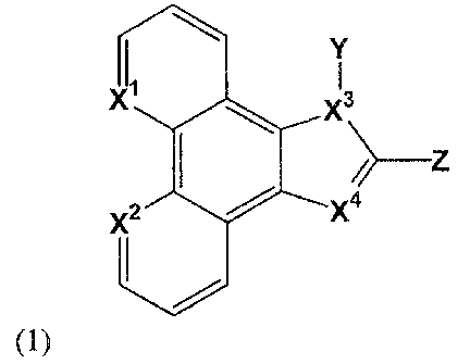
In a first aspect, the invention provides a compound having a formula (1)
2
CA 02425819 2003-04-17
Y
I3
X/4
(1)
where X', X2, X3 and X4 are each independently selected from the group
consisting of carbon and
nitrogen; Y is selected from the group consisting of hydrogen, a substituted
or unsubstituted aryl group,
and a substituted or unsubstituted aliphatic group having 1-24 carbon atoms
which rnay be straight,
branched or cyclic; Z is a substituted or unsubstituted aryl moiety selected
from the group consisting of
phenyl, biphenyl, naphthyl, anthryl, phenanthryl, pyrenyl, pyridyl, bipyridyl,
indyl, and quinolinyl; and
wherein a said substituent is selected from the group consisting of an aryl
group, an alkoxy group, a
hydroxy group, a halo group, an amino group, a nitro group, a nitrite group, -
CF3 and an aliphatic
group having 1-24 carbon atoms which may be straight, branched or cyclic. The
compound is
preferably photoluminescent or electroluminescent.
X', XZ, X3 and X4 may be independently selected from the group consisting of a
substituted
carbon, an unsubstituted carbon and an unsubstituted nitrogen. In some
embodiments, at least one of
X', X2, X3 and X4 may be nitrogen. In some embodiments, all of X', X2, X3 and
X4 may be nitrogen.
Y may be an aliphatic group having 1-12 carbon atoms. In a preferred
embodiment, Y may be
an aliphatic group having 1-4 carbon atoms.
In a second aspect, the invention provides a method of synthesizing a compound
of said first
aspect, comprising at least one step selected from the group consisting of
Phen(NHZ)Z + ZCOOH ~ PhenImZ
and PhenImZ + NaH + YI ~ YPhenImZ
wherein Y is selected from the group consisting of hydrogen, substituted or
unsubstituted aryl
group, and substituted or unsubstituted aliphatic group having 1-24 carbon
atoms which may be
straight, branched or cyclic; Z is selected from the. group consisting of
phenyl, biphenyl, naphthyl,
3
CA 02425819 2003-04-17
anthryl, phenanthryl, pyrenyl" pyridyl, bipyridyl, indyl, and quinolinyl; and
wherein a said substituent is
selected from the group consisting of an aryl group, an alkoxy group, a
hydroxy group, a halo group, an
amino group, a vitro group, a nitrite group, -CF3 and an aliphatic group
having 1-24 carbon atoms
which may be straight, branched or cyclic.
In a third aspect, the invention provides a method of synthesizing a compound
of said first
aspect comprising at least one step selected from the group consisting of
Phen02 + ZCHO ~1 PhenImZ
and PhenImZ + NaH + YI -~ YPhenhnZ
wherein Y is selected from the group consisting of hydrogen, substituted or
unsubstituted aryl
group, and substituted or unsubstituted aliphatic group having 1-24 carbon
atoms which may be
straight, branched or cyclic; Z is selected from the group consisting of
phenyl, biphenyl, naphthyl,
anthryl, phenanthryl, and pyrenyl; and wherein a said substituent is selected
from the group consisting of
an aryl group, an alkoxy group, a hydroxy group, a halo group, an amino group,
a vitro group, a nitrite
group, -CF3 and an aliphatic group having 1-24 carbon atoms which may be
straight, branched or
cyclic.
In other aspects, the invention provides a photoluminescent or
electroluminescent compound
having a formula selected from the group consisting of PhenImAn (2),
MePhenImAn (3), PhenImPy
(4), and MePhenImPy (S).
In another aspect, the invention provides a composition comprising a compound
of general
formula (1), an organic polymer and a solvent. In a further aspect, the
invention provides a composition
comprising a photoluminescent or electroluminescent compound of general
formula (1), an organic
polymer and a solvent.
In another aspect, the invention provides a photoluminescent product or an
electroluminescent
product comprising a compound of general formula (1). The product may be a
flat panel display
device. It may be a luminescent probe.
In yet another aspect, the invention provides a method of producing
electroluminescence,
comprising the steps of providing an electroluminescent compound of general
formula (1) and applying
a voltage across said compound so that said compound electroluminesces.
In a further aspect the invention provides an electroluminescent device for
use with an applied
voltage, comprising: a first electrode, an emitter which is an
electroluminescent compound of general
formula (1), and a second, transparent electrode, wherein voltage is applied
to the two electrodes to
produce an electric field across the emitter so that the emitter
electroluminesces.
4
CA 02425819 2003-04-17
In a still further aspect, the invention provides an electroluminescent device
for use with an
applied voltage, comprising: a first electrode, a second, transparent
electrode, an electron transport
layer adjacent the first electrode, a hole transport layer adjacent the second
electrode, and an emitter
which is an electroluminescent compound of general formula (1) interposed
between the electron
transport layer and the hole transport layer, wherein voltage is applied to
the two electrodes to produce
an electric field across the emitter so that the emitter electroluminesces.
In another aspect, the invention provides a method of detecting metal ions
comprising the steps
of: providing a photoluminescent compound of general formula (1), and
detecting photoluminescence
of said compound, wherein contact with a metal ion quenches said
photoluminescence of said
compound. The metal ions may be selected from the group consisting of Zn2+,
Cuz+ and lViz+
In yet another aspect, the invention provides a method of detecting acid
comprising the steps of
providing a photoluminescent compound of general formula (1), and detecting
photoluminescence of
said compound, wherein protonation of said compound changes the state of said
compound's
photoluminescence.
In another aspect, the invention provides a method of harvesting photons
comprising the steps
of providing a compound of general formula (1), and providing light such that
photons strike said
compound and charge separation occurs in said compound. The separated charges
may recombine
and photons be released. Alternatively, the separated charges may migrate to
respective electrodes to
produce a potential difference.
, In another aspect, the invention provides a method of separating charges
comprising the steps
of providing a compound of general formula (1) and providing light such that
photons strike said
compound and charge separation occurs in said compound. The separated charges
may recombine
and photons be released. Alternatively, the separated charges may migrate to
respective electrodes to
produce a potential difference.
In respective further aspects, the invention provides a photocopier, a
photovoltaic device, a
photoreceptor, a solar cell and a semiconductor employing the afore-mentioned
method of harvesting
photons or the afore-mentioned method of separating charges.
In a still further aspect, the invention provides a molecular switch
comprising a compound of
general formula (1) that is capable of existing in more than one luminescent
state, wherein acid, base,
and/or incident light produces a change in the luminescent state of said
compound. In certain
embodiments, said compound may be 2-(9-anthryl)imidazo[4,5-f]-[
1,10]phenanthroline (2) or 2-(2-
pyridyl)imidazo[4,5-f]-[1,10]phenanthroline (4).
S
CA 02425819 2003-04-17
In another aspect, the invention provides a circuit comprising a said
molecular switch.
BRIEF DESCRIPTION OF THE DRA~VII\TGS
For a better understanding of the present invention and to show more clearly
how it may be
carried into effect, reference will now be made by way of example to the
accompanying drawings,
which illustrate aspects and features according to preferred embodiments of
the present invention, and
in which:
Figure 1 shows a preferred embodiment of a three layer electroluminescent (EL)
display device
according to the invention;
Figure 2 shows the luminescence spectra of PhenImAn (2) in DMF (0~~), 'rHF
(eoo) and
methylene chloride (-) at a concentration of 1.0 x 10⁻⁵ M;
Figure 3 shows the luminescence spectra of MePhenImAn (3) in DMF (~~~), THF
(ano) and
methylene chloride (-) at a concentration of 1.0 x 10⁵ M;
Figure 4 shows the luminescence spectra of PhenImPy (4) in DMF (~~~), THF
(ooo) and
methylene chloride (-) at a concentration of I.0 x 10-5 M;
Figure 5 shows the luminescence spectra of MePhenImPy (5) in DMF (~~Cl), THF
(men) and
methylene chloride (-) at a concentration of 1.0 x 10⁻⁵ M;
Figure 6 shows the change of the luminescence spectra of MePhenImAn (3) in
DMF, at a
concentration of 1.0 x 10⁻⁵ M with the addition of Zn(OAc)2 at a concentration
of 1.0 x 10'3 M at
298K;
Figure 7 shows the change of emission intensity of MePhenImAn (3) in DMF at a
concentration
of 1.0 x 10'5 M at 478 manometers with the addition of Zn(OAc)Z in DMF at a
concentration of 1.0 x
10-3 M at 298K;
Figure 8 shows the change of emission intensity of PhenImAn (2) in DMF at a
concentration of
2.5 x 10~ M with the addition of 0 equivalents (~~L7), and S equivalents (-)
of H+ added as aqueous
HCl at 298K;
Figure 9 shows the change of emission intensity of PhenImPy (4) in DMF, 7~",~
369 nm at a
concentration of 2.5 x 10~' M with the addition of 0 equivalents (--), 0.20
equivalents (0~0) and 5
equivalents (-) of H+ added as aqueous HCI at 298K;
Figure 10 shows photoluminescence (7~,r,aX = 475 nm) and electroluminescence
(~max = 505 nm) spectra for MePhenImAn (3) in a three layer device described
in Example 5;
6
CA 02425819 2003-04-17
Figure 11 shows a plot of current versus voltage that displays the
electroluminescent efficiency
obtained with MePhenImAn (3) in the device of Figure 10;
Figure 12 shows a plot of luminance versus current that displays the
brightness of the
electroluminescence produced by device of Figures 10 and 11;
Figure 13 shows the crystal structure of PhenImAn (2);
Figure 14 shows the crystal structure of MePhenImAn (~); and
Figure 15 shows the crystal structure of [Zn(MePhenImAn)(Ac0)z(H20)~.
7
CA 02425819 2003-04-17
DETAILED DESCRIPTION OF THE IN'~ENTION
In a first aspect of the invention, a stable organic compound of the general
formula (1) is
provided:
Y
s
(1) ~Z
~,4
where X', X2, X3 and X4 are each independently selected from the group
consisting of carbon and
nitrogen;
Y is selected from the group consisting of hydrogen, substituted or
unsubstituted aryl group, and
substituted or unsubstituted aliphatic group having 1-24 carbon atoms which
may be straight, branched
or cyclic;
Z is a substituted or unsubstituted aryl moiety selected from the group
consisting of phenyl,
biphenyl, naphthyl, anthryl, phenanthryl, pyrenyl, pyridyl, bipyridyl, indyl,
and quinolinyl (preferred
substituent examples la-lm are pictured below); and
wherein a said substituent is selected from the group consisting of an aryl
group, an alkoxy
group, a hydroxy group, a halo group, an amino group, a vitro group, a nitrite
group, -CF3 and an
aliphatic group having 1-24 carbon atoms which may be straight, branched or
cyclic.
As used herein "aliphatic" includes alkyl, alkenyl and alkynyl. An aliphatic
group may be
substituted or unsubstituted. It may be straight chain, branched chain or
cyclic.
Preferably a compound of formula (I) exhibits intense luminescence, which may
be
photoluminescence and/or electroiuminescence. Preferably, Y is 1-4 carbon
atoms.
8
CA 02425819 2003-04-17
/ \
/I
la 1-naphthyl Ik~ 2-naphthyl
1c 9-anthryl
1e 1-pyrenyl if Z-pyrenyl i~ ~-pyrenyl
16 biphenyl li phenyl
9
ld 9-phenanthryi
CA 02425819 2003-04-17
lj indyl lk quinolinyl
N, // ~ ,N
11 pyridyl lm ~4, 4'-bipridyl
1~
CA 02425819 2003-04-17
In preferred embodiments, X', XZ, X3 and X4 are each independently a
substituted or
unsubstituted carbon (an unsubstituted carbon has hydrogen as its
substituent(s)) or an unsubstituted
nitrogen. In some embodiments, one, two or three of X', XZ, X3 and X4 are
nitrogen. In a preferred
embodiment, X', X2, X3 and X4 are all nitrogen. A synthetic scheme depicting
the preparation of such
compounds is pictured in Schemes 1 and 2; working examples of detailed
synthetic procedures are
provided in Examples 1-4.
Scheme 1. Preparation of precursors for Scheme 2.
N
KBr(s), HZS04/HN03
100°C, 4 h
N
HONH2 HCl, BaC03(s)
.
EtOH, reflux, 30 min
NZH~, 10% PdC
EtOH, reflux, 12 h
11
CA 02425819 2003-04-17
Scheme 2. Preparation of compounds of the general formula (1).
O
O Z'CHO
Glacial HOAc
reflux, 4hr
H 1~ \ Y
\ N 1 ) NaH(s) / DMF, RT \ N
Z 2) YI, RT, overnight
ZZCOOH
PPA, 230°C
reflux, 4hr
wherein Y is selected from the group consisting of hydrogen, substituted or
unsubstituted aryl
group, and substituted or unsubstituted aliphatic group having l -24 carbon
atoms which may be
straight, branched or cyclic;
Z' is selected from the group consisting of substituted or unsubstituted
phenyl, biphenyl,
naphthyl, anthryl, phenanthryl, and pyrenyl;
Z2 is selected from the group consisting of Z', substituted or unsubstituted
pyridyl, bipyridyl,
indyl, and quinolinyl; and
wherein a said substituent is selected from the group consisting of an aryl
group, an alkoxy
group, a hydroxy group, a halo group, an amino group, a vitro group, a nitrile
group, -CF3 and an
aliphatic group having 1-24 carbon atoms which may be straight, branched or
cyclic.
In some embodiments, Y is an aliphatic group having 1-12 carbons. In some
embodiments, Y
is an aliphatic group having 1-4 carbons.
In yet another embodiment, this aspect of the invention provides compounds
wherein X', X2,
1 S X3 and X4 are each carbon. Preparation of precursors that are analogous to
those in Scheme 1 but in
which X', X2, X3 and X4 are each carbon is described in Yamazaki, 2001. Such
precursors can then
12
CA 02425819 2003-04-17
be reacted according to Scheme 2.
Thus, the invention provides, for example, compounds PhenImAn (2), MePhenImAn
(3),
PhenImPy (4), MePhenImPy (5), which have the following structures:
I3
CA 02425819 2003-04-17
PhenImAn: 2-(9-anthryl)imidazo~~.,5-~-1,10]phenanthroline (2)
(2)
14
CA 02425819 2003-04-17
MePhenImAn: 1-methyl-2-(9-anthryl)imidazo[4,5-fj-1,10]phenanthroline (3)
(3)
CA 02425819 2003-04-17
PhenImPy: 2-(2-pyridyl)imidazo[4,5-fJ-[1,10]-phenanthroline (4)
(4)
1G
CA 02425819 2003-04-17
MePhenImPy: 1-methyl-2-(2-pyridyl)imidazo[4,5-fJ-[1,10]-phenanthroline (5)
{5)
17
CA 02425819 2003-04-17
The invention provides compounds that are photoluminescent and, in at least
some
embodiments of the invention, electroluminescent; they can produce intense
light.
The invention also provides a method of producing photoluminescence comprising
the steps of
providing a photoluminescent compound of the invention having a formula as set
out above; and
irradiating said photoluminescent compound with radiation of a wavelength
suitable for exciting the
compound to photoluminescence.
The invention further provides a method of producing electroluminescence
comprising the steps
of providing an electroluminescent compound of the invention having a formula
as set out above; and
applying a voltage across said electroluminescent compound.
The invention further provides an electroluminescent device for use with an
applied voltage,
comprising: a first electrode, an emitter (e.g., phosphor) which is an
electroluminescent compound of
the invention, and a second, transparent electrode, wherein a voltage is
applied between the two
electrodes to produce an electric field across the emitter. The emitter
consequently electroluminesces.
In some embodiments of the invention, the device includes one or more charge
transport layers
interposed between the emitter and one or both of the electrodes. For example,
spacing of a preferred
embodiment of the device, called for the purposes of the present specification
a "three layer EL
device", is: first electrode, first charge transport layer, emitter, second
charge transport layer, and
second, transparent electrode.
A particularly preferred compound according to this aspect of the invention,
which has been
shown to exhibit blue photoluminescence and blue electroluminescence, is
MePhenImAn (3) , for which
a preferred synthetic protocol is described in Example 2. Example 5, referring
to Figures 10-12,
describes photoluminescence and electroluminescence work on this compound
employing a device
made and operated at Xerox Research Centre of Canada (Mississauga, Ontario).
An advantage of preferred luminescent compounds of th.e invention is that they
are highly
soluble in common organic solvents such as toluene, diethyl ether,
tetrahydrofuran (THF), and
dichloromethane. This permits the compounds to be blended easily and
conveniently with organic
polymers. The role of the organic polymer in such a mixture is at least two-
fold: First, a polymer can
provide protection for the luminseent compound from air degradation. Second, a
polymer host matrix
permits the use of a spin-coating or dip-coating process as an alternative way
to make luminescent
films. Although spin-coating and dip-coating processes may not produce as high
quality films as those
produced by chemical vapor deposition or vacuum deposition, they are often
much faster and more
economical.
1$
CA 02425819 2003-04-17
Accordingly, the invention further provides methods of applying compounds as
described
above to a surface. These methods include solvent cast from solution,
electrochemical deposition,
vacuum vapor deposition, chemical vapor deposition, spin coating and dip
coating. The compounds
may be applied alone or with a carrier. In some embodiments of the invention,
they are applied in a
composition including an organic polymer. Such compositions are also
encompassed by the invention.
As an example of this application, the lVIePhenImPy (5) compound forms a clear
transparent
solution with the weakly-luminescent polymer poly(N vinylcarbazole) (PVK) in
CI-IZC12/C6H5Cl. This
can be converted to a transparent film by evaporating the toluene solvent via
either a dip-coating or
spin-coating process. Luminescent films obtained in this way are stable.
Certain polymers such as, for
example, PVK, are expected to further enhance the luminescence of the emitter
in the film.
Conveniently, spin coating may be performed using a Chemat Technology spin-
water KW-4A; and
vacuum deposition may be performed using a modified Edwards manual diffusion
pump.
The invention provides a method of producing electroluminescence comprising
the steps of
providing an electroluminescent compound of the invention having the general
formula (1) as set out
above; and applying a voltage across said electroluminescent compound so that
the compound
electroluminesces.
According to the invention, electroluminescent devices for use with an applied
voltage are
provided. In general, such a device has a first electrode, an emitter which is
an electroluminescent
compound of the invention, and a second, transparent electrode, wherein a
voltage is applied between
the two electrodes to produce an electric field across the emitter of
sufficient strength to cause the
emitter to electroluminesce. Preferably, the first electrode is of a metal,
such as, for example, aluminum,
which reflects light emitted by the compound; whereas the second, transparent
electrode permits
passage of emitted light therethrough. The transparent electrode is preferably
of indium tin oxide (IT~)
glass or an equivalent known in the art. Here, the first electrode is the
cathode and the second
electrode is the anode.
Referring to Figure 1, a preferred embodiment of an electroluminescent device
of the invention
is shown. The emitter is interposed between an electron transport layer (e.g.,
tris-(8-
hydroxyquinoline)aluminum (Alq3) or 2-(biphenyl-4-yl)-5-(4-tent-butyl phenyl)-
1,3,4-oxadiazole
(PBD)) adjacent the first metal electrode and a hole transport layer (e.g.,
N,lVy-di-1-naphthyl-N,1V'-
diphenylbenzidiine (NPB)) adjacent the second, transparent electrode. The
choice of the materials
employed as charge transport layers will depend upon the specific properties
of the particular emitter
employed. The hole transport layer or the electron transport layer may also
function as a supporting
19
CA 02425819 2003-04-17
layer. The device is connected to a voltage source such that an electric field
of sufficient strength is
applied across the emitter. Light, preferably blue light, consequently emitted
from the compound of the
invention passes through the transparent electrode.
In some embodiments of the invention, the device includes one or more charge
transport layers
interposed between the emitter and one or both of the electrodes. Such charge
transport layers) are
employed in prior art systems with inorganic salt emitters to reduce the
voltage drop across the emitter.
In a first example of such a device, layers are arranged in a sandwich in the
following order: first
electrode, charge transport layer, emitter, second charge transport Layer, and
second transparent
electrode. In a preferred embodiment of this type, a substrate of glass,
quartz or the like is employed.
A reflective metal layer (corresponding to the first electrode) is deposited
on one side of the substrate,
and an insulating charge transport layer is deposited on the other side. The
emitter layer which is a
compound of the invention is deposited on the charge transport layer,
preferably by vacuum vapor
deposition, though other methods may be equally effective. A transparent
conducting electrode (e.g.,
ITO) is then deposited on the emitter layer. An effective voltage is applied
to produce
electroluminescence of the emitter.
In a second example of an EL device of the invention a second charge transport
layer is
employed, and the sandwich layers are arranged in the following order: f rst
electrode, first charge
transport layer, emitter, second charge transport layer and second,
transparent electrode.
Electroluminescent devices of the invention may include one or more of the
blue-emitting
compounds described herein. In some embodiments of the invention, an
electroluminescent device
such as a flat panel display device may include not only a blue-emitting
phosphor as described herein,
but may be a multiple-color display device including one or more other
phosphors. The other
phosphors may emit in other light ranges, e.g., red, green, and/or be
"stacked" relative to each other.
Convenient materials, structures and uses of electroluminescent display
devices are described in Rack
et al., 1996.
For photoluminescence, the compounds absorb energy from ultraviolet radiation
and emit
visible light near the ultraviolet end of the visible spectrum e.g., in the
blue region. For
electroluminescence, the absorbed energy is from an applied electric field.
The luminescence of, for
example, PhenImAn (2) and MePhenImAn (3) can be readily quenched by the
addition of acid or
metal canons such as Zn2+, Cu2+, Ni2~'and ~I+. For example, when Zn(Ac0)2 is
added to a
dimethylformamide (DMF) solution of MePhenImAn (3), the bright blue
luminescence of the solution
changes gradually to very weak yellow:
CA 02425819 2003-04-17
MePhenImAn + Zn(Ac0)2 ~ Zn(MePhenlmAn)(Ac0)2
(Bright Blue) (Weak Yellow)
The quenching process is shown in Figure 6 and Figure 7, which indicate the
formation of a 1
metal:ligand (L) complex, as confirmed by x-ray single crystal structure
analysis shown in Figure 15.
The invention further provides methods employing compounds of the invention to
harvest
photons, and corresponding devices for such use. Spectroscopic studies have
demonstrated that
compounds of the invention have high efficiency to harvest photons and produce
highly polarized
electronic transitions. In general, when such compounds are excited by light,
a charge separation occurs
within the molecule; a first portion of the molecule has a negative charge and
a second portion has a
positive charge. Thus the first portion acts as an electron donor and the
second portion as an electron
acceptor. If recombination of the charge separation occurs, a photon is
produced and luminescence is
observed. In photovoltaic devices, recombination of the charge separation does
not occur; instead the
charges move toward an anode and a cathode to produce a potential difference,
from which current
can be produced.
Molecules with the ability to separate charges upon light initiation are
useful for applications
such as photocopiers, photovoltaic devices and photoreceptors. Organic
photoconductors provided
by the present invention are expected to be useful in such applications, due
to their stability and ability
to be spread into thin films. Related methods are encompassed by the
invention.
Organic semiconducting materials can be used in the manufacture of
photovoltaic cells that
harvest light by photoinduced charge separation. To realize an efficient
photovoltaic device, a large
interfacial area at which effective dissociation of excitons occurs must be
created; thus an electron
donor material is mixed with an electron acceptor material. (Here, an exciton
is a mobile combination
of an electron and a hole in an excited crystal, e.g., a semiconductor.)
Organic luminescent
compounds as semiconductors are advantageous due to their long lifetime,
efficiency, low operating
ZS voltage and low cost.
Photocopiers use a light-initiated charge separation to attract pasitively-
charged molecules of
toner powder onto a drum that is negatively charged.
The invention further provides methods employing compounds of the invention to
detect metal
ions. As an example, Figure 14 shows the change in emission intensity of
MePhenIrnAn (3) with the
addition of Zn2+. The change in the luminescence upon coordination of metal
ions may be useful for
detection of gunpowder residue, bomb making activity, and/or environmental
contamination such as
heavy metal contamination of food or soil or water, as well as for detection
of sites of meteor impact
21
CA 02425819 2003-04-17
and even interplanetary exploration.
The invention further provides methods employing compounds of the invention to
detect acid.
As an example, Figure 8 and Figure 9 show the change in the emission intensity
of PhenImAn (2) and
PhenlmPy(4), respectively, with the addition of 5 equivalents of acid. This
aspect of the invention is
expected to be useful for a variety of applications, including, without
limitation, pH sensors, as well as
detection of contamination, particularly environmental contamination (e.g.,
acidity of lakes, soil, etc.).
The invention further provides molecular switches employing compounds as
described above,
and methods of use thereof. In a preferred embodiment, the compounds PhenImAn
(2) and PhenImPy
(4} are employed. These compounds can exist in three different states
(protonated, neutral and
deprotonated).
Information processing systems of current computers are based on semiconductor
logic gates
or switches (Tang et al.,1987). By reducing the switching elements to a
molecular level, the processing
capability and memory density of computers could be increased. by several
orders of magnitude and the
power input could be decreased significantly (Leung et al., 2000). Candidates
for this purpose are
molecules that are capable of undergoing reversible transformations in
response to chemical, electrical
and/or optical stimulation, and producing readily detectable optical signals
in the process. For example,
the respective neutral forms of PhenImAn (2) and PhenImPy (4), when in
solution, emit blue
luminescence. The neutral forms can be easily converted to the non-luminescent
protonated forms by
the addition of acid. These can be switched back to the depronated forms by
the addition of a base.
Three-state molecular circuits based on PhenImAn (2) and PhenImPy (4) with OH-
, H+ and ultraviolet
light as inputs and visible light as outputs have been established.
Examples 1 to 4 below provide detailed descriptions of the syntheses of
compounds (2),
(3},(4), and (S), respectively. As would be apparent to a person of ordinary
skill in the art, other
functionalities may be included in derivatives according to the invention.
Alternatively, starting materials
may be modified to include, but are not limited to, functionalities such as
ether, epoxide, ester, amide or
the like. Such functionalities may in some cases confer desirable physical or
chemical properties, such
as increased stability or luminescence.
WORKING EXAli~IPLES
All starting materials were purchased from Aldrich Chemical Company and used
without further
purification. Solvents were freshly distilled over appropriate drying
reagents. All experiments were
carried out under a dry nitrogen atmosphere using standard Schlenk Techniques
unless otherwise
stated. Thin Layer Chromatography was carried out on Si02 (silica gel F254,
Whatrnan). Flash
22
CA 02425819 2003-04-17
chromatography was earned out on silica (silica gel 60, 70-230 mesh). 'H
and'3C spectra were
recorded on a Bruker Avance 300 spectrometer operating at 300 and 75.3 MHz
respectively.
Excitation and emission spectra were recorded on a Photon Technologies
International QuantaMaster
Model 2 spectrometer. Data collection for the X-ray crystal structural
determinations were performed
on a Bruker SMART CCD 1000 X-ray diffractometer with graphite-monochromated Mo
Ka radiation
(~. = 0.71073 t~) at 298K and the data were processed on a Pentium PC using
the Bruker AXS
Windows NT SHELXTL software package (version 5.10). Elemental analyses were
performed by
Canadian Microanalytical Service Ltd., (Delta, B.C., Canada). Melting points
were determined on a
Fisher-Johns melting point apparatus.
Though not specifically described in the working examples set forth below,
conveniently EL
spectra may be obtained using Ocean Optics HR2000; and data involving current,
voltage and
luminosity may be obtained using a Keithley 238 high current source measure
unit.
Example 1: Synthesis of PhenImAn (2). 3.0 mmol of Phendione, 60 mmol of
NH4Ac(s) and
3.3 mmol of 9-anthrylaldehyde were added to 100 mL glacial acetic acid and the
mixture was refluxed
for 4 hours under NZ(g) . The mixture was then cooled to room temperature and
500 mL of water was
added with stirring. A dark yellow solid was obtained immediately. The solid
was then collected by
filtration and washed thoroughly with water and then acetone. The product
PhenImAn (2) was dried in
vacuo and was obtained at 82% yield. 'H Nuclear Magnetic Resonance (NMR) (500
MegaHertz
(MHz), d4-methanol, -50°C, referenced to tetramethylsilane (TMS)):
chemical shift (8) in parts per
million (ppm) = 9.17 (d, 3J= 4.0 Hz, 2H, phen), 9.07 (dd, 3J= 8.0 Hz, 4J= 2.0
Hz, 1H, phen), 8.92
(s, 1H, anthryl), 8.78 (dd, 3J= 8.0 Hz, 4J= 2.0 Hz, 1H, phen), 8.29 (d, 3J=
8.5 Hz, 2H, anthryl),
7.96 (m, 2H, phen), 7.85 (d, 3J= 9.0 Hz, 2H, anthryl), 7.65 (dd, 3Jl = 3J2 =
7.0 Hz, 2H, anthryl), 7.60
(dd, 3J~ = 3J2 = 8.5 Hz, 2H, anthryl). Elemental analysis calculated (%) for
CZ~H~6N4' 1/3H2O: C,
80.56; H, 4.19; N, 13.92; Found: C, 80.63; H, 4.12; N, 13.93. The compound was
characterized by
X-ray single crystal analysis, its molecular structure is shown in Figure 13.
The luminescent spectra in
different solvents are shown in Figure 2, in DMF, ~,m~ 268 nm, Molar
Absorptivity Coefficient (E) _
4.7 x 10⁵ M-' cm'; in tetrahydrofuran, ~.maX 256 nm, a = 1.2 x 10⁵ M'' crri';
in methylene chloride,
~max- 256 nm, 5.4 x 10⁵ M'' cm-'.
Example 2: Synthesis of MePhenImAn (3). 3.5 mmol of NaH (s} (60% dispersion in
mineral
oil) was suspended in 20 mL dry DMF under NZ(g) . 0.7 mmol of PhenImAn (2) (s)
was then added
to the suspension in portions with stirring. The mixture was stirred for 20
minutes and 3.5 mmol of
CH3I in 1 OmL dry DMF was added dropwisely. The mixture was stirred at ambient
temperature
23
CA 02425819 2003-04-17
overnight and was then filtered. The filtrate was poured into 100 mL water and
extracted with
methylenechloride (25 mL x 4). The organic layers were combined and washed
with water (25 mL X
2) and dried over KZC03(s). The solvent was removed under vacuum and product
MePhenImAn (3)
was obtained as a light yellow solid, at 86% yield. 'H NMR (400 MHz, in d2-
ethylenechloride, 25°C):
8 = 9.18 (dd, 3J= 9.6 Hz, 4J = 2.0 Hz, 1H, phen), 9.17 (dd, 3J= 9.6 Hz, 4J =
1.6 Hz, 1H, phen),
9.08 (dd, 3J= 8.0 Hz, 4J = 1.6 Hz, 1H, phen), 8.88 (dd, 3J= 8.4 Hz, 4J = 1.6
Hz, 1H, phen), 8.78
(s, 1H, anthryl), 8.20 (d, 3J= 8.4 Hz, 2H, phen), 7.76 (m, 2H, anthryl), 7.59
(m, 4H, anthryl), 7.49(m,
2H, anthryl), 3.26 (s, 3H, methyl). The compound was characterized by X-ray
single crystal analysis.
The molecular structure is shown in Figure 14. The luminescent spectra in
different solvents are shown
in Figure 3.
Example 3: Synthesis of PhenImPy (4). 2.2 mmol of 5,6-diamino-1,10-
phenathroline and
2.5 mmol of picolinic acid were dissolved in 8 mL polyphosphoric acid (PPA).
The mixture was then
heated to 230°C under NZ(g) and was kept at this temperature for 4
hours. The resulting black sticky
liquid was poured into 20 mL of vigorously stirred cold water. A dark brown
solid appeared
immediately. The solid was collected by filtration and then slurried in 50 mL
hot 10% Na2C03 solution.
The resulting solid was washed well with water and acetone, and dried under
vacuum. PhenImPy (4)
was obtained as a light brown solid, at 85% yield. 'H NMR (300MHz, d4-
methanol, 25°C, TMS): 8
ppm = 9.08 (dd, 3J= 8.1 Hz, 4J= 1.5 Hz, 2H, phen), 8.90 (dd, ~J= 4.5 Hz, 4J=
1.8 Hz, 2H, phen),
8 .67 (d, 3J = 6. 0 Hz, 1 H, py), 8.3 6 (d, 3J = 9.0 Hz, 1 H, py), 7.92 (ddd,
3J, = 3J2 = 6.0 Hz, 4J = 3 .0
Hz, 1H, py), 7.72 (dd, 3J~ = 8.1 Hz, 3J2=4.2 Hz, 2H, phen), 7.34 (m, 1H, py).
Elemental analysis
calculated (%) for C~gH"N5: C, 72.72; H, 3.73; N, 23.56; Found: C, 72.60; H,
3.75; N, 23.62%.
The luminescent spectra in different solvents are shown in Figure 4, in DMF,
.~maz 2 74 nm, Molar
Absorptivity Coefficient (e) = 3.1 x 10⁴ M~' ~m~'; in tetrahydrofuran, ~,r"aX
276 nm, E = 4.2 x 10⁴ M-
' crri'; in methylenechloride, ~.max 278 nm, 4.6 x 10⁵ M~' crri'.
Example 4: Synthesis of MePhenImPY (5). MePhenImPy (5) was synthesized by
following
the same procedure as MePhenImAn (3) using PhenImPy (4) in place of
PhenImAn(2), with yield
83%. 'H NMR (300MHz, d-chloroform, 25°C, TMS): 8 ppm = 9.2I (m, 2H,
phen), 9.10 (dd, 3J=
8.1 Hz, 4J= 1.8 Hz, 1H, phen), 8.91 (d, 3J= 8.4 Hz, 4J= 1.5 Hz, 1H, phen),
8.78 (ddd, 3J~ = 4.8 Hz,
4J2 = 1.8 Hz, SJ= 0.9 Hz, 1H, py), 8.46 (ddd, 3J= 7.2 Hz, 4J= SJ= 1.2 Hz, 1H,
py), 7.95 (ddd, 3J~
= 3J2 = 7.8 Hz, 4J= 1.8 Hz, 1H, py), 7.75 (dd, 3J~ = 8.1 Hz, 3J2= 4.5 Hz, 1H,
phen), '.7.73 (dd, 3JI =
8.4 Hz, 3Jz = 4.5 Hz, 1 H, phen), 7.42 (ddd, 3JI = 7.5 Hz, 3J2 = 4. 8 Hz, 4J =
1.2 Hz, 1 H, py).
Elemental analysis calculated (%) for C,9H ~3Ns: C, 73.30; H, 4.2.0; N, 22.49;
Found: C, 73.10; H,
24
CA 02425819 2003-04-17
4.25; N, 22.45%. The luminescent spectra in different solvents are shown in
Figure S.
Example 5: Preparation and operation of an EL device. Figure 10 shows
photoluminescence
and electroluminescence spectra for MePhenImAn {3) obtained using a three
layer EL device of the
following configuration: cathode which is Mg:Ag (9:1); electron transport
layer which is Alq3 (thickness
= 200nm); emitter which is MePhenImAn (thickness = 300 nm); hole transport
layer which is NPB
(Van Slyke et czl., 1996) (thickness = 300 nm); and anode which is indium tin
oxide (ITO). Device
area was 8 square millimeters. Figure 11 displays the voltage required to
obtain a current from this
device, and Figure 12 shows the brightness of the electroluminescence
obtained.
All scientific and patent publications cited herein are hereby incorporated in
their entirety by
reference.
Although this invention is described in detail with reference to preferred
embodiments thereof,
these embodiments are offered to illustrate but riot to limit the invention.
It is possible to make other
embodiments that employ the principles of the invention and that fall within
its spirit and scope as
defined by the claims appended hereto.
CA 02425819 2003-04-17
REFERENCES
Ashenhurst, J.; Brancaleon, L; Hassan, A.; Liu, W.; Schmider, H.; and Wang, S.
Organometallics
(1998) 17:3186-3195.
Ashenhurst, J.; Brancaleon, L.; Gao, S.; Liu, W.; Schmider, H.; Wang, S.; Wu,
G.; and Wu, Q.G.
Organometallics (1998) 17:5334-5341.
Ashenhurst, J.; Wu, G.; and Wang, S. J. Am. Chem. Soc. (2000) 122:2541-2547.
Gao, S.; Wu, Q.; Wu, G.; and Wang, S. Organometallics (1998) 17:4666-4674.
Hassan, A.; and Wang, S. Chem. Commun. (1998) pp. 211-212.
Jia, W.-L.; Datong, S.; and Wang, S. J. Organic Chemistry (2003) 6:701-705.
Koene, B.; Loy, D.; and Thompson, M. Chem. Mater. (1998) 10(8):2235-2250.
Leung, L.M.; Lo, W.Y.; So, S.K.; Lee, K.NI.; and Choi, W.K. J. Am. Chem. Soc.
(2000)
122:5640-5641.
Liu, S.; Wu, Q.; Schmider, H.L.; Aziz, H.; Hu, N.; Popovic, ~.; and Wang,
S..l. Am. Chem. Soc.
(2000) 122:3671-3678.
Pang, J.; Marcotte, E. J.-P.; Seward, C.; Brown, R.S.; and Wang, S. Angew.
Chem. Int. Ed.
(2001 ) 40:4021-4042.
Rack, P.D. et al., MRS Bulletin (1996) 49-58.
Shirota, Y. J. Mater. Chem. (2000) I0:1-25.
Tang, C.W.; and Van Slyke, S. Appl. Phys. l ett. (1987) 51(12):913-915.
26
CA 02425819 2003-04-17
Van Slyke, S.A.; Chen, C.H.; and Tang, C.W. Appl. Phys. Lett. (1996) 69:2160.
Wagner, H.3.; Loutfy, R.~.; and Hsiao, C.K. J. Mater. ~'ci. (1982) 17:2781.
Wang, S., et al. U.S. Patent No. 6,312,835, issued November 6, 2001.
Wang, S., et al. U.S. Patent No. 6,500,569, issued December 31, 2002.
Wu, Q.; Lavigne, J.A.; Tao, Y.; D'lorio, M.; and Wang, S. (2001) Chem. Mate.
13:71-77.
Yamazaki, S. Tetrahedron Lett. (2001) 42:3355-3357.
Yang, W.; Chen, L.; and Wang, S. ~no~g. Chem. (2001) 40:507-515.
27