Note: Descriptions are shown in the official language in which they were submitted.
CA 02425950 2003-04-10
WO 02/37608 PCT/USO1/45209
PATCH DIPOLE ARRAY ANTENNA AND ASSOCIATED METHODS
The presentinventionrelates to tile field of communications, and inparticular,
to phased
array antennas.
Existing microwave antennas include a wide variety of configurations for
various
applications, such as satellite reception, remote broadcasting, or military
communication. The
desirable characteristics of low cost, light weight, low profile and mass
producibility are
provided. in general'by pririted circuit antennas wherein flat conductive
elements are spaced
from a single essentially continuous ground element by a dielectric sheet of
uniform thickness.
The antennas are designed in an array and may be used for communication
systems such as
1o identification of friend/foe (IFF) systems, personal communication service
(PCS) systems,
satellite communication systems, and aerospace systems, which require such
characteristics as
low cost, light weight, low profile, and a low sidelobe.
The bandwidth and directivity capabilities of such antennas, however, can be
limiting
for certain applications such as space applications. Furthermore, while a
microstrip patch
z5 antenna is advantageous in applications requiring a conformal
configuration, e.g. in aerospace
systems, rnountitzg the antenna presents challenges with respect to the manner
in which it is fed
such that conformality and satisfactory radiation coverage and directivity are
maintained and
losses to surrounding surfaces are reduced. More specifically, increasing the
bandwith of a
phased array anteruia with a wide scan angle is conventionally achieved by
dividing the
2o frequency range into multiple bands. This approach results in a
considerable increase in the size
and weight of the antenna while creating a Radio Frequency (RF) interface
problem. Also,
gimbals have been used to mechanically obtain the required scan angle. Again,
this approach
increases the size and weight of the antenna, and results in a slower response
time.
Thus, there is a need fox a lightweight patch dipole phased array antenna with
a wide
z5 frequency bandwith and'a wide scan angle, and that can be conformally
mountable to a surface.
An object of the invention is to provide a lightweight patch dipole phased arr
ay antenna
with a wide frequency bandwidth and a wide scan angle, and that can be
conformally
mountable to a surface.
The present invention includes a dual polarization antenna comprising a
substrate
3o comprising a ground plane and a dielectric layer adjacent thereto; at least
one antenna unit
carried by said substrate and comprising four adjacent antenna elements
arranged in spaced
apart relation from one another about a central feed position on said
dielectric layer opposite
1
CA 02425950 2003-04-10
WO 02/37608 PCT/USO1/45209
said ground plane, diagonal pairs of antenna elements defining respective
anteruta dipoles
thereby providing dual polarization, and an antenna feed structure comprising
four coaxial feed
lines, each coaxial feed line comprising an inner conductor and a tubular
outer conductor in
surrounding relation thereto, said outer conductors having parallel adjacent
ends joined
together about an. axis and connected to said ground plane, the ends of said
outer conductors
being tapered and arranged so that portions thereof adjacent the axis extend
further beyond said
ground plane in said dielectric layer and toward said antenna elements, said
inner conductors
extending outwardly from ends of respective outer conductors, through said
dielectric layer and
being connected to respective antenna elements adjacent the, central feed
position.
Conveniently, a dual polarization antenna including a substrate having a
ground plane
and a dielectric layer adjacent thereto, and at least one antenna unit carried
by the substrate.
The antenna unit includes four adjacent antenna elements arranged in spaced
apart relation
from one another about a:central deed position on the dielectric layer
opposite the ground plane.
Preferably, diagonal pairs of antenna elements define respective anteruza
dipoles thereby
providing dual polarization. ~ The antenna unit also includes an antenna feed
structure
comprising four coaxial feed lines, each coaxial feed Iine comprising an inner
conductor and a
tubular,outex conductor in surrounding relation thereto. The outer conductors
have parallel
adjacent ends joined together about an axis and are connected to the ground
plane. The ends
of the outer conductors are tapered and arranged so that portions thereof
adjacent the axis
zo extend further beyond the ground plane in the dielectric layer and toward
the antenna elements.
The inner conductors preferably extend outwardly from ends of respective outer
eonductors,
through the dielectric layer and are connected to respective antenna elements
adjacent the
central feed position.
Preferably, the ends of the outer conductors are symmetrically angled, and all
of the
antenna elements have a same shape. The ground plane may extend laterally
outwardly beyond
a periphery of the antenna unit, and the coaxial feed lines may diverge
outwardly from contact
with one another upstream from the central feed position. The antenna may also
include at least
one hybrid circuit carried by the substrate and connected to the antenna feed
structure. Each
antenna element,may have a generally rectangular ox a generally square shape.
Furthermore,
3o the at Ieast one antenna unit preferably comprises a plurality of antenna
units arranged in an
array:
The dielectric layer preferably has a thickness in a range of about 1/a an
operating
wavelength of the antenna, and at least one impedance matching dielectric
layer may be
2
CA 02425950 2003-04-10
WO 02/37608 PCT/USO1/45209
provided on the antenna unit. This impedance matching dielectric layer may
extend laterally
outwardly beyond a periphery of the antenna unit. Also, the substrate is
preferably flexible.
The pr esent invention also includes a method of making an antenna comprising
forming
a subshate comprising a ground plane and a dielechic layer adjacent thereto
providW g at least
one antenna unit bn the substrate by arranging four adjacent antenna elements
in spaced apart
relation from one another about a central feed position on the dielectric
layer opposite the
ground plane, and forming an antenna feed structure comprising four coaxial
feed lines, each
coaxial feed line comprising an inner conductor and a tubular outer conductor
in surrounding
relation thereto, the outer conductors having parallel adjacent ends, wherein
forming the
io axttenna feed sfxucture further comprises joining together the parallel
adjacent ends of the outer
conductors about an axis, connecting the parallel adjacent ends of the outer
conductors to the
ground plane, tapering and arranging the parallel adjacent ends of the outer
conductors so that
portions thereof adjacent the axis extend further beyond the ground plane in
the dielectric layer
and toward: the anterya elements, and connecting the inner conductors to
respective antenna
~ elements adjacent the central feed position, the inner conductors extending
outwardly. from the
parallel adjacent ends of respective outer conductors.
A method of making an antenna including forming a substrate having a ground
plane
and a dielectric layer adjacent thereto, and providing at Least one antenna
unit on the substrate.
Providing the antenna unit includes arranging four adjacent antenna elements
in spaced apart
2o relation from one another about a central feed position on the dielectric
layer opposite the
ground plane, and forming an antenna feed structure comprising four coaxial
feed lines, each
coaxial feed line comprising an inner conductor and a tubular outer conductor
in surroundisig
relation thereto, the outer conductors having parallel adjacent.ends. Forming
the antenna feed
structure further comprises joining together the parallel adjacent ends of the
outer conductors
about an axis, connecting the parallel adjacent ends of the outer conductors
to the ground plane,
tapering and arranging the parallel adjacent ends of the outer conductors so
that portions
fihereof adjacenf the axis extend further beyond the ground plane in the
dielectric Layer and
toward the antenna elements, and connecting the inner conductors to respective
antenna
elements adjacent the central feed position, the inner conductors extending
outwardly from the
ao parallel adjacent ends of respective outer conductors. ,,
The present invention will now be described, by way of example, with reference
to the
:;o'.~ x':.~' , ~. - r .. , .
aecompanyaxig drawings in Which:
,. , , : . ,
FIG. 1 is a schematic plan view of a dual polarization phased array antenna
iri
CA 02425950 2003-04-10
WO 02/37608 PCT/USO1/45209
accoxdance with the preseizt invention.
FIG. 2 is a cross-sectional view of the antenna including fhe feed structure
taken along
the Bile 2-2 in FIG.1.
FIG. 3 is a cross-sectional view of the ground plane, dielectric layer,
antenna units and
impedance matching dielectric layer of the antenna taken along the line 3-3 in
FIG.1.
FIG. 4 is a cross-sectional view of the joined-together coaxial feed 1W es of
the antenna
taken along the line 4-4 in FIG. 2.
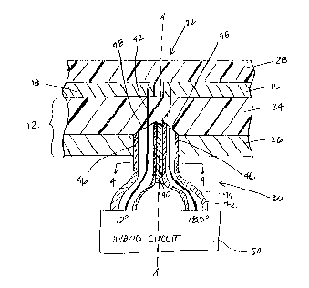
Referring to FIGS. 1-4 a dual polarization antenna 10. The antenna 10 includes
a
substrate 12 having a ground plane 26 and a dielectric layer 24 adjacent
thereto, and at least one
?o antenna unit 13 carried by the substrate. A plurality of antenna units 13
are arranged in an
array. As shown in FIG.1, the antenna 10 includes nine antenna units 13. Each
antenna unit 13
includes four adjacent antenna patches or elements 14, 16, 18, 20 axxanged in
spaced apart
xelation from one another about a central feed position 22 on the dielectric
layer 24 opposite the
ground plane 26. Preferably, diagonal pairs of antenna elements, e.g.16/18 and
14/20, define
s5 respective antenna dipoles thereby providing dual polarization as would be
appreciated by the
skilled artisan. 'Of course, only a single pair of antenna elements,
e.g.16/18, forming an antenna
.dipole may ~be provided for a.single polarization embodiment.
Each antenna unit,also includes an antenna feed structure 30 having four
coaxial feed
lines 32, 34, 36, 38 (FIG. 4). Each coaxial feed line has an inner conductor
42 and a tubular outex
2o conductor 44 in surrounding relation then eto. Referring to FIG. 2, the
outer conductors 44 have
parallel adjacent ends 46 joined together about an axis A-A and are connected
to the ground
plane 26. For example, the parallel adjacent ends 46 are joiized together via
solder 40. The ends
46 of the outer conductors 44 are tapered and arranged so that portions 48
thereof adjacent the
axis A-A extend further.beyond the ground plane 26 in the dielectric layer 24
and toward the
25 antenna elements 14,16,18, 20. The inner conductors 42 preferably extend
outwardly from the
ends 46 of respective outer conductors 44, through the dielectric layer 24 and
are connected to
respective antenna elements 14,16,18, 20 adjacent the central feed position
22.
The ends 46 of the outer conductors are symmetrically angled, and all of the
antenna
elements 14,16,18, 20 have a same shape, e.g. generally rectangular or a
generally square shape.
3o This reduces the common modes which would typically be associated with this
type of array.
The gr ound plane 26 may extend laterally outwar dly beyond a periphery of the
antenna units
13, and the.coaxial feed lines 32, 34, 36, 38 may diverge outwardly from
contact with one another
upstream from the central feed position 22 as can be seen in FIG. 2.
CA 02425950 2003-04-10
WO 02/37608 PCT/USO1/45209
The antenna 10 also include at least one hybrid circuit 50 carried by the
substrate 12 and
connected. ,to the antenna feed , structure 30. The hybrid circuit 50
controls, receives and
generates the signals to respective antenna elements 14,16, 18, 20 of the
antenna units 13 as
would be appreciated by those skilled ilz the art.
The dielectric layer has a thickness in a range of about 1/a an operating
wavelength of the
antenna 10, and at least one impedance rnatchiilg dielectric layer 28 may be
provided over the
antenna units 13. This impedance matching dielectric layer 28 may also extend
laterally
outwardly beyond a periphery of the antenna units 13 as shown in FIG. 3. The
use of the
extended substrate 12 and extended impedance matching dielectric layer 28
result in an antenna
1o bandwidth of 2:1 or greater. The subshate 12 is flexible and can be
conformally mounted to a
rigid surface; such as the nose-Bone of an aircxaft or spacecraft.
A method of making the antexuza 10 including forming the substrate 12 having a
ground
plane 26 and a dielectric layer 24 adjacent thereto, and providing at least
one antenna unit 13 on
the substrate. The antenna 10, as shown in FIG.1, includes nine antenna untis
13 arranged in
~5 an array. Providing the antenna unit 13 includes arranging four adjacent
antenna elements 14,
16,18, 20 in spaced apart relation from one another about the central feed
position 22 on the
dielectric layer 24 opposite the ground plane 26, and forming the antenna feed
structure 30
including,four coaxial feed lines 32, 34, 36, 38 each having an inner
conductor 42 and a tubular
outer conductor 44 in surrounding xelation thereto. The outer conductors 44
have parallel
zo adjacent ends 46.
Forming the antenna feed structure 30 further includes joining together the
parallel
adjacent ends 46 of the outer conductors 44 about an axis A-A, connecting the
parallel adjacent
ends of the outer conductors to the ground plane 26, tapexing and arranging
the parallel
adjacent ends of the outex conductors so that portions 48 thereof adjacent the
axis extend fuxther
25 beyond the ground plane in the dielectric layer 24 and toward the antenna
elements 14,16,18,
20, and connecting the inner conductors 42 to respective antenna elements
adjacent the central
feed position 22. The inner conductors 42 extend outwardly from the parallel
adjacent ends 46
of respective outer conductors 44. Furthermore, the parallel adjacent ends 46
of the outer
conductors.44: axe preferably joined together about an axis A-A via soldex 40.
30 The method also includes providing the at least one hybrid circuit 50 on
the substrate 12
and connected to the antenna feed structure 30. Furthermore, the method may
include providing
at least one impedance matching dielectric layex 28 to cover the antenna
uxuits 13, and which
extends laterally outwardly beyond a periphery of the at least one antenna
unit, as shown in
5
CA 02425950 2003-04-10
WO 02/37608 PCT/USO1/45209
PIG. 3.
The antenna 10 has a two to one bandwidth in the frequency range of 2-28 Ghz,
achieves
a scanarigle of ~45°, and has return loss of less than or equal to
about l0db. Thus, a lightweight
patch dipole~phased array antenna 10 with a wide frequency bandwith and a wide
scan angle
is provided. Also, the antenna 10 is flexible and can be conformally mountable
to a surface.
The dual polarization antenna includes a subshate having a ground plane and a
dielectric layer adjacent thereto, and afi least one antenna unit carried by
the substrate. The
antenna unit includes four adjacent antenna elements arranged in spaced apart
relation from
one another about a central feed position on the dielectric layer opposite the
ground plane.
1o Preferably, diagonal pairs of antenna elements define respective antenna
dipoles thereby
providing dual polarization. The antenna unit also includes an antenna feed
structure havitlg
four coaxial feed lines, each coaxial feed line including an inner conductor
and a tubular outer
conductor in surrounding relation thereto. The outer conductors have parallel
adjacent ends
joined together about an axis and are connected to the ground plane. The ends
of the outer
1s conductors are tapered and arranged so that portions thereof adjacent the
axis extend further
beyond the ground plane in the dielectric layer and toward the antenna
elements.
6