Note: Descriptions are shown in the official language in which they were submitted.
CA 02426116 2003-04-16
WO 02/33818 PCT/GBO1/04570
Frequency Synthesiser
This invention relates to a synthesiser for generating frequencies in the
range
from near zero Hertz to the millimetre and sub-millimetre wavebands. More
specifically, it relates to a synthesiser that produces an output frequency by
means of detecting laser signals using a photodetector, and is capable of
arbitrarily small frequency increments between ,the minimum and maximum
output frequency.
Background
There are many applications for frequency synthesisers that are capable of
operating over a very wide frequency range. Instrumentation, millimetre wave
and sub-millimetre wave, radar, communications systems, imaging systems,
spectroscopy applications and general laboratory test equipment have
requirements in this field. Existing ultra-wideband generators of frequencies
in the range covered by the present invention all work by switching over from
one type of frequency generator to another as the output frequency required
goes out of the range of a particular generator type.
There is one type of synthesiser that works by combining two or more laser
sources and presenting this combined signal to a photodetector. The
photodetector output will comprise, amongst other components, f~~ - f~2,
where f~~ and f~2 are the respective frequencies of the two the laser sources.
By a suitable choice of f~ and f2, any frequency can be produced that is
within
~ the bandwidth of the photodetector. There are problems with this technique.
The linewidth of a typical laser can be several megahertz (MHz) wide, and
combining two uncorrelated laser sources in a photodiode will produce an
output signal that is too noisy for most practical purposes. Techniques exist
~~
2 for ameliorating this by locking the two laser sources to a common reference
signal such as, for example, another laser source so that much of the noise is
correlated and so does not appear in the wanted output. Injection locked
lasers would commonly be used as the laser sources as these are easily
locked to a reference laser source.
CA 02426116 2003-04-16
WO 02/33818 PCT/GBO1/04570
These techniques can be used to provide an output frequency of low noise,
but they suffer the disadvantage that the system output frequency is
relatively
inflexible, in that it can only be adjusted in increments of approximately a
few
hundred MHz minimum. For instance, if a laser with multiple frequency
outputs is used as the reference source, then each of the injection locked
lasers can be locked to a different output, but when the signals are combined
in the photodetector, the output frequency step is limited to the difference
between two successive outputs from the reference laser. If the number of
frequency outputs per unit bandwidth from the reference is increased, so as
to reduce the minimum step size, then it will be harder to keep each of the
laser sources locked to one specific frequency line. Drift in the injection
locked lasers will cause them to lock on to adjacent spectral lines if the
lines
are too close to each other.
The present invention overcomes these limitations, and also provides for very
quick changes between desired frequencies. .
Statement of Invention, and Advantages
According to the present invention there is provided a radio frequency
synthesiser comprising at least one optical frequency selection and
translation
device providing a first optical output and taking an input from an optical
reference oscillator system capable of providing at least two different
optical
frequency outputs, where the first output from the selection and translation
device is combined with a second optical output signal derived from the
optical reference oscillator system and detected.
The use of a frequency translating device - a device that is capable of
providing an output frequency different from that of any of the components of
the optical reference system - along with a frequency-selection mechanism
provides for a much greater freedom in choosing the system output frequency.
There are several different types of frequency translating device that can be
used. Current methods include, but are not limited to, heterodyne optical
phase lock loops, acousto-optical frequency shifters, electro-optical
frequency
shifters, and heterodyne optical injection phase lock loops. These frequency
2
CA 02426116 2003-04-16
WO 02/33818 PCT/GBO1/04570
translating devices are able to take the input signals from the optical
reference
oscillator system operating at a particular spectral line frequency spacing,
select a desired spectral line, and produce an output signal that differs from
the selected spectral line by an amount according to the frequency of a
reference that is input to the translating device. Some of these devices take
the optical input signal,and move it in frequency, whilst others use the
optical
input signal as a basis for the generation of a new optical signal. Thus some
frequency translating devices act as tuneable sources, whilst others act
purely
as frequency shifters. The latter type will need the addition of a tuneable
optical filter if there is no filtering action inherent in its operation, to
remove
unwanted inputs from the reference oscillator system. Both types of
frequency translating device are suitable for use with the current invention.
It
will be understood that the invention is not limited to the use of the
frequency
translating devices specified above, but that any device capable of taking an
optical signal as input and providing an optical signal as output that differs
in
frequency from the input by a controlled amount may be suitable for
implementing the invention.
Note that in this specification, optical signals can be taken as being those
signals that can be generated using laser techniques. These will be of the
order 10 THz (corresponding to a wavelength of 30p) or above. Signals that
are capable of being output from a photodetector can be taken as being RF
signals. Current technology allows signals of the order 150GHz to be
detected, but the invention will work with photodetectors that have a higher
upper frequency limit.
Advantageously, the second output signal is also derived from a frequency
selecting and translating device, so that selection of an arbitrary output
frequency from the invention is more convenient, as described below.
The optical reference oscillator system will preferably be an optical
frequency
comb (OFC) generator, which is capable of generating several spectral lines
at known frequency intervals. However, it may also comprise a system of two
or more lasers locked to a common source frequency, with each laser
3
CA 02426116 2003-04-16
WO 02/33818 PCT/GBO1/04570
providing different output frequencies. In general, it can be any system that
has two or more optical output signals of different frequencies that are
capable of providing a reference to the frequency selection mechanisms.
There are various types of OFC generator, some of which will be more suited
to the current invention than others. Preferably, the spacing between adjacent
comb lines will be stable in frequency, yet adjustable to a desired frequency.
Preferably, the amplitudes of all spectral lines to be used are similar.
Preferably, all comb lines will have high phase correlation. Preferably, the
minimum comb spacing will be of the order 1 GHz to 1 OGHz, to prevent the
frequency translators from hopping from one spectral line to another.
Some possibilities are as follows:
- Mode- locked laserz:
This method employs a multi line laser who's modes are locked together by a
periodic perturbation of the laser cavity.
- Optical Parametric Oscillator Frequency Divider OFC Generator3:
This method employs a single laser to pump a set of optical parametric
oscillators, whose evenly spaced outputs form the major frequency markers of
the comb.
- External Resonant Cavity Electro-Optic OFC Generator4:
This method relies on the production of a comb of equally spaced modes from
a single carrier frequency. An electro-optic modulator is used to superimpose
a microwave frequency onto the optical carrier frequency. This produces a
comb of modes with a spacing of exactly the microwave frequency.
- Fibre methods5
There are several techniques that employ simplified optical fibre loops for
OCF generation. One of them, proposed by Ho and Kahn6 uses an electro-
optic phase modulator fibre loop structure. The basic concept here is to
place a phase modulator within a recirculating loop, so that the phase
modulation is enhanced by multiple passes of light through the modulator.
The loop also includes an optical amplifier to compensate for the round trip
loss.
Other techniques exist for OFC generation that may be suitable for use in the
current invention.
4
CA 02426116 2003-04-16
WO 02/33818 PCT/GBO1/04570
The detector will preferably be a photodiode. If a plurality of input
frequencies
are fed into a photodiode, then the square law nature of the photo-detection
process will result in the generation of difference frequency terms. Given two
optical inputs, a and b, where
a = A sin wit, and
b=Bsin~2t, .
then the detection process will result in a frequency component at ~c~~ -w2~.
This is the desired output from the frequency synthesiser system. Other,
unwanted, frequency components will also be produced, but these will tend to
be much smaller than those of the wanted term.
According to the present invention there is also provided a method of
synthesising a signal comprising the steps of:
providing a reference system having an output that has a plurality of
spectral lines within the frequency band used by a laser;
presenting this output to a frequency selection and translation device
having an output that comprises a single spectral line chosen from
those at its input that has been translated in the frequency domain by
an amount determined by a reference frequency input.
presenting the output of the reference system to a frequency selection
device that is capable of selecting a single spectral line;
taking the output from the frequency selection and translation device,
and the output from the frequency selection device, and combining and
downconverting the two outputs to produce a radio frequency signal.
Preferably, the reference system in the method described above is capable of
varying the spacing between adjacent spectral lines according to a radio
frequency reference that is placed on an input to the reference system.
5
CA 02426116 2003-04-16
WO 02/33818 PCT/GBO1/04570
Preferably, the frequency selection device in the method described above can
also incorporate frequency translation means. This gives greater versatility
in
choosing the output frequency.
The present invention can be used to generate sinusoidal waveforms. It can
also be used to generate more complex waveforms comprising of a plurality of
sinusoidal components in the RF output. Modulated RF waveforms can also
be generated in a straightforward fashion. An optical modulator can be added
in the optical path to provide modulation at optical frequencies, or the
frequency translator itself could be used to modulate its optical output.
Preferably, the modulation would be performed within the frequency
translator. More than one of the optical signals that are later combined could
be modulated, to produce a complex modulated signal.
Detailed description of the invention
The prior art, as described above, combines the outputs from two injection
locked lasers, each locked to a different spectral line from the reference
system, in the photodiode to produce the RF output frequency. To adjust the
frequency in such a device, one or both of the lasers must be locked to a
different spectral line from the reference system. The minimum frequency
step, f~, at the output of such a system is limited to the separation of the
spectral lines in the reference system, coupled with the finite ability for
the
injection locked lasers to select closely spaced spectral lines. In practice,
this
limit is of the order 1 GHz.
The current invention improves on this method. If the reference system were
able to modify its spectral line spacing, by, for example, changing the
frequency of a clock reference f~ to f~+Of~ then it becomes possible, by
changing both the particular spectral line chosen and the frequency ~f~, to
get
certain arbitrarily fine increments. The disadvantage is that the fine
increments cannot be achieved uniformly across the whole bandwidth - they
6
CA 02426116 2003-04-16
WO 02/33818 PCT/GBO1/04570
are dependent on the chosen output frequency and the number of spectral
line spacings, n, between the chosen spectral lines.
If, in this system, one of the injection locked lasers was replaced by a
frequency selecting and translating device, such that it took in as its input
a
particular spectral line, and produced as its output a signal comprising that
spectral line moved in frequency by a variable translation frequency f~, then
arbitrarily fine frequency increments are possible across the full system
bandwidth. The output of this system will be F=nf~ ~ f~. If f~ is then
incremented in steps ~f~, then F is incremented in steps ~f~, irrespective of
n
and F.
For added convenience in operation, the second injection locked laser can
also be replaced by a frequency translating device, such that it takes in as
its
input a particular spectral line, and produces as its output a signal
comprising
that spectral line moved in frequency by a translation frequency f2. The
output
of such a system will be F=nf~ ~ f~ ~ f2. If f2 is incremented in steps Of2
then F
is incremented in steps ~f2 irrespective of n and F. Furthermore, by making
~f2 a sub-multiple of Of~ interpolation between frequency increments ~f~ is
possible over the entire output frequency range.
The circuitry to produce reference signals f~, f~, f2 is relatively
straightforward,
and many techniques are commonplace in the prior art.
One system that is particularly suitable for use as a frequency translating
and
selecting device is the heterodyne optical injection phase lock loop (OIPLL).
Another system that is suitable for use as a frequency translating and
selecting device is the optical phase lock loop (OPLL).
Another system that is suitable for use as a frequency translating and
selecting device is the filtered acousto-optic or electro-optic translator.
7
CA 02426116 2003-04-16
WO 02/33818 PCT/GBO1/04570
Another system that is suitable for use as a frequency translating and
selecting device is the optical modulator. This can be an amplitude or phase
modulator, can be single or double sideband, and can use electro-optic,
acousto-optic or other physical principles to affect the input from the OFC.
For single sideband modulators a tuneable optical filter to select the
required
spectral line from the OFC can be placed at the input of the modulator. For
other modulators a tuneable optical filter must be placed at the output of the
modulator to remove unwanted outputs. Since these will be spaced from the
wanted output by the translation frequency special care must be given to
filter
selectivity to ensure adequate suppression of the unwanted output.
Advantageously, a tuneable filter can be placed at the input for all modulator
types to improve the spurious rejection of the translator. The optical
modulator is also particularly suitable for modulating the optical signal with
some desired modulation signal. This would typically be a low frequency or
baseband signal carrying some information content, but some applications
may require high frequency signals to be used as modulating waveforms.
Details on these devices are given below, and also in the appropriate
references.
The combination of the optical signals from the frequency translation devices
can be carried out either in the photodetector itself, or in a separate
combiner
and the combined optical signal carried to the photodiode by any convenient
means. It is important that the polarisation of the signals from the
translation
devices is matched before, or as they are combined. Specifically, the E-fields
of the signals should be substantially in alignment as they add vectorially.
Misalignment will lead to a less efFicient coupling, and the magnitude~of the
sum optical signal will be reduced, leading to degradation in the signal to
noise performance of the system. .
8
CA 02426116 2003-04-16
WO 02/33818 PCT/GBO1/04570
Drawings
Some examples of specific embodiments of the current invention will now be
described, by way of example only, with reference to the accompanying
illustrative drawings, in which:
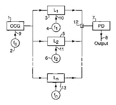
Figure 1 shows, in block diagrammatic form, the basic layout of the major
components in one form of the invention;
Figure 2 shows illustrative spectra typically present at various nodes of the
layout shown in Figure 1.
Figure 3 shows in more detail the operation of one type of frequency selecting
and translating device, the heterodyne optical phase locked loop.
Figure 4 shows in more detail the operation of another type of frequency
selecting and translating device, the optical injection phase locked loop.
Figure 5 shows in more detail the operation of another type of frequency
selecting and translating device, the filtered optical modulator.
Figure 6 shows the system also incorporating an optical modulator in one of
the outputs from the translator.
Detailed Description of the Drawings
With reference to Figure 1, an optical comb generator, OCG, 1, taking the role
of the optical reference oscillator system,.and having a frequency lock input
9,
provides a signal output comprising spectral lines spaced in frequency by the
signal frequency placed on the frequency lock-input 9. The RF frequency
reference 2 provides a signal, f~, into the frequency lock input 9, and hence
provides for spectral lines spaced at f~ on the output of the OCG.
Frequency selection and translation devices 3, 5 are each locked to one of the
spectral lines of the OCG, the choice of line depending on the desired output
9
CA 02426116 2003-04-16
WO 02/33818 PCT/GBO1/04570
frequency. Both frequency selection and translation devices 3, 5 have their
own respective RF frequency references, 4, 6.
While the frequency selection and translation devices can be operated
separately to synthesise optical frequencies locked to the OFC, RF synthesis
is achieved by combining the outputs of either two or more frequency
translation and selection devices as illustrated in Figure 1, or one frequency
translation and selection device with one or more frequency selection devices.
The following description illustrates the operation of the RF synthesisers. In
this description the frequencies cited are for illustration only; the
invention is
not restricted to these frequencies. The OFC has its reference input signal
set
to 1 GHz , the first frequency selecting and translating device, 3 has its RF
frequency reference 4 set to a frequency in the range between 1 GHz and
2GHz, in 1 MHz steps, and the second frequency translating device, 5 has its
RF frequency reference 6 set to a frequency in the range between 1GHz and
1.001 GHz, in 1 KHz steps. The lower end of the frequency spans chosen for
f~ and f2 are set much higher than theoretically required so that 1/f noise
problems are reduced and wide loop bandwidths can be used to achieve short
locking times when OPLL/OIPLL are used as the frequency translation and
selection devices.
This system is capable of providing an RF output that has a frequency range
from 1 kHz up to the upper frequency limit of the photodetector in 1 kHz
steps.
Of course, by reducing the increment size of f2, an arbitrarily small
frequency
increment, and minimum frequency, can be achieved.
The RF frequency references 2, 4, 6 each comprise of RF frequency
synthesisers, and references 4 and 6 are capable of being varied in frequency
over limited ranges mentioned above. All frequency references 2, 4, 6 are
locked to a common reference that is not shown on the diagram.
CA 02426116 2003-04-16
WO 02/33818 PCT/GBO1/04570
Further frequency selecting and translating devices, along with their
references 13 can be added to the system to produce more complex
waveforms than the sinusoids envisaged above.
Figure 2a diagrammatically illustrates a typical comb line that might be seen
at
the output of the OCG. The whole spectrum is presented to the inputs of the
frequency selection and translation devices 3, 5.
Figure 2b illustrates how the selection and translation device 3 selects a
particular component of the OCG spectrum and translates it by f~
Figure 2c illustrates how the selection and translation device 5 selects a
second component of the OCG spectrum and translates it by f2, The comb line
selected by device 5 is separated from that which is selected by device 3 by 2
f~,
Figure 2d shows that the optical spectrum presented to the optical detector as
result of combing the output of frequency selection and translation devices 3
and 5 comprises two optical components separated by 2 f~- f~+f2.
Figure 2e shows that the RF spectrum following envelop detection comprises
a single component at 2 f~- f~+ f2.
Figure 3 shows in more detail the operation of one type of frequency selecting
and translating device, the OPLL.
The input from the OFC generator 1 is combined with a sample of the output
from a tuneable slave laser 14, SL, such that their electric fields overlap,
before detection in a photo-detector 16, PD. The output from the PD 16 is
amplified in an amplifier 17, A and fed to the signal input of a mixer 18, M.
The offset frequency , fn, is applied to the local oscillator input of the
mixer 18.
The intermediate frequency output port of the mixer 18, which must have a
frequency response extending to zero frequency, is connected to the input of
11
CA 02426116 2003-04-16
WO 02/33818 PCT/GBO1/04570
a loop filter 19, LF. LF 19 is designed in accordance with well known phase-
lock loop theory to have a passband substantially less than the minimum
required offset frequency fn. LF 19 may incorporate lock acquisition and
detection circuits. The output from LF 19 is connected to the tuning control
of
SL 14. SL 14 can be a tuneable external cavity laser or preferably a
monolithic tuneable laser. The output from SL 14 forms the output from the
frequency selecting and translating mechanism. The control loop, comprising
PD 16 , A 17, M 18, LF 19, SL 14, locks when the heterodyne frequency at the
output of PD 16 is exactly equal to the offset frequency fn.
OPLLs are suitable for use where the time taken for the signal to propagate
around the control loop is small relative to the reciprocal of the spectral
linewidth of SL 14.
Figure 4 shows in more detail the operation of another type of frequency
selecting and translating device, the heterodyne OIPLL..
In this approach, a frequency translating device 20, T, which could be an
optical intensity or phase modulator or an optical single sideband modulator
using electro-optic, acousto-optic or other physical principles, is added into
the
OPLL circuit described above. It is used to translate the OFC generator's
spectrum by the required offset. The output from T 20 is coupled to the slave
laser 14 so as to injection-lock it to the required offset output frequency.
This
approach avoids the control loop delay restrictions of the OPLL and is
therefore well suited for applications where SL 14 is a monolithic
semiconductor laser. The phase lock loop path from PD through A, M and LF
to SL can be designed with a narrow bandwidth to track the environmental
disturbances on SL and so provide much wider locking ranges than could be
obtained if only injection-locking were used. The path lengths between the
offset source and T 20, and between the offset source and M are adjusted so
that the injection locking and phase locking processes add constructively.
12
CA 02426116 2003-04-16
WO 02/33818 PCT/GBO1/04570
Figure 5 shows in more detail the operation of another type of frequency
selecting and translating device, the filtered acousto-optic or electro-optic
translator.
In this approach, a frequency translating device, T, which could be an optical
intensity or phase modulator or an optical single sideband modulator using
electro-optic, acousto-optic or other physical principles, is used to
translate
the comb spectrum by the required offset. The output from T feeds a tuneable
optical filter, TF, which is tuned by a control input to select the required
offset
comb line. If non single sideband translating devices are used this approach
requires that the minimum offset frequency be large relative to the bandwidth
of the tuneable optical filter. Although not shown on the diagram, it is
advantageous to include a tuneable optical filter before the frequency
translating device T to further reduce the unwanted spurii resulting from the
mixing process. ,
Figure 6 shows an optical modulator 21 in the optical path from one of the
optical frequency translation and selection devices, which allows the system
to generate modulated signals. Typically, the modulation signal fm would be a
baseband signal, but may be an Intermediate Frequency (IF) signal that itself
comprises a carrier that has been modulated with a baseband signal.
Modulators could be positioned in the optical paths of a plurality of the
selection and translation devices to increase the versatility of the final RF
signal produced. Although the modulator is shown in Figure 6 as being
positioned before the signals are combined, it could also be positioned after
the combiner, but would then only be able to add the same modulation signal
to all optical signals
The outputs of the frequency selection and translation devices 3, 5 are
combined and applied to the photodetector. The photodetector should have a
bandwidth greater than the maximum frequency to be generated. The
combination process should be arranged so that the electric fields of the fiwo
optical outputs overlap, as discussed above.
13
CA 02426116 2003-04-16
WO 02/33818 PCT/GBO1/04570
Communications systems that incorporate the present invention will have
particular benefits. Wide band communication are possible, and frequency
changes can be made quickly. Also, signals having multiple outputs can be
produced, each having an independent modulation signal. This may be
particularly suitable for generating signals for multiple mobile receivers.
The
system will also have benefits if incorporated into radar systems, where it is
often necessary to generate wideband modulated waveforms.
An important performance parameter for any frequency synthesiser,
particularly when used in the above applications, is the level of spurious
outputs. Conventional multi-octave synthesisers frequently produce strong (> -
40 dB relative to wanted output) harmonic and sub harmonic spurious signals.
For the present invention, the level of spurious signals is determined by the
filtering effectiveness of the optical frequency selecting or optical
frequency
selecting and translating devices. Using injection locked SG-DBR lasers with
a comb line spacing of 17.5 GHz a suppression of adjacent comb lines of > 30
dB has been demonstrated', corresponding to a suppression of > 60 dB in the
detected RF output. Detailed modelling$ has shown that for an injected power
of -40 dB relative to injection locked DFB laser output power lines spaced by
10 GHz would be suppressed by > 36 dB, corresponding to a suppression of
> 72 dB in the detected RF output. Reducing the line spacing to 1 GHz would
reduce the suppression in the optical output to < 16 dB due to gain modulation
effects in the DFB laser, corresponding to a suppression of < 32 dB in the
detected RF output. For this reason and to relax injection locked DFB laser
temperature and current control requirements comb line spacings > 2 GHz are
preferable.
14
CA 02426116 2003-04-16
WO 02/33818 PCT/GBO1/04570
References:
1 "Optical Teohniques for Microwave Generation, Transmission and
Control", L Goldberg et al, 229-232, 1990 IEEE MTT-S Digest
°
2 "High Frequency Source Having Heterodyned Laser Oscillators
Injection-Locked to a Mode-Locked Laser", Granted patent, US 5,379,309
3 "Optical frequency division using an optical parametric oscillator", D Lee
and NC Wong, Optics Letters, Vo1.15 pp. 1129-1131, 1990
4 "Efficient optical frequency-comb generator", AS Bell, GM McFarlane, E
Riis, and 1 Ferguson, Optics Letters, Vol 20, No. 12, pp. 1435-1437, 1995.
5 " A multiwavelength source having precise channel spacing for WDM
systems", JJ Veselka and SK Korotky, IEEE Photonics Technology Letters,
Vol 10, no. 7 1998.
6 "Optical Frequency comb generator using phase modulation in amplified
circulating loop", KP HO and JM Kahn, IEEE Photonics Technology Letters,
Vol. 5, No. 6, p. 721-725, 1993
7 "Exact optical frequency synthesis over > 1THz using SG-DBR lasers", C. F.
C. Silva, L. N. Langley and A. J. Seeds, OLEO Europe 2000, Nice, September
2000, p. 163.
8 "Microwave frequency synthesis using injection locked laser comb line
selection", B. Cai, D. Wake and A. J. Seeds, IEEE/LEOS Summer Topical
Meeting on RF Opto-electronics, Keystone, USA, August 1995, published in
the 1995 Digest of the LEGS Summer Topical Meetings, pp. 13-14.