Note: Descriptions are shown in the official language in which they were submitted.
CA 02426422 2009-10-02
SCALEABLE INTERCONNECT STRUCTURE FOR PARALLEL COMPUTING
AND PARALLEL MEMORY ACCESS
BACKGROUND OF THE INVENTION
A persistent problem that arises in massively parallel computing systems is
supplying a sufficient flow of data to the processors. U.S. Patent No.
5,996,020 and U.S.
Patent No. 6,289,021 describe high bandwidth low latency interconnect
structures that
significantly improve data flow in. a network. What is needed is a system that
fully
exploits the high bandwidth low latency interconnect structures by supporting
parallel
memory access and computation in a network.
SUMMARY OF THE INVENTION
Multiple processors are capable of accessing the same data in parallel using
several innovative techniques. First, several remote processors can request to
read from
the same data location and the requests can be fulfilled in overlapping time
periods.
Second, several processors can access a data item located at the same
position, and can
read, write, or perform multiple operations on the same data item overlapping
times.
Third, one data packet can be multicast to several locations and a plurality
of packets can
be multicast to a plurality of sets of target locations.
In the description that follows the term "packet" refers to a uruit of data,
preferably
in serial form. Examples of packets include Internet Protocol (IP) packets,
Ethernet
frames, ATM cells, switch-fabric segments that include a portion of a larger
frame or
packet, supercomputer inter-processor messages, and other data message types
that have
an upper limit to message length.
The system disclosed herein solves similar problems in communications when
multiple packets arriving at a switch access data in the same location.
Other Multiple Level Minimum Logic Network structures can be used as a
fundamental building block in many highly useful devices and systems including
logic
devices, memory devices, and computers and processors of many types and
characteristics. Specific examples of such devices and systems include
parallel random
access memories (PRAMs) and parallel computational engines. These devices and
PAGE 11154"RCVD AT 101212009 8:21:13 PM [Eastem Daylight Time] * SVR:F0000314
* DNIS:3907 * CSID:604 682 0274' DURATION (mm.ss):17.35
CA 02426422 2009-10-02
systems include the network interconnect structure as a fundamental building
block with
embedded storage or memory and logic. Data storage can be in the form of first-
in-first-
out (FIFO) rings.
In accordance with one aspect of the invention there is provided a parallel
data
processing apparatus. The apparatus includes an interconnect structure
interconnecting a
plurality of locations and adapted to communicate information. The apparatus
also
includes at least one storage element coupled to the interconnect structure
and accessible,
as locations, via the interconnect structure. The at least one storage element
includes a
first storage element at a first location. The first storage element comprises
a plurality of
storage sections connected in paired, synchronized first-in-first-out (FIFO)
storage rings.
Each of the paired FIFO storage rings comprise a circularly-connected set of
shift
registers wherein a subset of the shift registers are shared by the rings, the
FIFO storage
rings being mutually synchronized in pairs in a configuration that
synchronously
processes data stored in the storage elements on the paired storage rings
according to an
operation determined at least in part by the communicated information. The
apparatus
also includes a plurality of computational units coupled to the interconnect
structure and
accessible as locations of the interconnect structure. The plurality of
computational units
are configured to access data from the at least one storage element, the data
synchronously circulating in the paired FIFO storage rings via the
interconnect structure.
The computational units include a first computational unit and a second
computational
unit. The first and second computational units are adapted to read from
different storage
sections of the first storage element simultaneously and send data contents of
the storage
sections of the first storage element to different target locations.
In accordance with another aspect of the invention, there is provided a
parallel
data processing apparatus. The apparatus includes an interconnect structure
interconnecting a plurality of locations and adapted to communicate
information. The
apparatus also includes a plurality of storage elements connected in paired,
synchronized
first-in-first-out (FIFO) storage rings and coupled to the interconnect
structure and
accessible, as locations, via the interconnect structure. The plurality of
storage elements
include first and second storage elements at respective first and second
locations. The
apparatus also includes a plurality of computational units coupled to the
interconnect
structure and accessible as locations of the interconnect structure, the
plurality of
computational units being configured to access data from selected ones of the
plurality of
storage elements, the data being selectively processed according to an
operation
la
PAGE 11154 RCVD AT 101212009 8:21:13 PM [Eastern Daylight TimeJ"SVR:F0000314 *
DNIS:3907 * CSID:604 682 02741 DURATION (mm.ss):17.35
CA 02426422 2009-10-02
determined at least in' part by the communicated information that
synchronously
circulates in the circularly-connected set of shift registers in each of the
paired FIFO
storage rings to enable synchronized processing of data on the paired storage
rings..
subset of the shift registers are shared by the paired FIFO storage rings. The
computational units include a first computational unit and a second
computational unit.
The first computational unit is adapted to read and operate on data from the
first and
second storage elements simultaneously. The second computational unit is
adapted to
read and operate on data from the first and second storage elements at a time
overlapping
the reading and operating of the first computational unit.
In accordance with another aspect of the invention, there is provided a
parallel
data processing apparatus. The apparatus includes an interconnect structure
interconnecting a plurality of locations and adapted to communicate
information. The
apparatus also includes a plurality of storage elements coupled to the
interconnect
structure and accessible, as locations, via the interconnect structure. The
storage elements
include a first circulating shift register, the first shift register
comprising a set of
circularly-connected bits wherein a subset of the bits is communicatively
shared. The first
shift register stores a first word having a plurality of storage sections. The
plurality of
storage elements are configured to store data that is processed according to
an operation
determined at least in part by the communicated information. The plurality of
storage
elements are connected in paired, synchronized first-in-first-out (FIFO)
storage rings
including a second circulating shift register the second shift register
comprising a set of
circularly-connected bits wherein a subset of the bits is communicatively
shared with a
subset of the bits of the first shift register. The second shift register
stores a second word
having a plurality of storage sections. The apparatus also includes a
plurality of
computational units coupled to the interconnect structure and accessible as
locations of
the interconnect structure, the plurality of computational units being
configured to operate
on separate storage sections of the first word simultaneously. The plurality
of
computational units are adapted to use information in the first word to
operate on the
second word.
In accordance with another aspect of the invention, there is provided a
parallel
data processing apparatus. The apparatus includes an interconnect structure
configured to
carry messages and including a plurality of nodes interconnected in a
hierarchy. The
-ib-
PAGE 13154"RCVD AT 101212009 8:21:13 PM Pastern Daylight Time] * SVR:F0000314
* DNIS:3907"CSID:604 682 0274E DURATION (mm.ss):17.35
CA 02426422 2009-10-02
interconnect structure includes a logic that anticipates message collisions at
a node and
resolves the message collisions according to a priority determined by the
hierarchy. The
apparatus also includes a first switch coupled to the interconnect structure
that distributes
data to the interconnect structure according to communication information
contained
within the data. The apparatus also includes a plurality of logic modules
coupled to the
interconnect structure by paired and synchronized storage rings, each of the
paired
storage rings comprising a circularly-connected set of shift registers wherein
a subset of
the shift registers are shared by the rings. Each of the plurality of logic
modules comprise
at least one storage element for storing data. The logic modules are addressed
and
activated by a message of the carried messages and adapted to process the
stored data
according to at least one of an operation determined by the message acting
upon data
contained in the message and data contained within the storage elements. The
apparatus
also includes a second switch coupled to the plurality of logic modules and
adapted to
receive data from the plurality of logic modules.
The apparatus may further include a plurality of interconnect modules coupled
to
the plurality of logic modules and coupled to the first switch, the plurality
of interconnect
modules adapted to monitor data traffic in the logic modules and control
timing of data
injection by the first switch to avoid data collisions.
The first switch may have a plurality of output ports, and the apparatus may
further include a plurality of interconnect modules coupled to the plurality
of logic
modules and coupled to the first switch. The plurality of interconnect modules
may be
respectively associated with the plurality of first switch output ports.
The plurality of logic modules may include logic that uses information
contained
within a message of the carried messages to select one of the plurality of the
logic
modules to perform an operation and select the operation to be performed.
The plurality of logic modules may have multiple different logic element types
with logic functionalities selected from among data transfer operations, logic
operations,
and arithmetic operations. The data transfer operations may include loads,
stores, reads,
and writes. The logic operations may include ands, ors, nors, nands, exclusive
ands,
exclusive ors, and bit tests, and the arithmetic operations may include adds,
subtracts,
multiplies, divides, and transcendental functions.
The apparatus may further include a plurality of interconnect modules coupled
to
the plurality of logic modules and coupled to the first switch, ones of the
plurality of
interconnect modules being adapted to monitor data traffic in the logic
modules and
-ic-
PAGE 14154 * RCVD AT 101212009 8:21:13 PM (Eastern Daylight Time) *
SVR:F0000314 z DNIS:3907 * CS1D:604 682 0274 * DURATION (mm-ss):17.35
CA 02426422 2009-10-02
include buffers and concentrators for holding and concentrating data and
controlling
timing of data injection by the first switch to avoid data collisions.
The first and second switches, the interconnect structure, and the plurality
of logic
modules may form an interconnect unit, and the apparatus may further include
at least
one computation unit coupled to the interconnect structure and positioned to
send data
outside the interconnect unit and to send data to the first switch.
The first and second switches, the interconnect structure, and the plurality
of logic
modules form an interconnect unit, and the apparatus may further include at
least one
memory unit coupled to the interconnect structure and positioned to send data
outside the
interconnect unit and to send data to the first switch.
The first switch and the second switch may handle data of multiple different
bit
lengths.
The logic modules may be dynamic processor-in-memory logic modules.
The apparatus may operate upon messages with a plurality of information and
data
fields including a payload field configured to carry a data payload, a first
address
designating a storage location holding data to be operated upon, a first
operation code
designating an operation to be executed on the data held in the first address,
a second
address designating an optional device for operating upon the data from the
first address
storage location, and a second operation code designating an operation that
the second
address device is to perform on the data from the first address storage
location.
The apparatus may operate upon messages with a plurality of information and
data
fields including a field indicating that a data packet is present, a payload
field capable of
carrying a data payload, a first address designating a storage location
holding data to be
operated upon, a first operation code designating an operation to be executed
on the data
held in the first address, a second address designating an optional device for
operating
upon the data from the first address storage location, and a second operation
code
designating an operation that the second address device is to perform on the
data from the
first address storage location.
The apparatus may further include at least one computational unit coupled to
the
second switch, the second switch being adapted to send data packets to the at
least one
computational units, the apparatus being a computational engine.
The apparatus may further include at least one storage element coupled to the
interconnect structure and accessible, as locations, via the interconnect
structure. The at
least one storage element may have a plurality of storage sections connected
in paired,
-ld-
PAGE 15154" RCVD AT 101212009 8:21:13 PM Eastern Daylight Time]
"SVR:F0000314"DNIS:3907 * CSID:604 682 0274E DURATION (mm.ss):17.35
CA 02426422 2009-10-02
synchronized first-in-fist-out (FIFO) storage rings. The apparatus may also
include a
plurality of computational units coupled to the interconnect structure and
accessible as
locations of the interconnect structure. The plurality of computational units
may be
configured to access data from the at least one storage element, the data
synchronously
circulating in the paired FIFO storage rings via the interconnect structure.
The
computational units may include a first computational unit and a second
computational
unit, the first and second computational units being adapted to read from
different storage
sections of the at least one storage element simultaneously and send data
contents of the
different storage sections to different target locations.
The apparatus may further include at least one storage element coupled to the
interconnect structure and accessible, as locations, via the interconnect
structure. The at
least one storage element may include first and second storage elements- The
apparatus
may also include a plurality of computational units coupled to the
interconnect structure
and accessible as locations of the interconnect structure. The plurality of
computational
units may be adapted to access data from the at least one storage element via
the
interconnect structure. The computational units may include a first
computational unit and
a second computational unit, the first computational unit being adapted to
read and
operate on data from the first and second storage elements simultaneously, the
second
computational unit being adapted to read and operate on data from the first
and second
storage elements at a time overlapping the reading and operating of the first
computational unit.
In accordance with another aspect of the invention, there is included a
parallel
access memory. The memory includes a plurality of logic modules connected into
a
hierarchical interconnect structure via storage rings that are mutually
synchronized in
pairs to enable synchronized processing of data stored in the logic modules
according to
operations determined at least in part by messages passing through the
interconnect
structure. Each of the paired storage rings comprise a circularly-connected
set of shift
registers wherein a subset of the shift registers are shared by the rings. The
interconnect
structure may be adapted to carry messages, anticipate message collisions at a
node, and
resolve the message collisions according to a priority determined at least
partly by the
hierarchy. The memory also includes a first switch coupled to the interconnect
structure
that distributes data to the plurality of logic modules according to
communication
information contained within the data, and a second switch coupled to the
plurality of
logic modules and receiving data from the plurality of logic modules.
- Ie-
PAGE 16154 x RCVD AT 101212009 8:21:13 PM [Eastern Daylight Time] *
SVR:FO0003141 DNIS:3907 * CSID:604 682 0274E DURATION (mm.ss):17 35
CA 02426422 2009-10-02
A logic module of the plurality of logic modules may include a communication
ring and a storage ring, the communication ring and the storage ring may be
synchronously circulating FIFOs.
A logic module of the plurality of logic modules may include a communication
ring and a storage ring, the communication ring and the storage ring being
synchronously
circulating FIFOs, an element of data being held in a single memory FIFO, the
data being
modified by the logic module as the element of data moves around the storage
ring.
A logic module of the plurality of logic modules may include a communication
ring and a storage ring, the communication ring and the storage ring may be
synchronously circulating FIFOs, an element of data being held in a single
memory FIFO,
the single memory FIFO capable of storing both program instructions and data.
A logic module of the plurality of logic modules may include a communication
ring and a storage ring, the communication ring being a mirror image of a ring
on a
bottom level of the first switch that is coupled to the communication ring.
The memory may further include a communication ring, and a plurality of
storage
rings, one or more of the logic modules of the plurality of logic modules
being associated
with the communication ring and with the plurality of storage rings.
The memory may further include a communication ring, and a plurality of
storage
.rings, at least one of the plurality of logic modules being associated with
the
communication ring and with the storage zings, the plurality of logic modules
having a
same logic element type.
The memory may further include a communication ring and a plurality of storage
rings, at least one of the plurality of logic modules being associated with
the
communication ring and with the storage rings, the plurality of logic modules
having
multiple different logic element types.
The memory may further include a communication ring and a plurality of storage
rings, at least one of the plurality of logic modules being associated with
the
communication ring and with the storage rings. The plurality of logic modules
may have
multiple different logic element types with logic functionalities selected
from among data
transfer operations, logic operations and arithmetic operations, wherein the
data transfer
operations include loads, stores, reads, and writes, the logic operations
include ands, ors,
hors, rands, exclusive ands, exclusive ors, and bit tests, and the arithmetic
operations
include adds, subtracts, multiplies, divides, and transcendental functions.
-lf-
PAGE 17154"RCVD AT 101212009 8:21:13 PM Eastern Daylight Time] * SVR:F0000314
* DNIS:39071 CSID:604 682 02741 DURATION (mm.ss):17.35
CA 02426422 2009-10-02
The memory may further include a plurality of interconnect modules coupled to
the plurality of logic modules and coupled to the first switch., The plurality
of
interconnect modules may be adapted to monitor message traffic in the logic
modules and
include buffers and concentrators for holding and concentrating messages and
controlling
timing of message injection by the first switch to avoid message collisions.
The memory
may further include a communication ring and a plurality of storage rings
circulating
synchronously with the communication ring, the storage rings storing data that
can be
accessed simultaneously from multiple sources and simultaneously sent to
multiple
destinations.
The logic modules may be dynamic processor-in-memory logic modules.
In accordance with another aspect of the invention, there is provided a
multiple-
access memory and computing device. The device includes a plurality of logic
devices,
each of the plurality of logic devices including memory devices connected in
paired,
synchronized fast-in-first-out (FIFO) storage rings. Each of the paired FIFO
storage rings
comprises a circularly-connected set of shift registers wherein a subset of
the shift
registers are shared by the rings, the FIFO storage rings being mutually
synchronized in
pairs to enable synchronized processing of data stored in the memory devices.
The device
also includes an interconnect structure coupled to the logic devices for
routing messages
and operation codes to the plurality of logic devices, the data in the memory
devices
being processed according to operations designated at least in part by the
routed
messages. The interconnect structure further includes a plurality of nodes
including
distinct first, second and third nodes, a plurality of logic elements
associated with the
plurality of nodes, and a plurality of message interconnect paths, ones of the
plurality of
message interconnect paths coupling selected nodes of the plurality of nodes
to send
messages from at least one of the plurality of nodes operating as a sending
node to at least
one of the plurality of nodes operating as a receiving node. The interconnect
structure
also includes a plurality of control signal interconnect paths, ones of the
plurality of
control signal interconnect paths coupling selected nodes of the plurality of
nodes to send
control signals from at least one node operating as a sending node to logic
elements
associated with the at least one node operating as a receiving node. The
interconnect
structure also includes a logic associated with the second node that
determines routing
decisions for the second node, a message interconnect path from the second
node
operative as a sending node to the third node operative as a receiving node
and a message
interconnect path from the first node operative as a sending node to the third
node
lg
PAGE 18154"RCVD AT 101212009 8:21:13 PM [Eastern Daylight Time] * SVR:F0000314
* DNIS:3907 * CSID:604 682 02741 DURATION (mm.ss):17.35
CA 02426422 2009-10-02
operative as a receiving node The interconnect structure also includes a
control signal
interconnect path from the first node operative as a sending node to the
logic, the control
signal enforcing a priority for sending a message from the first node to the
node over
sending a message from the second node to the third node.
In accordance with another aspect of the invention, there is provided a
multiple-
access memory and computing device- The device includes a plurality of logic
devices,
the logic devices including memory devices connected in paired, synchronized
first-in-
first-out (FIFO) storage rings. Each of the paired FIFO storage rings
comprises a
circularly-connected set of shift registers wherein a subset of the shift
registers are shared
by the rings, the FIFO storage rings being mutually synchronized in pairs to
enable
synchronized processing of data stored in the memory devices. The device also
includes
and an interconnect structure coupled to the logic devices for routing
messages and
operation codes to the logic devices, the data in the memory devices being
processed
according to operations designated at least in part by the routed messages.
The
interconnect structure further includes a plurality of nodes including
distinct first, second,
third and fourth nodes, and a plurality of interconnect paths selectively
coupling nodes of
the plurality of nodes, the interconnect paths including control interconnect
paths for
sending a control signal from a control-signal-sending node to"a logic
associated with a
control-signal-using node, and including message interconnect paths for
sending a
message from a sending node to a receiving node. The interconnect structure
also
includes the second node including message interconnect paths for sending a
message to
the third node and to the fourth node, the first node including a control
interconnect path
for sending a control signal to a logic associated with the second node, the
logic operable
so that for a first message arriving at the second node, the first node sends
a control signal
.25 to the logic, the logic using the first control signal to determine
whether to send the
message to the node or to the fourth node.
The logic may be operable so that a second message arriving at the second node
is
routed to a fifth node distinct from the second, third and fourth nodes.
In accordance with another aspect of the invention, there is provided a
multiple-
access memory and computing device. The device includes a plurality of logic
devices,
the logic devices including memory devices connected in paired, synchronized
first-in-
first-out (FIFO) storage rings. Each of the paired FIFO storage rings
comprises a
circularly-connected set of shift registers wherein a subset of the shift
registers are shared
by the rings. The FIFO storage rings being mutually synchronized in pairs to
enable
-lh-
PAGE 19154 * RCVD AT 101212009 8:21:13 PM jEastern Daylight Time] %
SVR:F000041 DNIS:3907 * CSID:604 682 02741 DURATION (mm.ss):17.35
CA 02426422 2009-10-02
synchronized processing of data stored in the memory devices. The device also
includes
an interconnect structure coupled to the logic devices for routing messages
and operation
codes to the logic devices, the data in the memory devices being processed
according to
operations designated at least in part by the routed messages. The
interconnect structure
further includes a plurality of nodes including a first node, a second node,
and a node set,
the first and second nodes being distinct nodes that are excluded from the
Dade set, the
second node being adapted to send messages to all nodes in the node set, and a
plurality
of interconnect paths selectively coupling nodes of the plurality of nodes,
the nodes being
selected in pairs including a sending node and a receiving node, the sending
node for
sending a message to the receiving node, the plurality of interconnect paths
including
message interconnect paths and control interconnect paths, the plurality of
control
interconnect paths selectively coupling nodes of the plurality of nodes as a
control-signal-
sending node for sending control signals to a logic associated with a control-
signal-using
node. The plurality of control interconnect paths include a control
interconnect path from
the first node to a logic associated with the second node, the logic uses a
control signal
from the first node to determine to which node of the node set the second node
sends a
message.
In accordance with another aspect of the invention, there is provided a
multiple-
access memory and computing device. The device includes a plurality of logic
devices,
the logic devices including memory devices connected in paired, synchronized
first-in-
first-out (FIFO) storage rings. Each of the paired FIFO storage rings
comprises a
circularly-connected set of shift registers wherein a subset of the shift
registers are shared
by the rings. The FIFO storage rings are mutually synchronized in pairs to
enable
synchronized processing of data stored in the memory devices. The device also
includes
an interconnect structure coupled to the logic devices for routing messages
and operation
codes to the logic devices, the data in the memory devices being processed
according to
operations designated at least in part by the routed messages. The
interconnect structure
further includes a plurality of nodes including a first node, a second node,
and a node set,
the first and second nodes being distinct nodes that are excluded from the
node set, the
second node being adapted to send messages to all nodes in the node set, and a
plurality
of interconnect paths selectively coupling nodes of the plurality of nodes,
the nodes being
selected in pairs including a sending node and a receiving node, the sending
node for
sending a message to the receiving node. The interconnect structure also
includes a first
logic associated with the first node adapted to determine where to route a
message from
-li-
PAGE 20154 * RCVD AT 101212009 8:21:13 PM [Eastern Daylight Time] '
SVR:F0000314 I DNIS:3907 * C$ID:604 682 02741 DURATION (mm.ss):17.35
CA 02426422 2009-10-02
the first node, and a second logic associated with the second node adapted to
determine
where to route a message from the second node, the first logic being distinct
from the
second logic, the second logic using information determined by the first logic
to
determine to which node of the node set the second node sends the message.
The second node may be adapted to send a message to a node outside of the node
set.
In accordance with another aspect of the invention, there is provided a
multiple-
access memory and computing device. The device includes a plurality of logic
devices,
the logic devices including memory devices connected in paired, synchronized
first-in-
first-out (FIFO) storage rings. Each of the paired FIFO storage rings comprise
a
circularly-connected set of shift registers wherein a subset of the shift
registers are shared
by the rings. The FIFO storage rings are mutually synchronized in pairs to
enable
synchronized processing of data stored in the memory devices. The device also
includes
an interconnect structure coupled to the logic devices for routing messages
and operation
codes to the logic devices- The interconnect structure further includes a
plurality of nodes,
each of the plurality of nodes including a plurality of input ports, a
plurality of output
ports, and a logical element that controls flow of messages through each of
the nodes, the
plurality of nodes including mutually distinct first, second, third and fourth
nodes and a
plurality of interconnect paths selectively coupling nodes of the plurality of
nodes, the
interconnect paths including control interconnect paths for sending a control
signal from a
control-signal-sending node to a logic associated with a control-signal-using
node, and
including message interconnect paths for sending messages from a message
sending node
to a message receiving node, the message interconnect paths selectively
coupling the
input ports and the output ports, the plurality of control interconnect paths
coupling
nodes and logical elements for sending control signals from a control-signal-
sending node
to a. logical element associated with a node having a message flow that
depends on the
control signals. The interconnect structure also includes the second node
being associated
with a logical element that uses a plurality of control signals from the first
node to
determine routing of a first message passing through the second node, wherein
the
plurality of control signals include a first control signal received from the
first node
causing sending of the first message to the third node, and a second control
signal
received from the first node causing sending of the first message from the
second node to
the fourth node.
Ij
PAGE 21154"RCVD AT 101212009 8:21:13 PM [Eastern Daylight Time] I SVR:F0000314
* DNIS:3907 * CSID:604 682 0274"DURATION (mm.ss):17.35
CA 02426422 2009-10-02
The routing of a second message passing through the second node may be the
same whether the control signal from the first node is the first control
signal or the second
control signal.
The control signal sent to the second node may be tapped from a an output port
of
the first node.
In accordance with another aspect of the invention, there is provided a
multiple-
access memory and computing device. The device includes a plurality of logic
devices,
the logic devices including memory devices connected in paired, synchronized
first-in-
first-out (FIFO) storage rings. Each of the paired FIFO storage rings comprise
a
circularly-connected set of shift registers wherein a subset of the shift
registers are shared
by the rings. The FIFO storage rings are mutually synchronized in pairs to
enable
synchronized processing of data stored in the memory devices. The device also
includes
an interconnect structure coupled to the logic devices for routing messages
and operation
codes to the logic devices, the data in the memory devices being processed
according to
operations designated at least in part by the routed messages. The
interconnect structure
further includes a plurality of nodes including a first node and a node set,
the node set
including a plurality of nodes that are adapted to send messages to the fiRst
node, and a
plurality of interconnect paths selectively coupling nodes of the plurality of
nodes, the
interconnect paths including message interconnect paths for sending a message
from a
sending node to a receiving node, the nodes in the node set having a priority
relationship
for sending a message to the first node in, which the node having a highest
priority for
sending the message to the first node is never blocked from sending the
message to the
first node.
The node set may include second and third nodes, the second node may by able
to
send a message to the first node independent of a message sent to the first
node from the
third node of the node set having a priority lower than the second node of the
node set for
sending the message to the first node.
The priority relationship among the nodes in the node set may be adapted to
send
a message to the first node depends on the position of the individual nodes in
the node set
within the interconnect structure.
In accordance with another aspect of the invention, there is provided a
computing
apparatus for usage in a computing system. The apparatus includes first and
second
synchronized first-in-first-out (FIFO) rings. Each of the FIFO rings comprise
a circularly-
connected set of shift registers wherein a subset of the shift registers are
shared by the
-lk-
PAGE 22154"RCVD AT 101212009 8:21:13 PM f Eastem Daylight
Time]"SVR:F0000314"DNIS:3901"CSID:604 682 0274 *DURATION (mm.ss):11.35
CA 02426422 2003-04-22
WO 02/33565 PCT/USO1/50543
BRIEF DESCRIPTION OF THE DRAWINGS
The features of the described embodiments believed to be novel are
specifically set
forth in the appended claims. However, embodiments of the invention relating
to both structure
and method of operation, may best be understood by referring to the following
description and
accompanying drawings.
FIGURE 1 is a schematic block diagram showing an example of a generic system
constructed from building blocks including a plurality of network interconnect
structures.
FIGURE 2 is a schematic block diagram illustrating a parallel memory structure
such
as a parallel random access memory (PRAM) that is constructed using network
interconnect
structures as fundamental elements.
FIGURE 3 is a diagram of the bottom level of the top switch showing
connections to a
communication ring, a plurality of logic modules, a circulating FIFO data
storage ring, and
connections to the top level of the bottom switch.
FIGUREs 4A, 4B and 4C are block diagrams that depict movement of data through
the
communication ring and the circulating FIFO data storage ring. FIGURE 4A
applies to both
READ and WRITE requests. FIGUREs 4B and 4C apply to a READ request in
progress.
FIGURE 5 illustrates a portion of the interconnect structure while executing
two read
operations, reading from the same circulating data storage ring occurring at
overlapping time
intervals and entering a second switch where the read data are directed to
different targets.
FIGURE 6 illustrates a portion of the interconnect structure while executing a
WRITE
instruction.
FIGURE 7 is a schematic block diagram that illustrates a structure and
technique for
performing a multicast operation using indirect addressing.
DETAILED DESCRIPTION
Referring to FIGURE 1, a schematic block diagram illustrates an example of a
generic
system 100 constructed from building blocks including one or more network
interconnect
structures. In the illustrative example, the generic system 100 includes a top
switch 110 and a
bottom switch 112 that are formed from network interconnect structures. The
term "network
interconnect structure" may refer to other interconnect structures. Other
systems may include
additional elements that are formed from network interconnect structures. The
generic system
100 depicts various components that may be included as core elements of a
basic exemplary
-2-
CA 02426422 2003-04-22
WO 02/33565 PCT/USO1/50543
system. Some embodiments include other elements in addition to the core
elements. Other
elements may be included such as: 1) shared memory, 2) direct connections 130
between the
top switch and the bottom switch; 3) direct connections 140 between bottom
switch and the 1/0,
and 4) a concentrator connected between the logic units 114 and the bottom
switch 112.
The generic system 100 has a top switch 110 that functions as an input
terminal for
receiving input data packets from input lines 136 or buses 130 from external
sources and
possibly from the bottom switch, and distributing the packets to dynamic
processor-in-memory
logic modules (DPIM) 114. The top switch 110 routes packets within the generic
system 100
according to communication information contained within the packet headers.
The packets are
sent from the top switch 110 to the DPIM modules 114. Control signals from the
DPIM
modules 114 to the top switch 110 controls timing of packet injection to avoid
collisions.
Collisions that could otherwise occur with data in the DPIMs or with data in
the bottom switch
are prevented. The system may pass information to additional computational,
communication,
storage, and other elements (not shown) using output lines and buses 130, 132,
134 and 136.
Data packets enter the top switch 110 and proceed to the target DPIMs 114
based on an
address field in each packet. Information contained in a packet may be used,
possibly in
combination with other information, to determine the operation performed by
the logic DPIMs
114 with respect to data contained in the packet and in the DPIM memory. For
example,
information in the packet may modify data stored in a DPIM memory, cause
information
contained within the DPIM memory to be sent through the bottom switch 112, or
cause other
data generated by a DPIM logic module to exit from the bottom switch. Packets
from the
DPIM are passed to the bottom switch. Another option in the generic system 100
is the
inclusion of computation units, memory units, or both. Computational units 126
can be
positioned to send data packets through 1/0 unit 124 outside system 100, or to
the top switch
110, or both. In the case of the bottom switch sending a packet to the top
switch, the packet can
be sent directly, or can be sent through one or more interconnect modules (not
shown) that
handle timing and control between integrated circuits that are subcomponents
of system 100.
Data storage in one example of the system has the form of first-in-first-out
(FIFO) data
storage rings R in DPIM 114, and conventional data storage associated with
computation units
(CUs) 126. A FIFO ring is a circularly-connected set of single-bit shift
registers. A FIFO ring
includes two kinds of components. In a first example that is conventional, the
FIFO ring
includes single-bit shift registers that are connected only to the next single-
bit shift register to
form a simple FIFO 310. In a second example, other shift registers of the ring
are single-bit or
multiple-bit registers contained within other elements of the system, such as
logic modules 114.
Taken together, both kinds of components are serially connected to form a
ring. As an example,
-3-
CA 02426422 2003-04-22
WO 02/33565 PCT/USO1/50543
the total length FL of a FIFO ring can be 200 bits with 64 bits stored in a
plurality of logic
modules L and the remaining 136 bits stored in serially connected registers of
the FIFO. A
system-wide clock is connected to the FIFO elements and shift registers and
causes data bits to
advance to the next position in a "bucket-brigade" fashion. A cycle period is
defined to be the
time in clock periods for data to complete precisely one cycle of a FIFO ring.
The integer value
of the cycle period is the same as the length in components of the FIFO ring.
For example, for
a ring of 200 components (length 200), the cycle period is 200 system clock
periods. The
system may also include local timing sources or clocks that step at a
different rate. In some
embodiments, all FIFO rings in the system have the same length, or vary at
integer multiples of
a predetermined minimum length. In alternative embodiments, a ring is a bus
structure with a
plurality of parallel paths with the amount of data held in the ring being an
integer multiple of
the ring length FL.
In the generic system 100, a top switch is capable of handling packets having
various
lengths up to a system maximum length. In some applications, the packets may
all have the
same length. More commonly, packets having different lengths may be input to
the top switch.
The length of a given packet is PL, where PL is not larger than FL.
Similarly, the bottom switch can handle packets of various lengths. Typical
embodiments of the generic system 100 generate data having different bit
lengths according to
the functions and operation of the DPIM logic modules 114 and CUs 126. The
DPIMs can
function independently or there can be a plurality of systems, not shown, that
gather data from
the DPIMs and may issue data to the DPIMs or to other elements contained
inside or outside of
system 100.
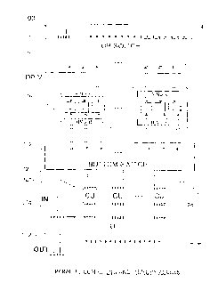
Referring to FIGURE 2, a schematic block diagram illustrates an example of a
parallel
random access memory (PRAM) system 200 constructed from fewer building blocks
than were
included in FIGURE 1. The PRAM system includes a top switch 110, a
concentrator 150, and a
bottom switch 112, which are formed from network interconnect structures. The
system also
includes DPIMs 114 that store data. The DPIM units are typically capable of
performing READ
and WRITE functions, thus the system can be used as a parallel random access
memory.
In an illustrative embodiment, a data packet entering the top switch 110 has a
form as
follows:
Payload I Operation Code 2 Address 2 1 Operation Code I I Address I I Timing
BIT,
-4-
CA 02426422 2003-04-22
WO 02/33565 PCT/US01/50543
Abbreviated as:
PAYLOAD I OP2 I AD2 I OP1 I ADI I BIT.
The number of bits in the PAYLOAD field is designated PayL. The number of bits
in
OP2 and OP1 are designated OP2L and OP I L, respectively. The number of bits
in AD2 and
ADI are designated AD2L and AD1L, respectively. The BIT field is a single bit
in length in
preferred embodiments.
The following table is a brief description of the packet fields.
Field Description
BIT Value `1' indicates that a packet is present, value `0' indicates that no
packet is present.
ADI Address used by the top switch 110 to route the packet to the target
DPIMADI 114.
OP1 Operation code used by the target DPIM 114, which specifies what
action or process the DPIM performs with the objects of the action or
process being the Payload field and the contents of the data stored in
one or more storage rings R located in the target DPIM.
AD2 Address used by the bottom switch 112 to route DPIM output to an
external device through output links 132 or to a computational unit
126. In some operations, the AD2 field is not used. If used, the AD2
field includes a leading BIT2 field that is set to 'U.
OP2 Operation code used by the computational unit 126 or the external
device located at the output port of the bottom switch 124 having
address AD2. In some operations, the OP2 field is not used.
PAYLOAD The data contents or "payload" of the packet that is routed by top
switch 110 to the target DPIM 114 at address AD1. In some
operations, the PAYLOAD field can be altered by DPIM 114 and
further transmitted by bottom switch 112 to the output port specified
by AD2. In some operations, the payload field is not used.
The BIT field enters the switch first, and is always set to I to indicate that
a packet is
present. The BIT field is also described as a "traffic bit". The ADI field is
used to route the
packet through the top switch to the packet's target DPIM. The top switch 110
can be arranged
in a plurality of hierarchical levels and columns with packets passing through
the levels. Each
time the packet enters a new level of the top switch 110, one bit of the AD1
field is removed
and the field is thereby shortened. System 200 uses the same technique. When
the packet exits
the top switch 110, no AD 1 field bits remain. Thus, the packet leaves the top
switch having the
form, as follows:
-5-
CA 02426422 2003-04-22
WO 02/33565 PCT/US01/50543
PAYLOAD I OP2 I AD2 I OP 1 I BIT.
The systems 100 and 200 include DPIM units. FIGURE 3 is a schematic block
diagram illustrating an example of a DPIM unit 114 and showing data and
control connection
paths between the DPIM and top 110 and bottom 112 switches. FIGURE 3
illustrates four data
interconnect structures Z, C, R and B. Interconnect structure Z can be a FIFO
ring located in the
top switch 110. The interconnect structures C and R are FIFO rings located in
the DPIM
module. In some embodiments, the DPIMs send data directly to the bottom
switch. In those
embodiments, if the bottom switch is an interconnect structure, then
interconnect structure B is
a FIFO ring. In other embodiments, the DPIMs send data to a concentrator that
then sends data
to the bottom switch. In those embodiments, if the concentrator is an
interconnect structure,
then B is a data FIFO that may or may not be a ring. FIGURES 1 and 7
illustrate systems that
do not include concentrators. FIGURES 2, 3, 4A and 5 illustrate systems that
contain
concentrators.
Data travels through the top switch 110 and arrives at a target output ring Z,
where J =
ADI . The ring Z = Zj has a plurality of nodes 330 connected to output lines
326. The DPIM
module includes a packet-receiving ring C 302 referred to as a "data
communication ring" and
one or more "data storage rings" R 304. FIGURE 3 illustrates a DPIM with a
single data
storage ring R. Each of the structures Z, C, R and B are FIFOs that include
interconnected
single bit FIFO nodes. Some of the nodes in the structure have a single data
input port and a
single data output port and are interconnected to form a simple multi-node
FIFO. Other nodes
in the structures have an additional data input port, an additional data
output port, or both. The
nodes may also contain control signal output ports or control signal input
ports. Ring Z
receives control signals from Ring C and sends data to logic modules L 314.
Rings C and R
receive and send data to the logic modules L 314. FIFO B 380 sends control
signals to the
logic modules L and receives data from the logic modules L. A DPIM can contain
multiple
logic modules capable of sending data to multiple input ports in interconnect
structure or FIFO
B. Data from a DPIM can be injected into multiple rows into the top level of
the system B.
The number of DPIMs may be the same as the number of memory locations, where
each DPIM
has a single storage ring R that contains one word of data. Alternatively, a
DPIM unit may
contain a plurality of storage rings R. A particular storage ring can be
identified by a portion of
the address ADI field or by a portion of the operation OPI field.
The timing of packet movement is synchronized in all four rings. As packets
circulate
in the rings, the packets are aligned with respect to the BIT field. As an
advantageous
consequence of the alignment, ring C sends control signal 328 to ring Z that
either permits or
prevents a node in Z from sending a packet to C. Upon receiving permission
from a node 330
-6-
CA 02426422 2003-04-22
WO 02/33565 PCT/US01/50543
on ring C, a node 312 on ring Z can send a packet to logic module L such that
logic module L is
positioned to process the packet immediately in bit-serial manner. Similarly,
packets
circulating in data storage ring R are synchronized with ring C so that the
logic module L can
advantageously process respective bits as packets circulate in the respective
rings. The data
storage rings R function as memory elements that can be used in several novel
applications that
are described hereinafter. A separate data communication ring (not shown)
between nodes of
ring Z and logic modules L can be used for inter-chip timing and control where
the DPIMs are
not on the same chip as the top switch.
Data in a storage ring R may be accessed from the top switch 110 by a
plurality of
packets, aligned and overlapping with portions of the packets in the Z ring
306 of the top
switch, and coinciding in cycle period. A plurality of logic modules 314 are
associated with the
data communication ring C and data storage ring R. A logic module L is capable
of reading
data from rings C and R, performing operations on the data under some
conditions, and writing
to rings C and R. The logic module L is further capable of sending a packet to
a node 320 on
FIFO 308 at the bottom switch 112 or concentrator. A separate data
communication ring (not
shown) between the logic modules L 314 and the nodes 320 of interconnect
structure B may
used for inter-chip timing and control in instances that the DPIMs are not on
the same chip as
the bottom switch. A separate data communication ring can also be used for
timing and control
operations when a single device needs to access several bits of the
communication ring in a
single cycle period.
Packets enter communication ring C through the logic modules 314. Packets exit
the
logic modules L and enter the bottom switch through input channels at
different angles.
In some examples of the generic system 100, all of the logic modules along
rings C and
R of a DPIM 114 are the same type and perform a similar logic function. Other
examples use a
plurality of different logic module types, permitting multiple logical
functions to operate upon
data stored in ring R of a particular DPIM. As data circulates around ring R,
the logic modules
L 314 can modify the data. A logic module operates on data bits passing
serially through the
module from ring C and ring R, and from a node on ring Z. Typical logic
functions include (1)
data transfer operations such as loads, stores, reads, and writes; (2) logic
operations such as
AND, OR, NOR, NAND, EXCLUSIVE OR, bit tests, and the like; and (3) arithmetic
operations such as adds, subtracts, multiplies, divides, transcendental
functions, and the like.
Many other types of logic operations may be included. Logic module
functionality can be
hardwired into the logic module or functionality can be based on software that
is loaded into the
logic modules from packets sent to the logic module. In some embodiments, the
logic modules
associated with a particular data storage ring R act independently. In other
embodiments, logic
-7-
CA 02426422 2003-04-22
WO 02/33565 PCT/USO1/50543
module groups are controlled by a separate system (not shown) that can receive
data from a
group of logic modules. In still other embodiments, the logic module groups
are controlled by a
logic module control system. In still other embodiments, the logic module
control systems
perform control instructions on data received from the logic modules.
In FIGUREs 1 and 2, each DPIM includes one ring R and one ring C. In alternate
embodiments of system 100, a particular DPIM 114 includes multiple R rings. In
multiple R
ring embodiments, a logic module 314 can simultaneously access data from the C
ring and all
of the R rings. Simultaneous access allows a logic module to modify the data
on one or more of
the R rings based on the content of R rings and also based on the content of
the received packet
and associated communication ring C.
A typical function performed by the logic modules is execution of an operation
designated in the OP1 field that operates on data held in the PAYLOAD field of
the packet in
combination with data held in the ring R. In one specific example, operation
OPI may specify
that data in the PAYLOAD field of the packet be added to data contained in
ring R located at
address ADI. The resulting sum is sent to the target port of the bottom switch
at address AD2.
As specified by the instruction held in the data field of the OP1 operation,
the logic module can
perform several operations. For example, the logic module can leave data in
ring R 304
unchanged. The logic module can replace data in ring R 304 with contents of
the PAYLOAD
field. Alternatively, logic module L can replace data held in the PAYLOAD
field with the
result of a function operating on contents previously within ring R 304 and
the PAYLOAD
field. In other examples, a memory FIFO can store program instructions as well
as data.
A generic system 100 that includes more than one type of logic module 314
associated
with a communication ring C and a storage ring R may use one or more bits of
the OPI field to
designate a specific logic module that is used in performing an operation. In
some
embodiments multiple logic modules perform operations on the same data. The
set of logic
modules at address ADI = x may perform different operations than the set of
logic modules at
address ADI = y.
Efficient movement of data packets through the generic system 100 depends on
timing
of the data flow. In some systems, buffers (not shown) associated with the
logic module help
maintain timing of data transfer. In many embodiments, timing is maintained
without buffering
data. The interconnected structure of the generic system 100 advantageously
has operational
timing that results in efficient parallel computation, generation, and access
of data.
A generic system 100 composed of multiple components including at least one
switch,
a collection of data storage rings 304, and associated logic modules 314 can
be used to
-8-
CA 02426422 2003-04-22
WO 02/33565 PCT/USO1/50543
construct various computing and communication switches. Examples of computing
and
communication switches include an IP packet router or switch used in an
Internet switching
system, a special purpose sorting engine, a general-purpose computer, or many
parallel
computational systems having general purpose or specific function.
Referring to FIGURE 2, a schematic block diagram illustrates a parallel random-
access
memory (PRAM) that is constructed using network interconnect structures as
fundamental
elements. The PRAM stores data that can be accessed simultaneously from
multiple sources and
simultaneously sent to multiple destinations. The PRAM has a top switch 110
and may or may
not have communication rings that receive packets from the target ring of the
top switch 110.
In interconnect structures that have no communication ring, the ring Z passes
through the logic
modules. The top switch 110 has T output ports 210 from each of the target
rings. In a typical
PRAM system 200, the number of address locations will be greater than the
number of system
I/O ports. As an example, a PRAM system may have 128 VO ports that access 64K
words of
data stored in DPIMs. The ADI field is 16 bits long to accommodate 64K DPIM
addresses
114. The AD2 field is 8 bits long to accommodate the 128 output ports 204,
where 7 bits hold
the address, and 1 bit is the BIT2 portion of the address. The top switch has
128 input ports
202, and 64K Z rings (not shown) each with multiple connections to a DPIM unit
via output
ports 206. Concentrator 150 has 64K (65,536) input ports 208 and 128 output
ports 210. The
bottom switch 112 has 128 input ports and 128 output ports 204. The
concentrator follows the
same control timing and signaling rules for input and output as the top and
bottom switches and
the logic modules.
Alternatively, a top switch may have fewer output Z rings and associated DPIM
units.
The DPIM units can contain multiple R rings so that the same total data size
remains
unchanged.
The illustrated PRAM shown in FIGURE 2 includes DPIM units 114 containing
logic
modules 314 that connect directly to communication ring C 302 and storage ring
R 304. DPIM
units 114 connect to packet concentrator 150 that feeds output data into
bottom switch 112.
Referring to FIGURE 3, nodes 330 on ring C send control signals to nodes 312
on ring
Z of the top switch, permitting individual nodes 312 of the ring Z to send a
packet to the logic
modules L. When a logic module L receives the packet from the ring Z, logic
module L may
perform one of several actions. First, the logic module L can begin placing
the packet on the C
ring. Second, the logic module L can begin to use the data in the packet
immediately. Third,
logic module L can immediately begin to send a generated packet into
concentrator 150 without
placing the packet on the C ring. A logic module Li can begin to place a
packet P on the C ring.
After the logic module Li has placed several bits on the ring, another logic
module Lk, where k
-9-
CA 02426422 2003-04-22
WO 02/33565 PCT/USO1/50543
> i, may begin processing and removing the bits. In some cases, the entire
packet P is never
placed on the ring C. Logic modules can insert data to either the C ring or
the R ring, or can
send data to the concentrator 150. Control of a packet entering the
concentrator is aided by
control signals on line 324 from the concentrator. Logic modules 314
associated with a ring R
304 may include additional send and receive interconnections to an auxiliary
device (not
shown) that can be associated with the ring R. The auxiliary device can have
various structures
and perform various functions depending on the purpose and functionality of
the system. One
example of an auxiliary device is a system controller.
In some embodiments, PRAM 200 has DPIMs containing logic modules 314 that all
have the same logic type and perform the same function.
In other embodiments, a first DPIM S at a particular address may have logic
modules of
different type and function. A second DPIM T may have a logic modules of the
same or
different types in comparison to the first DPIM S. In an example of PRAM
application, one
data word is stored in a single storage ring R. As data circulates in ring R,
the logic modules
may modify the data. In the PRAM, the logic modules alter the contents of the
storage ring R,
which may store program instructions as well as data.
The PRAM stores and retrieves data using packets defined to include fields,
defined as
follows:
PAYLOAD IOP2I AD2I OP1 I AD1 OBIT.
The BIT field set to I to indicate that a packet is present enters the generic
system 100.
The AD I field designates the address of a specific DPIM, which includes a
data storage ring R
304 containing the desired data. The top switch routes the packet to a
DPIM(ADI) specified by
address AD I. In the illustrative example, the OP1 field is a single bit that
designates the
operation to be executed. For example, a logic value I specifies a READ
request and a logic
value 0 specifies a WRITE request.
In a READ request, the receiving logic module in the DPIM at location AD1
sends data
stored on ring R to address AD2 of the bottom switch 112. In a WRITE request,
the PAYLOAD
field of the packet is placed on the ring R at address AD 1. AD2 is an address
designation that is
used to route data through the bottom switch 112 only in a READ request and
specifies the
location to which the content of the memory is sent. OP2 optionally describes
the operation that
a device at address AD2 is to perform on the data sent to the AD2 device. If
operation OP I is a
READ request, the logic module that executes the READ operation does not use
the
PAYLOAD field.
-10-
CA 02426422 2009-10-02
rings. The FIFO rings are adapted to communicate messages and mutually
synchronized
in pairs to enable synchronized processing of data stored on the paired
storage rings
according to operations determined at least in part by the communicated
messages. The
apparatus also includes at least one logic module coupled to the first and
second
synchronized FIFO rings and adapted to access at least one bit of each FIFO
ring
simultaneously.
The computing apparatus may further include a connection to a computer system-
wide clock, ones of the first and second FIFO rings including a plurality of
bits that
advance to a next position in a bucket-brigade manner, a cycle period of the
clock being
defined to be a time in clock periods for the plurality of bits to complete
precisely one
cycle of the ones of the first and second FIFO rings.
The computing apparatus may further include at least one synchronized (FIFO)
ring in addition to the first and second FIFO rings, the at least one logic
module being
capable of simultaneously accessing data from the first FIFO ring and the
second FIFO
ring and the at least one synchronized FIFO ring.
The at least one logic module may be positioned to read two bits of each of
the
first and second FIFO rings in a single clock period.
The at least one logic module upon receiving a message packet may be adapted
to
perform at least one action selected from among transferring the message
packet to
another FIFO ring, using information in the packet, and immediately
transmitting the
message packet outside the apparatus.
The at least one logic module may be capable of accessing multiple bits of the
FIFO rings at one time.
30
-ii-
PAGE 23154"RCVD AT 101212009 8:21:13 PM (Eastern Daylight Time] *
SVR:F00003141 DNIS:3907 * CSID:604 682 0274 DURATION (mm.ss):17.35
CA 02426422 2003-04-22
WO 02/33565 PCT/USO1/50543
copied into the payload section of the packet. In the case of a WRITE request,
the data in the
payload section of the packet can be transferred from the packet to storage
ring R.
READ Request
In a READ request, a packet P has the form:
PAYLOAD I OP2 J AD2 I OP1 J ADl JBIT.
The packet is entered into the top switch. In general, a logic module of the
DPIM at
address AD 1 identifies a READ request by examining the operation code OP I
field. The logic
module replaces the PAYLOAD field of the packet with the DATA field from ring
R. The
updated packet is then sent through the concentrator into the bottom switch
that directs the
packet to a computation unit (CU) 126 or other device at address AD2. The CU
or other device
can execute the instruction designated by operation code 2 (OP2) in
conjunction with data in the
PAYLOAD field.
The packet P enters a node T 312 on ring Z. Node T, in response to the timing
bit of
packet P entering node T and to a non-blocking control signal from a node 330
on ring C,
begins to send packet P down a data path 326 to a logic module L. When the BIT
and OPI
fields have entered logic module L, a control signal on line 324 also has
arrived at logic module
L, indicating whether the concentrator 150, or bottom switch if the structure
includes no
concentrator, can accept a message. If the control signal indicates that the
concentrator cannot
accept a message, then logic module L begins transferring packet P to ring C.
Packet P moves
to the next logic module on ring C.
At some point, one of the logic modules L on ring C receives a not busy
control signal
from below in the hierarchy. At that time logic module L begins transferring
the packet P to an
input node 320 on interconnect structure B.
In a READ request, the logic module strips the OPI field from the packet and
begins
sending the packet on path 322 to an input node 320 of the concentrator.
First, the logic module
sends the BIT field, followed by the AD2 field, followed by the OP2 field.
Timing is set so that
the last bit of the OP2 field leaves the logic module at the same time that
the first bit of the
DATA field on storage ring R arrives at the logic module. The logic module
leaves the DATA
field in storage ring R unchanged, puts a copy of DATA in the PAYLOAD field of
the packet
sent downward, and continues sending the packet in a bit-serial manner into
the concentrator.
Data in ring R remains unchanged.
-12-
CA 02426422 2003-04-22
WO 02/33565 PCT/USO1/50543
The packet enters and leaves the concentrator unchanged, and enters bottom
switch 112
having the form:
DATA I OP2 I AD2 BIT.
The PAYLOAD field now contains the DATA field from ring R. As the packet is
routed through the bottom switch, the AD2 field is removed. The packet exits
output port 204 at
address AD2 of the bottom switch. Upon exit, the packet has the form:
DATA I OP2 I BIT.
The OP2 field is a code that can be used in a variety of ways. One use is to
indicate the
operation that a bottom-switch output device performs with the data contained
in the
PAYLOAD field.
The interconnected structures of the PRAM inherently have a circular timing
that
results in efficient, parallel generation and access of data. For example, a
plurality of external
resources at different input ports 202 may request READ operations for the
same DATA field at
a particular DPIM 114. A plurality of READ requests can enter a particular
target ring Z 306 of
the top switch at different nodes 312, and subsequently enter different logic
modules L of the
target DPIM. The READ requests can enter different logic modules on ring C
during the same
cycle period. Communication ring C 320 and memory ring R 304 are always
synchronized with
regard to the movement of packets in the target ring Z of the top switch, and
input interconnect
structure B of the concentrator.
A READ request always arrives at a logic module at the correct time for the
data from
ring R to be appended in the proper PAYLOAD location of the forwarded packet.
The
advantageous result is that multiple requests for the same data in ring R can
be issued at the
same time. The same DATA field is accessed by a plurality of requests. The
data from ring R is
sent to multiple final destinations. The plurality of READ operations execute
in parallel and the
forwarded packets reach a plurality of output ports 204 at the same time. The
multiple READ
requests are executed in overlapping manner by simultaneously reading from
different locations
in ring R by different logic modules. Moreover, other multiple READ requests
are executed in
the same cycle period at different addresses of the PRAM memory.
The READ requests are executed in an overlapped, efficient and parallel manner
because of the system timing. FIGUREs 4A, 4B, and 4C illustrate timing for a
single READ.
Storage ring R is the same length as the communication ring C. Ring R contains
circulating
data 414 of length PayL. Remaining storage elements in ring R contain zeroes,
or "blanks," or
-13-
CA 02426422 2003-04-22
WO 02/33565 PCT/USO1/50543
are ignored and can have any value. The BLANK field 412 is the set of bits
that are not
contained in the DATA field 414.
Referring to FIGURE 4A, portions of each ring C and R pass through logic
modules of
a particular DPIM. A logic module contains at least two bits of the set of
shift registers
constituting ring C, and at least two bits of the shift registers constituting
ring R. In some
embodiments, the DPIM 314 contains a plurality of logic modules 314. A logic
module is
positioned to read two bits of the communication ring 302 in a single clock
period. At a time
indicated by a global signal (not shown), the logic module examines the BIT
field and the OPI
field. In the illustrated embodiment, the logic module reads the entire ON
field and the BIT
field together. In other embodiments, the OP1 and BIT fields may be read in
multiple
operations. In a READ request, an unblocked logic module 314 sends the packet
into the
concentrator or bottom switch at the correct time to align the packet with
other bits in the input
of the concentrator or bottom switch.
In a READ request, a blocked logic module places the packet on ring C where
the
packet will move to the next logic module. The next logic module may be
blocked or
unblocked. If a subsequent logic module is blocked, the blocked logic module
similarly sends
packet on ring C to the next module. If the packet enters the right-most logic
module LR that is
blocked, then logic module LR sends the packet through the FIFO on ring C.
Upon exiting the
FIFO the packet enters the left-most logic module. The packet circulates until
the packet
encounters a logic module that is unblocked. The length of ring C is set so
that a circulating
packet always fits completely on the ring. Alternatively stated, the packet
length, PL, is never
greater than the ring length, FL.
In a READ operation, a packet has the form:
PAYLOAD I OP2 I AD2 I OP1 I ADI I BIT
The packet is inserted into the top switch. Address field ADI indicates the
target
address of the ring R 304 that contains the desired data. Operation field OP 1
indicates a READ
request. Address field AD2 is the target address of the output port 204 of the
bottom switch
where the result are sent. Operation code OP2 designates a function to be
performed by the
output device.
In a typical embodiment, the output device is the same as the input device.
Thus a
single device is connected to an input 202 and output 204 port of the PRAM.
For a READ
request, the PAYLOAD field is ignored by the logic module and may have any
value. In
contrast, in a WRITE operation the PAYLOAD field contains data to be placed on
ring R 304
-14-
CA 02426422 2003-04-22
WO 02/33565 PCT/USO1/50543
associated with the DPIM at address AD1. The altered packet leaving the logic
module has the
form:
I DATA I OP2 I AD2 I BIT
Data entering the bottom switch has the form:
I DATA I OP2 I BIT I.
Data leaves the bottom switch through the output port designated by address
field AD2,
where DATA is the data field 414 of ring R.
FIGUREs 4A, 4B, and 4C illustrate timing coordination between communication
ring
C, data storage ring R, and the concentrator B. In an embodiment with rings
containing a
plurality of parallel FIFOs in a bus arrangement, a logic module 314 is
capable of reading
multiple bits at one time. In the present example, logic module L receives
only one bit per
clock period. The concentrator B includes a plurality of input nodes 320 on a
FIFO 308 that
can accept a packet from a logic module. A logic module is positioned to
inject data into the top
level of the concentrator through input port 322.
Referring to FIGURE 4A, BIT field 402 is set to I and arrives at the logic
module at
the same time as the first bit, Bo 408, of the BLANK field 412 on the data
ring R. Relative
timing of circulating data is arranged so that the first bit of DATA in ring R
is aligned (as
shown by line 410) with the first bit of the payload field of the request
packet in ring C.
Data already within the concentrator B that is entering node 316 from another
node in
the concentrator has priority over data entering node 316 from above on path
322. A global
packet-arrival-timing signal (not shown) informs node 316 of a time when
packets may enter. If
a packet already in the concentrator enters the node 316, then node 316 sends
a blocking signal
on path 324 to a logic module connected to the node 316. In response to the
blocking signal,
logic module L forwards a READ request packet into communication ring C, as
described
hereinbefore. If no blocking signal arrives from below in the hierarchy, then
logic module L
sends a packet on line 322 to an input node 320 in the concentrator B
downstream from the
node 316.
FIGURE 4A illustrates a READ request at time T = 0, the start time of request
processing by the logic module that has received the request. At this point
the logic module has
sufficient information to determine that the logic module has received a READ
request and that
the request is not blocked from below. In particular, the logic module
examines the BIT and
OP 1 fields, and responds to three conditions:
-15-
CA 02426422 2003-04-22
WO 02/33565 PCT/USO1/50543
No busy signal is received on line 324 from below,
BIT = 1, and
OP 1 = a READ request.
When the three conditions are satisfied, the logic module is ready for the
next time step
when the logic module initiates READ processing. In case OPI = WRITE, the
logic module
initiates WRITE processing at the next time step.
FIGUREs 4B, and 4C illustrate a READ request in progress when no blocking
signal
is sent from node 316 to the logic module.
FIGURE 4B illustrates a READ request at time T = 1. All data bits in rings Z,
C, and R
shift one position to the right. Right-most bits of a ring enter a FIFO. The
FIFO supplies one
bit to the left-most element. Logic module L sends the BIT field down line 322
to an input port
of the concentrator. After the shift, C-ring registers contain the second and
third bits of the
packet, the single-bit OP1 field and the first bit of the AD2 field,
respectively. The logic
module also contains the second and third bits, B1 and B2, of the BLANK field
of ring R. In
typical operation of PRAM 200, the packet from ring Z may have entered a logic
module (not
shown) to the left of the logic module illustrated. The packet is therefore
not wholly contained
within ring C. The remainder of the packet is within the top switch 110 or may
remain in the
process of wormholing from an input port through the top switch and exiting
from ring Z, while
still entering logic module L 314. FIGUREs 4A, 4B and 4C show the READ request
packet
entirely contained on ring C for ease of understanding.
In the next AD2L + OP2L steps, logic module L reads and copies the AD2 and OP2
fields to input port 320. At this point, the concentrator has received the BIT
field, the AD2
field, and the OP2 field, in bit-serial manner. The concentrator receives and
processes the
sequence in wormhole manner before the first bit of the DATA field 414 reaches
the logic
module L. While logic module L reads AD2 and OP2 on ring C, the BLANK field
412 on ring
R passes through the logic module L and is ignored. Logic module L is
positioned to read the
first bit of the PAYLOAD section of the packet in communication ring C the
same time (shown
by line 410) that the first bit of the DATA field of ring R arrives.
Logic module L sends output data in two directions. First, the logic module L
returns a
zeroed packet back to ring C. Second, the logic module L sends the DATA field
downward.
All bits sent to ring C are set to zero 430 so that subsequent logic modules
on ring C do not
repeat the READ operation. Alternatively stated, the request packet is cleared
from the
communications ring C when a logic module L successfully processes the
request,
-16-
CA 02426422 2003-04-22
WO 02/33565 PCT/US01/50543
advantageously allowing other logic modules on the same ring an opportunity to
accept other
request packets during the same cycle period. Packets are desirably processed
in wormhole
fashion by logic modules, and a plurality of different request packets can be
processed by a
particular DPIM during one cycle period.
At time K+ 1, the first bit of the payload is in a position to be replaced by
zero by L and
the first data bit D, on ring R is positioned to be sent to the bottom switch
or to a concentrator
that transfers data to the bottom switch. The process continues as shown in
FIGURE 4C. The
logic module sends a second DATA bit D2 to the concentrator while the logic
module reads a
third DATA bit D3 from the data ring R. At the end of the process, the entire
packet has been
removed from the communication ring R, and a packet has the form:
I DATA I OP2 I AD2 I BIT 1.
The packet is sent to the input port 320 of the concentrator or to the bottom
switch.
DATA is copied from the DATA field of ring R to the concentrator. DATA field
414 in data
ring R is left unchanged.
Referring to FIGURE 5, logic modules L1 504 and L2 502 execute simultaneous
READ requests. Different request packets P I and P2 are generally sent from
different input
ports 202 and enter the top switch, resulting in processing of a plurality of
READ requests in a
wormhole manner in a single DPIM. All requests in the illustrative example are
for the same
PRAM address, specified in the ADI field of the respective requesting packets.
Packets P1 and
P2 reach different logic modules LI and L2, respectively, in the target DPIM.
The respective
logic modules process the requests independently of one another. In the
illustrative example, the
first-arriving READ request P2 is processed by module L2 502. Module L2 has
previously read
and processed the BIT field, the OPI field, and five bits of the AD2 field.
Module L2 has
previously sent the BIT field and 4 bits of the AD2 field into input node 512
of the
concentrator. Similarly, module L 1 has previously read and processed two bits
of the AD2 field
of packet P1, and sent the first AD2 bit into node 514 below. The AD2 fields
of the two
respective packets are different, consequently the DATA field 414 is sent to
two different
output ports of the bottom switch. Processing of the two requests occurs in
overlapped manner
with the second request occurring only a few clock periods behind the first
request. The DPIM
has T logic modules and can potentially process T READ requests in the same
cycle period. As
a result of processing a READ request, a logic module always puts zeros 430 on
ring C.
Wormhole routing of requests and responses through the top and bottom
switches,
respectively, allows any input port to send request packets at the same time
as other input ports.
Generally stated, any input port 202 may send a READ request to any DPIM
independently of
-17-
CA 02426422 2003-04-22
WO 02/33565 PCT/USO1/50543
simultaneous requests being sent from other input ports. PRAM 200 supports
parallel,
overlapped access to a single database from multiple requestors, supporting a
plurality of
requests to the same data location.
WRITE Request
In a WRITE request, the AD 1 field of a packet is used to route the packet
through the
top switch. The packet leaves node 312 of the top switch in position to enter
ring C. The OP 1
field designates a WRITE request. In the WRITE request, no data is sent to the
concentrator.
Therefore the logic module ignores a control signal from the concentrator. The
logic module
sends `0' to input port 320 of the concentrator to convey information that no
packet is being
sent. A WRITE request at ring Z is always allowed to enter the first logic
module encountered
on ring C.
For simplicity of illustration, the request packet is shown in ring C. In a
more typical
operation, the request would wormhole through the top switch into the logic
module. For a
WRITE request, the logic module ignores information in fields other than the
OPI and
PAYLOAD fields.
FIGURE 6 illustrates a WRITE request at time T = K+5. The WRITE packet on ring
C
and the data in the ring R rotate together in synchronization through a logic
module. The last bit
of the OP2 field is discarded by the logic module at the same time the logic
module is aligned
with the last bit of the BLANK field of storage ring R. When the first bit of
the packet's
PAYLOAD field arrives at logic module L, logic module L removes the first bit
from the ring C
and places the first bit in the DATA field of ring R. The process continues
until the entire
PAYLOAD field is transferred from the communication ring to the DATA field of
ring R.
Logic module L zeroes the packet, desirably removing the packet from ring C so
that other
logic modules do not repeat the WRITE operation.
To facilitate visualization, FIGURE 6 illustrates the data packet during
movement from
ring C to ring R. Data typically arrives from the top switch. More
specifically, data is
disseminated over the top switch.
In another embodiment with multiple R rings in a single DPIM, the address of
the
DPIM module is stored in the AD 1 field, and the address of a given R ring in
the DPIM module
is stored as part of the extended OP 1 field. In an example with eight R rings
in a DPIM
memory module, the OPI field is four bits long with the first bit indicating
the operation of
READ or WRITE and the next three bits indicating to which of the R rings the
request is
-18-
CA 02426422 2003-04-22
WO 02/33565 PCT/USO1/50543
directed. When multiple R rings are contained in each of the DPIMs, the number
of levels in
the top switch is reduced, as well as the number of levels in the
concentrator.
The inclusion of multiple R rings in a DPIM also allows more complicated
operations
requiring more data and more logic in the modules, and more complicated OPI
codes. For
example, a request to a DPIM can be a request to send the largest value in all
of R rings, or a
request to send the sum of the values in a subset of the R rings.
Alternatively a DPIM request
can be a request to send each copy of a word containing a specified sub-field
to a computed
address, therefore allowing an efficient search for certain types of data.
In the illustrative PRAM system, the BLANK field is ignored, and can have any
value.
In other embodiments, the BLANK field can be defined to assist various
operations. In one
example the BLANK field is used for a scoreboard function. A system includes N
processors
with the number of processors N less than BL. All N processors must read the
DATA field
before the DATA field is allowed to be overwritten. When a new DATA value is
placed in
storage ring R, the BLANK field is set to all zeros. When a processor W of the
N processors
reads the data, then bit W of BLANK is set to 1. Only when the proper N-bit
sub-field of
BLANK is set to the all-one condition can the DATA portion of the ring R be
overwritten. The
BLANK field is reset back to all zeros.
The scoreboard function is only one of many types of BLANK field use. Those
having
ordinary skill in the art will be able to effectively use the BLANK field for
many applications in
computing and communications.
In some applications, multiple logic modules in a DPIM must be able to
intercommunicate. An example of such applications is the leaky bucket
algorithm for usage in
asynchronous transfer mode (ATM) Internet switches. In the illustrative
parallel-access
memory 200, a computation logic module 314 sends a signal to a local counter
(not shown)
upon receipt of a READ request entry. No two computation logic modules in a
single DPIM
receive the first bit of a read packet at the same time, so that a common DPIM
bus (not shown)
is conveniently used to step a counter connected to all logic modules. The
counter can respond
to all of the computation logic modules so that when the "leaky bucket runs
over" all of the
proper logic modules are notified, and respond to the information by modifying
the AD2 and
OP2 fields to generate a suitable reply to the proper destination.
Referring to FIGURE 1, a schematic block diagram illustrates a computational
engine
100 that is constructed using network interconnect structures as fundamental
elements. Various
embodiments of the computational engine include core elements of the generic
system 100
described in the discussion of FIGURE 1. For an embodiment of a computational
engine that is
-19-
CA 02426422 2003-04-22
WO 02/33565 PCT/US01/50543
a computing system, a bottom switch 112 sends packets to computational units
126 including
one or more processors and memory or storage. Referring also to FIGURE 3,
computational
logic modules associated with ring R execute part of the overall computing
function of the
system. Computational units 126 that receive data from the bottom switch 112
execute
additional logical operations.
The logic modules execute both conventional and novel processor operations
depending
on the overall function desired for the computational engine.
A first example of a system 100 is a scaleable, parallel computational system.
In one
aspect of operation, the system executes a parallel SORT that includes a
parallel compare
suboperation of the SORT operation. A logic module L accepts a first data
element from a
packet and a second data element from storage ring R 304. The logic module
places the larger
of the two data elements on the storage ring R, placing the smaller value in
the PAYLOAD field
and sending the smaller value to a prescribed address in the AD2 field of the
packet. If two such
logic modules are connected serially, as shown in FIGURE 3, the second logic
module can
execute a second compare on the data coming from the first logic module within
only a few
clock cycles. The compare and replace process is a common unit of work in many
sorting
algorithms, and one familiar with prior art can integrate the compare and
replace process into a
larger, parallel sorting engine.
One having ordinary skill in the art will be able to construct many useful
logic modules
314 that efficiently fit into a wide range of system applications. A single
logic module can
perform a number of operations or different types of logic modules can be
constructed so that
each unit performs a smaller number of tasks.
Two types of processing units are included in system 100, units in DPIMs 114
and units
in computational units CU 126. The DPIMs handle bit-serial data movement and
perform
computations of a type that move a large amount of data. A CU includes one or
more
processors, such as a general-purpose processor and conventional RAM. The CU
effectively
executes "number crunching" operations on a data set local to the CU, and
generates, transmits,
and receives packets. One important function of the DPIMs is to supply data to
the CUs in a
low-latency, parallel manner, and in a form that is convenient for further
processing.
In one example of functionality, a large region of a computational problem can
be
decomposed into a collection of non-overlapping sub-regions. A CU can be
selected to receive
a predetermined type of data from each sub-region that contributes in a
significant way to a
calculation to be performed by the CU. The DPIMs prepare the data and send
results to the
proper CUs. For example, the region could be all possible chess positions that
are possible in
-20-
CA 02426422 2003-04-22
WO 02/33565 PCT/US01/50543
ten moves, and each of the sub-region contains all of the possible positions
in eight moves from
a given pair of moves. The DPIMs return only promising first-move pairs to the
CU, with the
data ordered from most promising to least promising.
In another application, the region contains a representation of objects in
three-
dimensional space, and a sub-region is a partition of the space. In a specific
example, a
condition of interest is defined as a condition of a gravitational force
exceeding a threshold on a
body of interest. DPIMs forward data from sub-regions containing data
consistent with the
condition of interest to the CU.
The scaleable system shown in FIGURE 1 and embodiments using core elements of
the scaleable system can be configured for supercomputer applications. In
supercomputer
applications, the CUs receive data in parallel in a convenient form and in a
timely manner. The
CUs process the data in parallel, forward results from the processing, and
generate requests for
subsequent interations.
DPIMs are useful as bookkeepers and task schedulers. One example is a task
scheduler
that utilizes a plurality of K computation units (CUs) in a collection H. The
collection H CUs
typically perform a variety of tasks in parallel computation. Upon completion
of tasks, N of the
K CUs are assigned a new task. A data storage ring R that is capable of
storing at least K bits of
data, zeroes a K-long word W. Each bit location in the word W is associated
with a particular
CU in the collection H. When a CU finishes an assigned task, the CU sends a
packet M to the
DPIM containing the ring R. A logic module L1 on data storage ring R modifies
the word W
by inserting I in the bit location associated with the CU that sends the
packet M. Another logic
module L2 on data storage ring R tracks the number of ones in the word W. When
word W has
N bits, the N idle CUs in H begin new tasks. The new tasks are begun by
multicasting a packet
to the N processors. An efficient method of multicasting to subcollection of a
collection H is
discussed hereinbelow.
Referring to FIGURE 7, a schematic block diagram illustrates a structure and
technique for performing a multicast operation using indirect addressing.
Multicasting of a
packet to a plurality of destinations designated by a corresponding address is
a highly useful
function in computing and communication applications. A single first address
points to a set of
second addresses. The second addresses are destinations for multicast copies
of the packet
payload.
In some embodiments, an interconnect structure system has a collection C of
output
ports with the property that, under some conditions, the system sends a
predetermined packet
payload to all output ports in the collection Co. Each of the collections Co,
C1, C2, ..., CJ.1, is a
-21 -
CA 02426422 2003-04-22
WO 02/33565 PCT/US01/50543
set of output ports so that for a particular integer N less than J, all ports
in a set CN can receive
the same particular packet as a result of a single multicast request.
A multicasting interconnect structure 700 stores a set of output addresses of
the set CN
in a storage ring R 704. Each of the rings has a capacity of FMAX addresses.
In the illustrative
example, the ring R shown in FIGURE 7 has a capacity of FMAX = 5 addresses.
Various configurations and sizes of switches may be utilized. In one
illustrative
example, a bottom switch includes 64 output ports. The output port address can
be stored in a
6-bit binary pattern. Ring R includes five fields 702 labeled F0, F1, F2, F3
and F4 that hold
output port locations in the collection CN. Each of the fields is seven bits
in length. The first bit
in the seven-bit field is set to 1 if a location of CN is stored in the next
six bits of the field.
Otherwise, the first bit is set to 0.
At least two types of packets can arrive at multicast logic module, MLM 714,
including
MULTICAST READ and MULTICAST WRITE packets.
A first type of packet, PW, has an OPI field that signifies a MULTICAST WRITE
operation. The WRITE packet arrives at communication ring 302 and has the
form:
I PAYLOAD I OPI I BIT 1.
PAYLOAD is equal to the fields Fa, F1, F2, F3 and F4 concatenated. Packet PW
arrives
at communication ring 302 at a location suitable for MLM 714 to read the first
bit of F0 at the
proper time. The MLM writes the first bit of PAYLOAD to ring R, in a manner
similar to the
WRITE operation discussed hereinbefore with reference to FIGURE 6.
FIGURE 7 illustrates a logic module that is connected to a special hardware
DPIM 714
supporting a multicast capability. In response to a WRITE request, the system
performs an
operation where fields Fo, Fj, F2, F3, and F4 are transferred from rings Z and
C to a data storage
ring R 304. A packet is indicated by a BIT = 1; when BIT = 0 the remainder of
the packet is
always ignored. Operation code field OPI follows the BIT field. In the
MULTICAST WRITE
operation, OPI indicates that the payload is to be transferred from the packet
to the storage ring,
replacing any data that is currently on the storage ring. Data is transferred
serially from the
MLM to storage ring R.
Illustratively, data is transferred through a rightmost line 334. Data arrives
in the
correct format and at the proper time and location to be placed on the storage
ring 704. In the
MULTICAST WRITE operation, a control signal on line 722 from the bottom switch
to the
MLM may be ignored.
-22-
CA 02426422 2003-04-22
WO 02/33565 PCT/USO1/50543
Another type of packet, PR, signifying a MULTICAST READ request, can arrive at
communication ring 302, and has the form:
I PAYLOAD I OP2 I BLANK I OP1 I BIT
The BLANK section, in the example, is six bits in length. The BLANK field is
replaced
with a target address from one of the fields of CN. The OP1 field may or may
not be used for a
particular packet or application. A group of packets enters the bottom switch
112 with the form:
I PAYLOAD I OP2 I AD2 I BIT 1.
Address field AD2 originates from a ring R field. Operation field OP2 and
PAYLOAD
originate from the MULTICAST READ packet.
In the illustrative example, storage ring R 704 located at a target address
ADI stores
three output port addresses, for example, 3, 8, and 17. Output address 3 is
stored in field F0.
The most significant bit of address 3 appears first, followed by the next most-
significant bit, and
so on. Accordingly, the standard six-bit binary pattern representing base-ten
integer 3 is
000011. The header bits are used in the order of the most significant bit to
the least significant
bit. Most suitably, the header bits are stored with the most significant bit
stored first, so that in
field F0, the field representing the target output 3, is represented by the
six bit pattern 110000.
The entire field F0 including the timing bit has a seven-bit pattern 1100001.
Similarly, field F,
stores the decimal number 8 in the pattern 0001001. Field F2 stores the
decimal number 17 as
1000101. Since no additional output ports are addressed, fields F3 and F4 are
set to all zeros,
0000000.
Control signals on line 722 indicate an unblocked condition at the bottom
switch,
allowing packets to enter the switch on line 718. If a control signal on line
722 from the bottom
switch to logic module 714 indicates a busy condition, then no data is sent
down. When a "not
busy" control signal arrives at an MLM, the data field of addresses in ring R
is properly
positioned to generate and send responses down to reading units 708 and to the
bottom switch
112. At a suitable time following the arrival of the "not busy" signal at the
logic module, the
MLM begins sending a plurality of MULTICAST READ response packets to the
collection CN
of addresses through the bottom switch 112.
The system has a capability to send a MULTICAST READ packet to the DP1M at
address ADI and then multicast the packet's PAYLOAD field to the multiple
addresses stored
in the collection CN stored in ring R 704.
-23-
CA 02426422 2003-04-22
WO 02/33565 PCT/US01/50543
Typically, the multicasting system contains hardware that is capable of
performing a
large variety of computing and data storage tasks. In the illustrative
example, a multicast
capability is attained through use of a DPIM unit 700 that is specially
configured to hold and
transmit multicast addresses.
A generalization of the multicast function described hereinabove is a specific
mode in
which a single packet M is broadcast to a predetermined subset of the output
ports having
addresses designating membership in the collection CN. A bit mask indicating
which members
are to be sent is called a send mask. In one example, addresses 3, 8, and 17
are three members
of collection CN. A send mask 0,0,1,0,1 indicates that the first and third
output ports in the list
CN are to receive packets. Response packets are multicast to output ports 3
and 17. In one
example, a control signal indicates whether all of the input ports are ready
to receive a packet,
or whether one or more input ports are blocked.
In another example, a list of unblocked output ports is stored. The list is a
mask called a
block mask. The value 1 in the Nth position in the send mask indicates that
the Nth member of
CN is desired to be sent. The value 1 in the Nth position of the block mask
indicates that the Nth
member of CN is unblocked, and therefore is free to be sent. For a I value in
the Nth position of
both masks, the packet M will be sent to the Nth output port in the list.
The packet to be multicast to a subset of the output ports listed in CN for
the subset
indicated by the send mask has the form:
PAYLOAD I OP2 I Mask I multicast Op I AD1 I BIT
The packet is inserted into the top switch of the system. Address field AD2 is
not used
because an address normally in the AD2 field is contained in the data stored
in address field
AD1.
Referring to FIGURE 7, the BIT field and the OP1 code are sent into the logic
module
714 from ring C or ring Z. The send mask and the block mask enter the logic
module at the
same time. PAYLOAD is sent to address Fj if the Jth bit of the send mask is
set to I and the Jth
bit of the block mask is set to I as well. The rest of the operation proceeds
in the manner of the
multicast mode without a mask.
The set of output ports in the collection CN is denoted po, p,, ... p,,,. The
output ports
are divided into groups that contain, at most, the number of members of CN
that can be stored
on a data storage ring R. In case a data ring R has five output addresses and
the collection CN
has nine output ports, then the first four output ports are stored in group 0,
the next four output
ports are stored in group 1, and the last output port is stored in group 3.
The output port
-24-
CA 02426422 2003-04-22
WO 02/33565 PCT/USO1/50543
sequence po, p1, ... pq may otherwise be indexed as q00, qo1, q02, q03, q1o,
q11, q12, q13, q20. In this
way the physical address of a target can be completely described by the two
integers indicating
group number and address field index.
For some applications, the packet's payload carries the following information:
The subscript N of CN indicating which port of the output port sets was used
to locate
the address,
the group of CN in which the address was located,
the member of the group to which the address belongs, and
the input port of the top switch into which the packet was inserted.
Information items (2) and (3) indicate the two indices of a member of q, and
from the
two indices the index of p can be easily calculated. For a packet to carry
this information, the
PAYLOAD field has the form:
N I first subscript of q I second subscript of q I input port number
FIGURE 7 also illustrates a system for using indirect addresses in
multicasting. A
more simple operation is indirect addressing to a single output port. In one
indirect addressing
examples, data storage ring R contains a single field that represents the
indirect address. As an
example, the storage ring R of the DPIM at address 17 contains the value 153.
A packet sent to
address 17 is forwarded to output port 153 of the bottom switch.
In the embodiments described herein, all logic modules associated with a given
ring R
send data to the bottom switch 112. In case one DPIM sends a burst of traffic
while other
DPIM units send a comparatively smaller amount of traffic to the bottom
switch, the individual
rings R send packets to a group of rings B rather than the same ring. In still
another example,
the rings R send packets to a concentrator 150 that delivers the data to the
bottom switch 112.
In the system disclosed herein, information in both the data storage ring R
304 and the
communication ring R 302 circulates in the manner of a circularly connected
FIFO. One
variation is a system in which information in ring R 704 is static. Data from
the level zero ring
in the top switch 110 can be connected to enter a static buffer. Data in the
static buffer can
interact in a manner that is logically equivalent to the circulating model
described hereinbefore.
An advantage of the static model is possibly more efficient storage of the
data.
-25 -
CA 02426422 2003-04-22
WO 02/33565 PCT/USO1/50543
In the present description, data X is sent to a ring R that holds data Y. A
computational
ring C receives both data X and data Y streams as input signals, executes a
mathematical
function F on data X an Y, and sends the result of the computation to a target
output port. The
target may be stored in a field of ring R, or in the AD2 field of the packet.
Alternatively the
target may be conditional based on the outcome of F(X,Y), or may be generated
by another
function G(X,Y).
In another applications, multiple operations can be performed on the data X
and the
data Y, and results of the multiple operations can be transferred to a
plurality of destinations.
For example, the result of function F(X,Y) is sent to the destination
designated by address AD2.
The result of function H(X,Y) can be sent to the destination designated by an
address AD3 in
the packet. Multiple operation advantageously permits system 100 to
efficiently perform a wide
variety of transforms in parallel.
In addition to performing more complicated arithmetic functions on two
arguments X
and Y, more simple tasks can be performed so that function F is a function of
X or Y alone. The
result of a simple function F(X) or F(Y) is sent to the destination designated
by the address
AD2, or is generated by another function G(X).
While the invention has been described with reference to various embodiments,
it will
be understood that these embodiments are illustrative and that the scope of
the invention is not
limited to them. Many variations, modifications, additions and improvements of
the
embodiments described are possible. For example, those having ordinary skill
in the art will
readily implement the steps necessary to provide the structures and methods
disclosed herein,
and will understand that the process parameters, materials, and dimensions are
given by way of
example only, and can be adjusted to achieve the desired functional
characteristics, as well as
modifications which are within the scope of the invention. Variations and
modifications of the
embodiments disclosed herein may be made based on the description set forth
herein, without
departing from the scope and spirit of the invention as set forth in the
following claims.
Those having ordinary skill in the art would be capable of making several
useful
variations and modifications that are within the scope of the invention.
Several examples of
such variations and modifications are listed but would extend to other
systems.
In the claims, unless otherwise indicated the article "a" is to refer to "one
or more than
one".
-26-