Note: Descriptions are shown in the official language in which they were submitted.
x r
CA 02426497 2003-03-10
- 1 -
DESCRIPTION
SURFACE-MOUNT ANTENNA AND COMMUNICATION DEVICE
WITH SURFACE-MOUNT ANTENNA
Technical Field
The present invention relates to a surface-mounted type
antenna to be mounted on circuit boards and the like
incorporated in communication devices, and further relates
to a communication device including the same.
Background Art
In communication devices such as portable telephones,
there are cases where a chip-shaped surface-mounted type
antenna is mounted on the circuit board incorporated therein.
There are plenty of varieties in the surface-mounted type
antennas. One of them is a plural-resonance surface-mounted
type antenna.
This plural-resonance surface-mounted type antenna has
a dielectric substrate constituted of dielectric body such
as a ceramic or a resin, and has two radiation electrodes
disposed on the surface thereof, with a space between the
radiation electrodes. The resonance frequencies of the two
CA 02426497 2003-03-10
- Z -
radiation electrodes are set so as to deviate from each
other so that the frequency bands of transmitting and
receiving waves of these two radiation electrodes partially
overlap each other, as indicated by frequencies fl and f2 in
Fig. 10. Hy resonating the two radiation electrodes which
thus slightly differ in the resonance frequency from each
other, plural-resonance conditions in frequency
characteristics as indicated by the solid line in Fig. 10 is
created, whereby widening of the frequency bands of
transmitting and receiving waves of the surface-mounted type
antenna is realized.
With a view to miniaturizing the surface-mounted type
antenna, however, there is a tendency to increase the
permittivity of the dielectric substrate and to narrow the
gap between the two radiation electrodes. As a result, the
capacity occurring between the two radiation electrodes
increases, and the capacitive coupling therebetween
strengthens, which results in a mutual interference of the
resonances generated between the two radiation electrodes.
This raises a problem that one of the two radiation
electrodes hardly resonates and that a satisfactory plural-
resonance conditions thereby cannot be achieved.
Also, when aiming at thinning the surface-mounted type
antenna, the distances between the two radiation electrodes
and the ground are reduced, and thereby the capacities
CA 02426497 2005-02-O1
3
(fringing capacities) between the radiation electrodes
and the ground increase. When the degree of increase in
these fringing capacities are remarkable so that the
fringing capacities become significantly larger than the
capacity between the two radiation electrodes, the
problem of being unable of achieving satisfactory plural-
resonance conditions occurs, just as in the case
described above.
Disclosure of Invention
The present invention has been made in view of
solving the above-described problems, and aims to present
a surface-mounted type antenna of which the
miniaturization and thinning has been realized, and which
allows superior plural-resonance conditions to be
achieved by adjusting the strength of the capacitive
coupling between the two radiation electrodes, and aims
further to present a communication device provided
therewith.
In order to achieve the above-described objects, one
aspect of the present invention has the following
constructions as means for solving the above-described
problems. A surface-mounted type antenna in accordance
with a first aspect of the invention comprises a
dielectric substrate, a first radiation electrode formed
on the dielectric substrate, and a second radiation
CA 02426497 2005-02-O1
4
electrode disposed on the dielectric substrate at a
predetermined distance from the first radiation
electrode. In this surface-mounted type antenna, there is
provided capacitive-coupling adjusting means which makes
the permittivity between the first radiation electrode
and the second radiation electrode differ from that of
the dielectric body, and which varies the strength of the
capacitive coupling between the first radiation electrode
and the second radiation electrode.
A surface-mounted type antenna in accordance with a
second aspect of the invention has the construction of
the first invention, and is characterized in that the
capacitive-coupling adjusting means thereof is
constituted of a recess or a groove in which a capacity
occurs and which is formed between the first radiation
electrode and the second radiation electrode, in the
surface of the dielectric substrate.
A surface-mounted type antenna in accordance with a
third aspect of the invention has the construction of the
first invention, and is characterized in that a
permittivity adjusting material portion which has a
different permittivity from that of the dielectric
substrate is interposed between the first radiation
electrode and the second radiation electrode and that
this permittivity adjusting material portion constitutes
capacitive-coupling adjusting means.
A surface-mounted type antenna in accordance with a
CA 02426497 2005-02-O1
fourth aspect of the invention has the construction of
the first invention, and is characterized in that the
capacitive-coupling adjusting means is constituted of
areas of the first radiation electrode and the second
5 radiation electrode, the area being a hollow portion
situated inside the dielectric substrate.
A surface-mounted type antenna in accordance with a
fifth aspect of the invention comprises a dielectric
substrate, a first radiation electrode formed on the
surface of the dielectric substrate, and a second
radiation electrode disposed on the surface of the
dielectric substrate at a predetermined distance from the
first radiation electrode. This surface-mounted type
antenna is characterized in that the dielectric substrate
is formed by bonding a first dielectric substrate and a
second dielectric substrate which has a different
permittivity from that of the first dielectric substrate,
that the first radiation electrode is formed on the first
dielectric substrate while the second radiation electrode
is formed on the second~dielectric substrate, and that
the bonded portion between the first dielectric substrate
and the second dielectric substrate is disposed in the
space which is situated between the first radiation
electrode and the second radiation electrode and in which
a capacity occurs.
A communication device in a sixth aspect of the
invention is characterized in that it is provided with a
CA 02426497 2005-02-O1
6
surface-mounted type antenna which has a construction of
any one of the first through fifth inventions.
In aspects the invention having the above-described
features, for example, the capacitive-coupling adjusting
means makes the permittivity between the first radiation
electrode and the second radiation electrode differ from
that of the dielectric body. As a result, the strength of
the capacitive coupling in the space which is situated
between the first radiation electrode and the second
radiation electrode and in which a capacity occurs,
varies in the "stronger" direction or in the "weaker"
direction according to the permittivity between the first
radiation electrode and the second radiation electrode,
than the case where the permittivity between the first
radiation electrode and the second radiation electrode is
the permittivity of the dielectric substrate. In the
present invention, since the strength of the capacitive
coupling in the space which is situated between the first
radiation electrode and the second radiation electrode
and in which a capacity occurs, can be adjusted, it is
possible to inhibit the mutual interference of the
resonances of the first radiation electrode and the
second radiation electrode, and to thereby improve
antenna characteristics, while achieving the
miniaturization and thinning of the surface-mounted type
CA 02426497 2003-03-10
- 7 -
antenna.
Brief Description of the Drawings
Fig. 1 is a model view showing a surface-mounted type
antenna in accordance with a first embodiment of the present
invention.
Fig. 2 is a model view showing a surface-mounted type
antenna in accordance with a second embodiment of the
present invention.
Fig. 3 is a model view showing a surface-mounted type
antenna in accordance with a third embodiment of the present
invention.
Fig. 4 is a model view showing a surface-mounted type
antenna in accordance with a fourth embodiment of the
present invention.
Fig. 5 is a model view showing a communication device
in accordance with a fifth embodiment of the present
invention.
Fig. 6 is an explanatory view showing other shape
examples of power supplied side radiation electrodes and
power non-supplied side radiation electrodes in accordance
with the present invention.
Fig. 7 is an another explanatory view showing still
other shape examples of a power supplied side radiation
CA 02426497 2003-03-10
-
electrode and a power non-supplied side radiation electrode
in accordance with the present invention.
Fig. 8 is an explanatory view showing another
embodiment of the present invention.
Fig. 9 is an another explanatory view showing still
another embodiment of the present invention.
Fig. 10 is a diagram showing an example of frequency
characteristics of a plural-resonance surface-mounted type
antenna.
Fig. 11 is an explanatory view showing a construction
for strengthen the capacity between the power supplied side
radiation electrode and the power non-supplied side
radiation electrode in accordance with the present invention.
Best Mode for Carrying Out the Invention
Hereinafter, the embodiments in accordance with the
present invention will be described with reference to the
drawings.
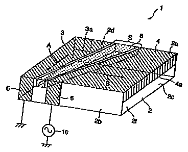
Fig. 1 shows a schematic perspective view showing a
surface-mounted type antenna in accordance with a first
embodiment. The surface-mounted type antenna 1 shown in Fig.
1 has a dielectric substrate 2, and on the top surface 2a of
the dielectric substrate 2, a power non-supplied side
radiation electrode 3 which is a first radiating electrode,
CA 02426497 2003-03-10
- 9 -
and a power supplied side radiation electrode 4 which is a
second radiating electrode are formed with a space
therebetween. In this first embodiment, the space S between
the power non-supplied side radiation electrode 3 and the
power supplied side radiation electrode 4 is formed so that
the longitudinal sides thereof tilt with respect to each
side of the top surface 2a of the dielectric substrate 2
(for example, at an angle of 45 degrees).
On a side surface 2b of the dielectric substrate 2, a
ground electrode 5 connected to the power non-supplied side
radiation electrode 3, and a power supply electrode 6
connected to the power supply radiation side radiation
electrode 4 are each linearly formed from the top surface
side to the bottom surface side.. The power supply radiation
side radiation electrode 4 extends from the top surface 2a
and forms the open end 4a thereof on a side surface 2c of
the dielectric substrate 2, while the power non-supply
radiation side radiation electrode 3 extends from the top
surface 2a and forms the open end 3a thereof on a side
surface 2d.
The space S is formed so as to gradually widen from the
side surface 2b, where the ground electrode 5 and the power
supply electrode 6 are formed, toward the side surface 2d
constituting an open end. The reason for this is as follows.
The ground electrode 5 and the power supply electrode 6 are
CA 02426497 2003-03-10
- 10 -
coupled in an electric field. Therefore, in order to
effectively control the amount of the electric field
coupling, it is effective to widen the space S on the open
end, where a strong electric field exists, that is, the
space S on the side surface 2d side.
A permittivity adjusting material portion 8 which is
the most characteristic capacitive-coupling adjusting means
of the ffirst embodiment is provided in the space S between
the power non-supplied side radiation electrode 3 and the
power supplied side radiation electrode 4. The purpose of
providing the permittivity adjusting material portion 8
shown in the ffirst embodiment is to weaken the capacitive
coupling between the power non-supplied side radiation
electrode 3 and the power supplied side radiation electrode
4. The permittivity adjusting material portion 8 has a lower
permittivity than that of the dielectric substrate 2. In
the example shown in Fig. 1, the permittivity adjusting
material portion 8 is embedded only in the upper side of the
space S between the power non-supplied side radiation
electrode 3 and the power supplied side radiation electrode
4, in the dielectric substrate 2 (that is, only in the area
chiefly concerned to the capacity between the power non-
supplied side radiation electrode 3 and the power supplied
side radiation electrode 4).
The surface-mounted type antenna in according with the
CA 02426497 2003-03-10
- 11 -
first embodiment has the features as described above. Such
a surface-mounted type antenna 1 is mounted onto the circuit
board incorporated in a communication device such as
portable telephone or the like, in such a manner in which
the bottom 2f of the dielectric substrate 2 is mounted on
the circuit board side. The circuit board has a power
supply circuit 10 formed thereon. By mounting the surface-
mounted type antenna 1 onto the circuit board, the power
supply electrode 6 of the surface-mounted type antenna 1 is
connected to the power supply circuit 10.
When a power is supplied from the power supply circuit
10 to the power supply electrode 6, the power is directly
supplied from the power supply electrode 6 to the power
supplied side radiation electrode 4, and the power is
transmitted by the power supply electrode 6 to the power
non-supplied side radiation electrode 3 by virtue of
electromagnetic coupling, whereby the power non-supplied
side radiation electrode 3 and the power supplied side
radiation electrode 4 resonate and perform the function of
an antenna.
As described above, in this first embodiment, the
longitudinal sides of the space S between the power non-
supplied side radiation electrode 3 and the power supplied
side radiation electrode 4 tilt with respect to each side of
the top surface 2a of the dielectric substrate 2, and the
CA 02426497 2003-03-10
- 12 -
ground electrode 5 and the power supply electrode 6 are
disposed adjacent to each other, as well as the open end 3a
of the power non-supplied side radiation electrode 3 and the
open end 4a of the power supplied side radiation electrode 4
are formed on the different side surfaces from each other,
of the dielectric substrate 2. By these features, as shown
in Fig. 1, the resonance direction A of the power non-
supplied side radiation electrode 3 and the resonance
direction B of the power supplied side radiation electrode 4
intersect each other substantially at right angles. This
allows the mutual interference of the resonances of the
power non-supplied side radiation electrode 3 and the power
supplied side radiation electrode 4 to be suppressed, and
enables superior antenna characteristics to be achieved,
without widening the space S between the power non-supplied
side radiation electrode 3 and the power supplied side
radiation electrode 4.
Thus, the mutual interference of the resonances of the
power non-supplied side radiation electrode 3 and the power
supplied side radiation electrode 4 can be substantially
inhibited, by arranging the resonance direction A of the
power non-supplied side radiation electrode 3 and the
resonance direction B of the power supplied side radiation
electrode 4 so as to intersect each other substantially at
right angles. However, when the dielectric substrate 2 is
. CA 02426497 2003-03-10
- 13 -
formed of a material having a high permittivity or is
thinned for the purpose of miniaturization, the above-
described arrangement cannot achieve by itself the capacity
between the power non-supplied side radiation electrode 3
and the power supplied side radiation electrode 4, the
capacity being commensurate with the capacity (fringing
capacity) between the power non-supplied side radiation
electrode 3 and the ground or the capacity (fringing
capacity) between the power supplied side radiation
electrode 4 and the ground. This results in that a mutual
interference of the resonances between the power non-
supplied side radiation electrode 3 and the power supplied
side radiation electrode 4 cannot be completely inhibited.
In contrast, when the capacity between the power non-
supplied side radiation electrode 3 and the power supplied
side radiation electrode 4 is larger than the above-
described fringing capacity, the permittivity adjusting
material portion 8 which has a lower permittivity than that
of the dielectric substrate 2 is interposed between the
power non-supplied side radiation electrode 3 and the power
supplied side radiation electrode 4, in this first
embodiment, as described above, so that the capacity
occurring between the power non-supplied side radiation
electrode 3 and the power supplied side radiation electrode
4 can be made smaller than the case where the entire area
CA 02426497 2003-03-10
- 14 -
between the power non-supplied side radiation electrode 3
and the power supplied side radiation electrode 4 is the
dielectric substrate 2. This allows the capacitive coupling
between the power non-supplied side radiation electrode 3
and the power supplied side radiation electrode 4 to be
significantly weakened.
In this first embodiment, therefore, by providing both
of the arrangement for making the resonance directions of
the power non-supplied side radiation electrode 3 and power
supplied side radiation electrode 4 intersect each other
substantially at right angles, and the arrangement for
weakening the capacitive coupling between the power non-
supplied side radiation electrode 3 and the power supplied
side radiation electrode 4, it is possible to inhibit
substantially surely the mutual interference of the
resonances of the power non-supplied side radiation
electrode 3 and the power supplied side radiation electrode
4, without taking measures such as a reduction of the
permittivity of the dielectric substrate 2, or widening of
the space S between the power non-supplied side radiation
electrode 3 and the power supplied side radiation electrode
4, from the viewpoint of the miniaturization of the
dielectric substrate 2. This allows superior plural-
resonance conditions to be stably achieved and enables
antenna characteristics to be improved.
CA 02426497 2003-03-10
- 15 -
Also, since the space S is wider on the side surface 2d
side constituting an open end, the control of the amount of
the capacitive coupling between the power non-supplied side
radiation electrode 3 and the power supplied side radiation
electrode 4 can be effectively performed, in conjunction
with the adjustment of the capacitive coupling by the
permittivity adjusting material portion 8.
In this first embodiment, since superior plural-
resonance conditions are thus stably achieved, excellent
effects are produced which allow a surface-mounted type
antenna 1 which is small and low-profile and which has high-
reliability antenna characteristics to be provided.
Next, a second embodiment of the present invention will
be described. This second embodiment characteristically
differs from the above-described first embodiment in that,
as shown in Fig. 2, there is provided a groove 12 which is
capacity coupling means, instead of the permittivity
adjusting material portion 8 provided between the power non-
supplied side radiation electrode 3 and the power supplied
side radiation electrode 4. Other features are the same as
those of the first embodiment. In this second embodiment,
the same components as those of the first embodiment have
been given the same reference numerals, and repeated
descriptions of the components in common therebetween will
be omitted.
CA 02426497 2003-03-10
- 16 -
The surface-mounted type antenna in accordance with the
second embodiment is also provided with an arrangement for
weakening the capacitive coupling between the power non-
supplied side radiation electrode 3 and the power supplied
side radiation electrode 4, as in the case of the first
embodiment. Specifically, the groove 12 which characterizes
this second embodiment is provide along the longitudinal
sides of the space S between the power non-supplied side
radiation electrode 3 and the power supplied side radiation
electrode 4, and the magnitude of the groove 12 is one
enough to reduce the permittivity between the power non-
supplied side radiation electrode 3 and the power supplied
side radiation electrode 4 to a small value such as to
inhibit the mutual interference of the resonances of the
power non-supplied side radiation electrode 3 and the power
supplied side radiation electrode 4.
In accordance with the second embodiment, the power
non-supplied side radiation electrode 3 and the power
supplied side radiation electrode 4 are formed so as to
intersect each other substantially at right angles, as in
the case of the first embodiment. In addition, the groove
12 is formed between the power non-supplied side radiation
electrode 3 and the power supplied side radiation electrode
4, whereby the permittivity between the power non-supplied
side radiation electrode 3 and the power supplied side
, CA 02426497 2003-03-10
- 17 -
radiation electrode 4 is made lower than that of the
dielectric substrate 2, and thereby the capacitive coupling
between the power non-supplied side radiation electrode 3
and the power supplied side radiation electrode 4 is
weakened. By such features, in this second embodiment also,
it is possible to reliably inhibit the mutual interference
of the resonances of the power non-supplied side radiation
electrode 3 and the power supplied side radiation electrode
4, and to stably achieve superior plural-resonance
conditions, as is the case with the first embodiment. This
can produce superior effects which allow a surface-mounted
type antenna 1 which is small and low-profile and which has
high-reliability antenna characteristics to be provided.
Next a third embodiment of the present invention will
be described. This third embodiment is characterized in
that, as shown in Fig. 3, hollow portions 14 and 15 as
capacitive-coupling adjusting means are provided within the
dielectric substrate 2. Other features are the same as
those of the above-described embodiments. In this third
embodiment, the same components as those of the above-
described embodiments have been given the same reference
numerals, and repeated descriptions of components in common
therebetween will be omitted:
As illustrated in Fig. 3, in this third embodiment, the
hollow portion 14 is located in the area of the power non-
~
. CA 02426497 2003-03-10
- 18 -
supplied side radiation electrode 3, within the dielectric
substrate 2, while the hollow portion 15 is provided
together with the hollow portion 14 at a distance therefrom.
In accordance with the third embodiment, since the
hollow portion 14 is formed in the area of the power non-
supplied side radiation electrode 3, within the dielectric
substrate 2, the hollow portion 14 allows the capacity
between the power non-supplied side radiation electrode 3
and the ground to be reduced. Also, since the hollow
portion 15 is formed in the area of the power supplied side
radiation electrode 4, within the dielectric substrate 2,
the hollow portion 15 allows the capacity between the power
supplied side radiation electrode 4 and the ground to be
reduced.
Specifically, in the third embodiment, since each of
the fringing capacities between the radiation electrodes 3
and 4 and the ground can be easily varied so as to be
commensurate with the capacity between the power non-
supplied side radiation electrode 3 and the power supplied
side radiation electrode 4, it is possible to adjust the
capacity between the power non-supplied side radiation
electrode 3 and the power supplied side radiation electrode
4 and the above-described fringing capacity so as to have an
proper relationship of being commensurate with each other.
This inhibits substantially surely the mutual interference
~
CA 02426497 2003-03-10
- 19 -
of the resonances of the power non-supplied side radiation
electrode 3 and the power supplied side radiation electrode
4, and allows superior plural-resonance conditions to be
stably achieved, as in the cases of the above-described
embodiments. Thereby superior effects can be produced which
allow a surface-mounted type antenna 1 which is small and
low-profile and which has high-reliability antenna
characteristics to be attained.
As describe above, in the third embodiment, since the
hollow portion I4 is located adjacent to the open end 3a of
the power non-supplied side radiation electrode 3, and the
hollow portion 15 is formed adjacent to the open end 4a of
the power supplied side radiation electrode 4, it is
possible to reduce the permittivity between the power non-
supplied side radiation electrode 3 and the ground, and that
between the power supplied side radiation electrode 4 and
the ground, and is thereby possible to relieve the electric
field concentration between the power non-supplied side
radiation electrode 3 and the ground and that between the
power supplied side radiation electrode 4 and the ground.
This effect coupled with the suppressing effect with
respect to the mutual interference of the resonances between
the power non-supplied side radiation electrode 3 and the
power supplied side radiation electrode 4, can promote
widening of the band width of the surface-mounted type
CA 02426497 2003-03-10
- 20 -
antenna 1 and an increase in the gain thereof.
Next, a fourth embodiment of the present invention will
be described. In the descriptions of this fourth embodiment,
the same components as those of the above-described
embodiments have been given the same reference numerals, and
repeated descriptions of components in common therebetween
will be omitted.
The fourth embodiment is characterized in that, as is
the cases with the above-described embodiments, there is
provided an arrangement for weakening the capacitive
coupling between the power non-supplied side radiation
electrode 3 and the power supplied side radiation electrode
4. Specifically, as illustrated in Figs. 4A and 4B, the
dielectric substrate 2 is formed by bonding first and second
dielectric substrates 17 and 18 which have different
permittivities from each other, and the bonded portion 20
between the first dielectric substrate 17 and the second
dielectric substrate 18 is disposed in the space S between
the power non-supplied side radiation electrode 3 and the
power supplied side radiation electrode 4. Other features
are substantially the same as those of the above-described
embodiments. In this fourth embodiment, the same components
as those of the above-described embodiments have been given
the same reference numerals, and repeated descriptions of
components in common therebetween will be omitted.
CA 02426497 2003-03-10
- 21 -
In this fourth embodiment, the second dielectric
substrate 18 has a lower permittivity than that of the first
dielectric substrate 17, and the first dielectric substrate
17 and the second dielectric substrate 18 are bonded by, for
example, a ceramic adhesive. As illustrated in Fig. 4A, a
power non-supplied side radiation electrode 3 is formed on
the surface of the first dielectric substrate 17, while a
power supplied side radiation electrode 4 is formed on the
surface of the second dielectric substrate 18. In other
words, in the fourth embodiment, a dielectric substrate 2 is
formed by bonding the first dielectric substrate 17 for
forming the power non-supplied side radiation electrode 3
and the second dielectric substrate 18 for forming the power
supplied side radiation electrode 4, the radiation
electrodes 3 and 4 having different permittivities from each
other.
As described above, in the fourth embodiment, the
bonded portion 20 between the first dielectric substrate 17
and the second dielectric substrate l8 is disposed in the
space S between the power non-supplied side radiation
electrode 3 and the power supplied side radiation electrode
4. That is, the first and second dielectric substrates 17
and 18 which have different permittivities from each other,
are disposed between the power non-supplied side radiation
electrode 3 and the power supplied side radiation electrode
~
. CA 02426497 2003-03-10
- 22 -
4. In such a case, the capacity between the power non-
supplied side radiation electrode 3 and the power supplied
side radiation electrode 4 is, of course, related to the
occupation ratio between the first dielectric substrate 17
and the second dielectric substrate 18 in between the power
non-supplied side radiation electrode 3 and the power
supplied side radiation electrode 4, but it is primarily
determined based on the permittivity of the dielectric
substrate having the lower permittivity.
In consideration of this, the bonded portion 20 between
the first dielectric substrate 17 and the second dielectric
substrate 18 is disposed at the position which allows the
capacitive coupling between the power non-supplied side
radiation electrode 3 and the power supplied side radiation
electrode 4 to be weakened, and which thereby enables the
mutual interference of the resonances between the power non-
supplied side radiation electrode 3 and the power supplied
side radiation electrode 4 to be inhibited.
In accordance with the fourth embodiment, the
dielectric substrate 2 is formed by bonding the first and
second dielectric substrates 17 and 18 which have different
permittivities from each other, and the bonded portion 20
between the first dielectric substrate 17 and the second
dielectric substrate 18 is disposed in the space S between
the power non-supplied side radiation electrode 3 and the
CA 02426497 2003-03-10
- 23 -
power supplied side radiation electrode 4.
Providing this construction allows the capacity between
the power non-supplied side radiation electrode 3 and the
power supplied side radiation electrode 4 to be reduced, and
enables the mutual interference of the resonances between
the power non-supplied side radiation electrode 3 and the
power supplied side radiation electrode 4 to be suppressed,
with the result that superior plural-resonance conditions
are stably achieved. This can produce superior effects
which allow a surface-mounted type antenna 1 which is small
and low-profile and which has high-reliability antenna
characteristics to be provided.
Next, a fifth embodiment of the present invention will
be described. In this fifth embodiment, an example of a
communication device provided with one of the surface-
mounted type antennas shown in the above-described
embodiments is illustrated. Fig. 5 schematically
illustrates an example of a portable telephone which is a
communication device. The portable telephone 25 shown in
Fig. 5 has a circuit board 27 provided in a case 26. A
power supply circuit 10, a switching circuit 30, a
transmitting circuit 31, and a receiving circuit 32 are
formed on the circuit board 27. On such a circuit board 27,
one of the surface-mounted type antennas 1 shown in the
above-described embodiments, and this surface-mounted type
' CA 02426497 2003-03-10
- 24 -
antenna 1 is connected to the transmitting circuit 31, and
the receiving circuit 32 via the power supply circuit 10 and
the switching circuit 30.
In the portable telephone 25 shown in Fig. 5, the
surface-mounted type antenna 1 performs the function of an
antenna by receiving the supply of a power from the power
supply circuit 10 thereto, as described above, and the
transmission and reception of waves are smoothly performed
by the switching action of the switching circuit 30.
ZO In accordance with this fifth embodiment, since the
portable telephone 25 is equipped with one of the surface-
mounted type antennas 1 shown in the above-described
embodiments, the miniaturization of the portable telephone
25 can be easily achieved as a result of the size-reduction
of the surface-mounted type antenna 1. Also, a portable
telephone 25 having a high reliability of communication can
be provided since it incorporates therein a surface-mounted
type antenna 1 having superior antenna characteristics as
described above.
Meanwhile, the present invention is not limited to the
above-described embodiments, but various embodiments can be
adopted. Fore example, the shapes of the power non-supplied
side radiation electrode 3 and the power supplied side
radiation electrode 4 are not restricted to the shapes
illustrated in the above-described embodiments, but various
CA 02426497 2003-03-10
- 25 -
shapes can be used. For example, the shapes as shown in
Figs. 6(a), 6(b) and 7(a) can be employed. In the example
shown in Fig. 6(a), the power non-supplied side radiation
electrode 3 and the power supplied side radiation electrode
4 are formed into a meander-shape. The arrangement is such
that a power is transmitted from an meander-shaped end
portion a to the power non-supplied side radiation electrode
3, while a power is transmitted from an meander-shaped end
portion ~ to the power supplied side radiation electrode 4.
The open end of the power non-supplied side radiation
electrode 3 is formed on a side surface 2e of the dielectric
substrate 2, while the open end of the power supplied side
radiation electrode 4 is formed on a side surface 2c.
Forming the power non-supplied side radiation electrode 3
and the power supplied side radiation electrode 4 in this
way, results in that the resonance direction A of the power
non-supplied side radiation electrode 3 and the resonance
direction B of the power supplied side radiation electrode 4
intersect each other at substantially at right angles.
Consequently, as is the cases with the above-described
embodiments, it is possible to substantially inhibit the
mutual interference of the resonances of the power non-
supplied side radiation electrode 3 and the power supplied
side radiation electrode 4.
The example shown in Fig. 6(b) is the one wherein the
CA 02426497 2003-03-10
- 26 -
electrode area on the open end side of the power supplied
side radiation electrode 4 shown in Fig. 6(a) is enlarged,
and wherein the electric field concentration on the open end
side of the power supplied side radiation electrode 4 is
thereby relieved in order to further improve the antenna
characteristics.
The examples illustrated in Fig. 7(a) are shape
examples of the power non-supplied side radiation electrode
3 and the power supplied side radiation electrode 4 which
allow the above-described plural resonance to be created in
a dual-band surface-mounted type antenna 1 which is capable
of transmitting and receiving waves in two different
frequency bands from each other, as shown in the frequency
characteristics in Fig. 7(b) and 7(c). In this example
illustrated in Fig. 7(a), the arrangement is such that the
power non-supplied side radiation electrode 3 and the power
supplied side radiation electrode 4 are each formed into
meander-shapes, that an electrode is transmitted to each of
the meander-shaped end portions a and ~ of the power non-
supplied side radiation electrode 3 and the power supplied
side radiation electrode 4, and that the resonance direction
A of the power non-supplied side radiation electrode 3 and
the resonance direction B of the power supplied side
radiation electrode 4 intersect each other at substantially
at right angles.
CA 02426497 2003-03-10
- 27 -
The power supplied side radiation electrode 4 is formed
by continuously connecting a plurality of electrode portions
4a and 4b which differ in the meander pitch from each other,
and is formed so as to have two resonance frequencies F1 and
F2 such that the frequency bands of waves do not overlap
each other, as illustrated in Figs. 7(b) and 7(c).
The resonance frequency of the power non-supplied side
radiation electrode 3 is set to a frequency in the vicinity
of the resonance frequency F1 of the power supplied side
radiation electrode 4, or to a frequency in the vicinity of
the above-described resonance frequency .F2 so as to have a
plural-resonance relation with the resonance frequency of
the power supplied side radiation electrode 4.
When the resonance frequency of the power non-supplied
side radiation electrode 3 is set to a frequency in the
vicinity of the resonance frequency F1 of the power supplied
side radiation electrode 4, for example, to the frequency
F1' shown in Fig. 7(b), a plural-resonance state is created
at the resonance frequency F1, while, when the resonance
frequency of the power non-supplied side radiation electrode
3 is set to a frequency in the vicinity of the resonance
frequency F2 of the power supplied side radiation electrode
4, for example, to the frequency F2' shown in Fig. 7(c), a
plural-resonance state is created at the resonance frequency
F2.
CA 02426497 2003-03-10
- 28 -
When the construction which characterizes the above-
described first and second embodiments is applied to the
surface-mounted type antenna 1 wherein the power non-
supplied side radiation electrode 3 and the power supplied
side radiation electrode 4 are formed into the shapes shown
in Fig. 6(a), 6(b), or 7(a), a permittivity adjusting
material portion 8 or a groove 12 is provided, for example,
as indicated by the dot lines in Figs. 6(a), 6(b), or 7(a).
Furthermore, for example, when the construction which
characterizes the above-described third embodiment is
applied to the surface-mounted type antenna 1 which is
formed into the shape shown in Fig. 6(b) or 7(a), hollow
portions 14 and 15 are formed within the dielectric
substrate 2, for example, as indicated by the dot lines in
Fig. 8(a) or 8(b). Moreover, when the construction which
characterizes the above-described fourth embodiment is
applied, the dielectric substrate 2 is formed by bonding the
first dielectric substrate 17 which is used for forming the
power non-supplied side radiation electrode 3, and the
second dielectric substrate 18 which has a lower
permittivity and which is used for forming the power
supplied side radiation electrode 4, for example, as shown
in Figs. 8(a) and 8(b).
In the above-described embodiments, the arrangement is
such that a power is directly supplied from the power supply
CA 02426497 2003-03-10
- 29 -
electrode 6 to the power supplied side radiation electrode 4,
but it may be such that the power supplied side radiation
electrode 4 and the power supply electrode 6 is non-
connected to each other, and that a power is supplied from
the power supply electrode 6 to the power supplied side
radiation electrode 4 by means of.capacitive coupling.
In the above-described first embodiment, the width of
the permittivity adjusting material portion 8 is narrower
than that of the space S between the power non-supplied side
radiation electrode 3 and the power supplied side radiation
electrode 4. However, as shown in Fig. 9, the width of
permittivity adjusting material portion 8 may be arranged so
as to be wider than that of the space S so that the power
non-supplied side radiation electrode 3 and the power
supplied side radiation electrode 4 are formed astride the
edge portions of the permittivity adjusting material portion
8.
In the above-described second embodiment, the groove 12
is provided in the space S between the power non-supplied
side radiation electrode 3 and the power supplied side
radiation electrode 4, but, for example, a recess without an
opening may be formed on the side surfaces 2b and 2d,
instead of the groove 12. Furthermore, a plurality of
recesses as capacitive-coupling adjusting means may be
arranged with a space therebetween.
~
. CA 02426497 2003-03-10
- 30 -
In the above-described third embodiment, the two hollow
portions 14 and 15 are provided, but only one of these
hollow portions 14 and 15 may be formed. Also, the shape of
the hollow portions 14 and 15 is not limited to the one
shown in Fig. 3, but various shapes may be adopted. For
example, the hollow portions 14 and 15 shown in Fig. 3 pass
through the dielectric substrate from the side surface 2b to
the side surface 2d, but they may be closed hollow portions
without openings. Furthermore, the hollow portions 14 and
15 may be recesses or groove-shaped hollow portions such
that the bottom 2f side of the dielectric substrate 2 is
open.
Among the construction wherein a permittivity adjusting
material portion is provided as shown in the first
embodiment, the construction wherein a groove or a recess is
provided as shown in the second embodiment, the construction
wherein hollow portions are provided as shown in the third
embodiment, and the construction wherein the dielectric
substrate 2 constitutes a bonded body of a plurality of
dielectric substrates which differ in the permittivity from
each other as shown in the fourth embodiment, two or more
constructions may be combined to use.
Furthermore, in the above-described fifth embodiment,
although the one example of a portable telephone as a
communication device is shown, this invention is not
' ~ CA 02426497 2003-03-10
- 31 -
restricted to portable telephones, but can be applied to
communication devices other than portable telephones.
In the above-described embodiments, descriptions have
been made of the construction for weakening the capacitive
coupling between the power non-supplied side radiation
electrode 3 and the power supplied side radiation electrode
4. However, when the capacity between the power non-
supplied side radiation electrode 3 and the power supplied
side radiation electrode 4 is significantly smaller than the
above-described fringing capacity, it is preferable to
increase the capacity between the power non-supplied side
radiation electrode 3 and the power supplied side radiation
electrode 4 so as to be commensurate with the fringing
capacity, and to thereby strengthen the capacitive coupling
between the power non-supplied side radiation electrode 3
and the power supplied side radiation electrode 4.
In such a case, there is provided capacitive-coupling
adjusting means for strengthening the capacitive coupling
between the power non-supplied side radiation electrode 3
and the power supplied side radiation electrode 4. For
example, as indicated by the dot lines in Fig. 7(a) and as
illustrated in Fig. 9, the following permittivity adjusting
material portion 8 as capacitive-coupling adjusting means is
provided in the space S between the power non-supplied side
radiation electrode 3 and the power supplied side radiation
. CA 02426497 2003-03-10
- 32 -
electrode 4. This permittivity adjusting material portion 8
is formed of a material having a higher permittivity than
that of the dielectric substrate 2. It is, therefore,
possible to make the permittivity between the power non-
supplied side radiation electrode 3 and the power supplied
side radiation electrode 4 larger than that of the
dielectric substrate 2, and to thereby adjust the capacity
between the power non-supplied side radiation electrode 3
and the power supplied side radiation electrode 4 to become
a capacity which is commensurate with that of the above-
described fringing capacity. Meanwhile, in the case where
the power non-supplied side radiation electrode 3 and the
power supplied side radiation electrode 4 have shapes as
shown in Fig. 9, it is preferable that each of the power
non-supplied side radiation electrode 3 and the power
supplied side radiation electrode 4 be disposed astride the
side edges of the permittivity adjusting material portion 8.
Also, the power non-supplied side radiation electrode 3
and the power supplied side radiation electrode 4 may be
formed into shapes as shown in Fig. 11 so that the space S
between the power non-supplied side radiation electrode 3
and the power supplied side radiation electrode 4 is
narrowed, and that the capacity between the power non-
supplied side radiation electrode 3 and the power supplied
side radiation electrode 4 is increased so as to become a
CA 02426497 2003-03-10
- 33 -
capacity which is commensurate with that of the above-
described fringing capacity, by enlarging the areas of the
opposing electrodes.
As described above, when satisfactory plural resonance
conditions cannot be achieved because the capacity between
the power non-supplied side radiation electrode 3 and the
power supplied side radiation electrode 4 is significantly
smaller than the fringing capacity, the capacity between the
power non-supplied side radiation electrode 3 and the power
supplied side radiation electrode 4 and the fringing
capacity can be brought into a proper matching relation, by
adjusting the capacity between the power non-supplied side
radiation electrode 3 and the power supplied side radiation
electrode 4 to increase so as to become a capacity which is
commensurate with the fringing capacity by means of the
above-described capacitive-coupling adjusting means for
increasing the capacity between the power non-supplied side
radiation electrode 3 and the power supplied side radiation
electrode 4. Hence, it is possible to suppress the mutual
interference of the resonances between the power non-
supplied side radiation electrode 3 and the power supplied
side radiation electrode 4, which results in superior
plural-resonance conditions.
Also, the power non-supplied side radiation electrode 3
and the power supplied side radiation electrode 4 may be
' CA 02426497 2003-03-10
- 34 -
formed within the dielectric substrate 2. In this case, as
the dielectric substrate 2, a multilayer subs rate formed by
laminating a plurality of ceramic green sheets may be used.
Ceramic green sheets having a different permittivity from
that of the above-mentioned ceramic sheets may be provided
between the power non-supplied side radiation electrode 3
and the power supplied side radiation electrode 4, for use
as capacitive- coupling adjusting means.
As described above, in accordance with the present
invention, when capacitive-coupling adjusting means is
provided, and the strength of the capacitive coupling
between the first radiation electrode and the second
radiation electrode is varied by making the permittivity in
the space which is situated between the first radiation
electrode and the second radiation electrode and in which a
capacity occurs, differ from that of the dielectric
substrate by means of the above-described capacitive-
coupling adjusting means, the mutual interference of the
resonances between the first radiation electrode and the
second radiation electrode can be inhibited. It is,
therefore, possible to stably achieve superior plural-
resonance conditions without taking measures such as a
reduction of the permittivity of the dielectric substrate or
widening of the space S between the first radiation
electrode and the second radiation electrode, the measures
CA 02426497 2003-03-10
- 35 -
inhibiting the miniaturization of the dielectric substrate.
In addition, from the viewpoint of thinning, it becomes easy
to attain a capacity between the first radiation electrode
and the second radiation electrode which is commensurate
with each of the capacities between the above-mentioned two
electrodes and the ground, which allows the degree of
freedom of design to be improved.
Since superior plural-resonance conditions are thus
stably achieved, a surface-mounted type antenna which is
small and low-profile and which has high-reliability antenna
characteristics can be provided.
When a recess or a groove which is capacitive-coupling
adjusting means is formed, when a permittivity adjusting
material portion which is capacitive-coupling adjusting
means is formed, or when hollow portions which are
capacitive- coupling adjusting means are formed, the
strength of the capacitive coupling between the first
radiation electrode and the second radiation electrode can
be varied by a simple construction, whereby superior effects
as described above are produced.
When the dielectric substrate constitutes a bonded body
of the first dielectric substrate and the second dielectric
substrate which differ in the permittivity from each other,
the first radiation electrode is formed on the first
dielectric substrate while the second radiation electrode is
CA 02426497 2003-03-10
- 36 -
formed on the second dielectric substrate, and a bonded
portion between the first dielectric substrate and the
second dielectric substrate is provided between the first
radiation electrode and the second radiation electrode, it
is possible to vary the permittivity between the first
radiation electrode and the second radiation electrode, as
in the case described above. This allows the mutual
interference of the resonances between the first radiation
electrode and the second radiation electrode to be
suppressed, and enables a surface-mounted type antenna which
is small and low-profile and which has high-reliability
antenna characteristics to be provided. In addition, the
degree of freedom of design can be improved.
In a communication device which is provided with the
surface-mounted type antenna which produces above-described
effects, it is possible to easily promote the
miniaturization of the communication device as a result of
the size-reduction of the surface-mounted type antenna, and
also possible to improve the reliability of communication.
Industrial Applicability
As is evident from the above descriptions, the surface-
mounted type antenna and the communication device provided
therewith are applied to, for example, surface-mounted type
CA 02426497 2003-03-10
- 37 -
antennas and the like to be mounted on the circuit boards
incorporated in communication devices such as portable
telephones.