Note: Descriptions are shown in the official language in which they were submitted.
CA 02428973 2003-05-16
OPTICAL ELEMENT USING ONE-DI1~NSIONAL PEtOTC)NIC CRYSTAL AND
SPECTRQSCOPIC DEVICE USING TFiE SAID
The present application is based,on Japanese ~'atent
Application No. 2002-142449, the entire contents of which axe
incorporated herein by reference.
BACKGROUND 0~" THE INVENTION'
7.. Field of the Invention
The present invention relates to an optzca~. Qlement,
especially a wavelength dispersion element used in an optical
communication system, an optical measuring system, etc.
2. Related Art
It is known T.~e? 1 that photonic crystals having a str~xcture
in which dielectric materials differe~xt ir. refractive index
are arranged period~.cally at intervals o~ about a wave~_engtb.
of light has the following properties:
(a) confinement of lierht by photonic Jand gaps;
(b; vexy large wavelength dispersion due to a tt:nique
photonic bard s~.Yucture; and.
i,c; tarrorr::w-.:S.ty in group velocity cf propagated light.
Tar i c~vs -~pricai e.iements using these properties have bLen
p.rcpose;~,
~~-oten.c crystals can be classified into three groups
by th.~-.. raumos_~- ov directions having periodic structures as
i=c~~.? ~.=~rs
i;~ o~ae-dimensional photonic crystals;
CA 02428973 2003-05-16
(ii) two-dimensional photanic crystals> and '
(iii) three, dimensional photonic crystals.
For examplef the simplest one-dimensional photanic
crysta l l s a dzelectr zc multilayer filter formed in such a manner
that two kinds of thin films (e.g., Sio2 and Tia2) are laminated
alternately on a parallel-plane substrate. The dielectric
multilayer filter has been already put into practical use.
Because this structure has photonic band gaps in the periodic
direction, this structure has a function of reflecting only
incident light of a specific wavelength region,. Furthermore,
because the wavelength region in the photonic band gap with
respect to oblique incident light vax'ies according to the
directionofpolaxization, this structure can. be made to function
as a polarized l,igk~t separating filter.
~.lthcuc~h the one-dimensional photonic crystal has a large
merit that it is easy to produce, the one-dimensional photonic
crystal has not beer_ investigated as much as two-dimensional
arad three--dimensional photonic crystals because there are few
methods making good use of the properties of photonic crystals
2C except the aforementianed filter. The one-dimensional
photonic crystal, however, can use the property of "~rary large
wa~relength dispersion due to a unique band structure" yr
"abnormality in group velocity of propagated light'°
suffiCie?~t?;~ though the one-dimensional. photonie crystal is
infe riar in the funct5.an of '°conf~.nement of light by photonic
2
CA 02428973 2003-05-16
band gaps" to two-dimensional and three-dimensional photonic
crystals. As means using the property, there is an example
in which an end surface of the multilayer film, that is, a surface
on which the mul tilayex structure is exposed is used as a light
input surface ar as a light output surface.
For example, theoretical analys~.s of the direction of
light rays znca~dent onto an inclined section of the multilayer
film has been described in Appl~.ed Physics B, Vo1.39, p.23~.,
198 6. There has been disclosed the fact that the same polarized
light separating effect as in a birefringent material can be
obtained by use of the property (so-called structural
birefringence) that the refractive index of the multilayer filan
varies widely according to whether the polarization is TE
polarization or Txi polarization, with intention of separating
1.5 polarized light by structural birefringence (Optics vetters,
Vol . I5, No . 9, p . 516, 1990 ) . There has been further a, report
that very large dispersion (super-px°ism effect i can be obtained
because the shape of 4he first photonic band of the peri odic
multilayer film is linear in a ne~.ghbor of a band gap
("International Workshop on Photonic and ~J.ectromagnetic
Crystal Structures" Technical Digest, F1-3).
?~ structure in which aix~ holes are arranged in a thin
film on a substrate by appli catian of photolithac~raphy has been
already examinadwel i as a structure of two-dimen.siona.l photonia
crystal_ If a linear defect is formed in the arrangement of
3
CA 02428973 2003-05-16
the air holes, the portion of the la.near defect can be provided
as an optical waveguide.
If the photonic band gap is provided throughout all
directions zn three-dimensional photonic crystal, a
three-dimensional waveguide can be provided. Accordingly,
there is expectation that a large number of optical elements
can be incorporated in an element about 1 met square when
three-dimensional photonac Crystal is used.
A spectrascop~.c element using phatonic crystal is also
called super-prise. Very large wavelength dispersion cax~ be
obtained compared with a general pxism or diffiraction grating.
nor ex~.~npie, Physical Rev~.ew B, Vol.a$, ~To.l6, p.R1096, 1998
has reported an experimental result that angular dispersion
per ? o wavelength dimference iwuse of three-dimensional
i5 photoni c crystal amounts to tens of degxees. When, for example,
a material large in wavelength dispersion is used as a
spectroscopic element for separating a signal containing
different wavelengths in wavelength division multiplexing
(WDM) communication, the size oz the device as a whole can be
reduced to be very small_
Incider_tally, when photonic crystal is tc be used as a
practical spectroscopic element, there are several pro~rlems.
Parallel light flux is spread at a certain angle by a
diffraction phenomenon. The spread of light flux becomes wide
as the light flux becomes thin. It is therefore preferable
4
_. _ ...
CA 02428973 2003-05-16
that the light flux is thick sufficiently to obtazn a
spectroscopic element with high wavelength resolving power.
Conversely, i.f the light flux is thin, even a spectroscopic
e7.ement large in angular difference due to wavelengths cannot
exhibit high resolving power.
To secure such thick light flux, the size of the element
must be large to a certain degree . In addition, it is inevitable
that the length of the optical path, of light propagating in
the element becomes long. It is however difficult to produce
a large element in the case of two-dimensional or
three-dimensional photanic Crystals. E°urthermore,
attenuation of light in the elements often exhibits a large
value. Accordingly, it is difficult to form a practical
spectroscopic element.
SUMMARY OF THE INVENTTON
The invention is developed to solve the problems and an
obj ect of the invention is to provide a spectroscopic elEment
large in wavelength dispersion. Another object of the
inver_tion is to provide a small.-szze spectroscopic device using
the spectroscopic element.
In the invention, a spectroscopic element large in
wavelength dispersion is obtained in such a manner that light
is input in an. aperiodic direction of a one--dimensiQna3, photonic:
crystal. (periodic structural muitzlayer fzlm) processed znto
a prismatic si~ape, so that wave due to a high-order band is
5
CA 02428973 2003-05-16
propagated through the photonic crystal to thereby obtaia-a laxc~e
wa~reler_gth dispersion. Because a method for pxoduczn.g such
a periodic rnultilayer film has been already estai~7.zsl:~ed,
large-area periodic multzlayer films can be mass-produced.
The aforement~.oned operation is achievedby the following
means.
An optical element using one-dimensional photonic
.. crystal according tc the in~,Yan tior~ ir~cludG:~ a multiyaye-r. .
structure at least one portion of which is a periodic structural
~.0 portion regarded as a one-dimensional photonic crystal having
a predetermined period.. The multilayer structure has t:wo end
surfaces substantially perpendicular to layer surfaces of the
anultilayer structure. One of the two end surfaces is used as
a 1 fight input s;zrface and the other is used as a light output
surface . The light output surface is inclined at an inclination
angle to the light input surface. Directions of prapagation
tiP input beams incident onto the light input surface, beams
propagated in themultilayer structure and output beams emerging
from the light output surface are set to be perpendicular to
a periodic direction of the periodic structural port=ion.
r~ periodzc structural xnulti? aver film ~_s processed into
a prismatic shape to thereby a.chie~re the optical elemer_t having
the aforern.entioned structure.
preferably, a phase modulation unit is provided add scent
or abutting to the light input surface. When input light is
6
CA 02428973 2003-05-16
phase-modulated by the phase modulation unit in the same period
and direction as those of the photonic crystal, only specific
high-order band light can be propagated.
Preferably, in this ease, a phase modulation unit is
further providedadjacent or a3auttingto the light output surface.
By the phase modulation unit, the propagated high-order band
light can be output as a plane wave.
Preferably, a reflecting layer is provided on one or each
of opposite surfaces oz the multilayer structure parallel to
the layer surfaces of the multilayer structure . The reflecting
layer can be achieved by a periodic multilayer film. The
formation oz the reflecting layer can prevent light propac~ati,ng
in the optical element froze e7nerging as a loss fromother surfaces
than. the light output suxface.
Preferably, l.Lght capable of propagating as wave
belonging to the second lowest coupled photanic band i~; used.
as the light propagated through the periodic structural. portion.
spectroscopic device using the optical e? ement includes
the optical elezz~ent, a light input optical system for inputting
a wavelength di~rijion multiplexing optical signal to a light
l nput surface of the aptical element, and a light output optical
system for discriminating optical signals spectroscopi,cally
output from the opti cal element in accordance with wavelengths.
Preferably, the light input optical system includes a
coilizn.atir_g aril t for converting input beams into paral~.el ~>eazns .
r
CA 02428973 2003-05-16
By the collimating unit, broad input light can be obipazz~ed,
so that the angular resolving power of the spectroscopic device
can be impxaved.
Preferably, the light input optical system includes: a
linear optical waveguide or optical. fa.ber for guiding the
wavelength divisicin multiplexing optical signal d a slab optzcal.
waveguide having an input end connected to a light output end
of the linear optical waveguide or optical fiber, and an output
end connected to the light input surface of the optical el_emen~C;
and a beam-condensing element provided in the slab optical
waveguide ror converting propagated beams into parallel beams .
Preferabl y, the light output optical system inc:Ludes a
light coupling unit fo.r coupling the optical signals
speGtroscopicallyoutput from the optical element to aplurality
of light propagation ;.nits. Especially preferably, the light
output OptiGdl system i ncludes : a slab optical waveguide having
an input end connected to the light output surface of the optical
element; a plurality of linear optical waveguidas or optical
fibers connected to an output end of the slab optical waveguide~
and a beam-condensing element provided in the slab optical
waveguide ior. coupling propagated beams to the plurality of
linear optical waveguides ar optical fibers.
Preferably, the beam-condensing element is a waveguide
lens which is provided in the slab optical waveguide and which
is a portion different in refracti~re index from the slab optical
8
CA 02428973 2003-05-16
waveguide and shaped like a lens. or the beam-condensing
element is a diffraction lens pxovzded zn the slab optical
waveguide. Or the beam-condensing element as formed as a
stxueture izx which a boundary surface between. the slab optical
wavegunde and the light input surface or light output surface
o.f the optical element is formed as a curved surface.
$RZEF D~scRZp~z~~r o~° ~xE ~~wz~r~s
F°ig. 1 is a typical view showing propagation of light
in a periodic multilayer filmy
Fig. 2 is a graph showa.ng a photonic band structure (TE
polarization) of the periodic multilayex fiJ.m;
~ig. 3 is a graph showing a photonic band structure ('fM
poJ.arizatian) of the periodic multilayer film;
rF lg. 4 is a view showing a state of refraction of light
in a one-dimensiona:~ photonwc cxysta~. having a triangular prism
structure;
fig. 5 is a typical vie9.~ showing electric field ire first
photo~ic band propagation light;
Fig. 6 is a typical view showing electric field in
high--order coupled photoz~zc band pxopagatzan lighto
rig. 7 is a typical view showing light propagating in
a periodic multilayer .film provided with a phase grafting;
Fig. 8 is a t~apical view showing the case whexe phase
gratings are provided on an input side and an output side
respectivelyp
9
CA 02428973 2003-05-16
Fig. 9 is a view for explaining parameters of respective
portions in the configuration that a phase grating is disposed
on an input side;
Fig. 10 is a typical view showing the case where a wave
obtained by interference of two plane waves is used as input
I1 ght ;
~"ig. 11 is a typical view showing the case where a wave
obtained by interference of three plane waves is used as input
light;
1~ Fig. ~.2 is a typical ~riew showinr~, a structure in which
reflecting layers are provided on opposite surfaces of a
multilayer film;
Fig. 13 is a typical view showing a structure in which
other muitilayer films are provided as reflecting lagers on
opposzte surfaces of a multilayer film;
Figs. 14.~ and 14B are ~r:iews for explaining the band
condition of the one-dimensional photonic crystals provided
for confir_ement o~' 1 fight;
Fig. 1S iv a conceptual view of a spectrascc~pic element
using a one-dimensional photonic crystal having a triangular
prism structure according to the inventions
fig. 1~ a.s a typical view showing a wavegu.ide type
demultiplexinglmultiplexing element using a triangular
prism-shaped ore-dimensional phc~tonic crystal according to the
invention;
,.:. "., ...,. _.,
CA 02428973 2003-05-16
Fig. 17 shows an example in which each boundary surface
between the one-dzznensional photonic crystal and a slab
waveguide is formed as a curved surface;
Fig. 18 is a view for explaining the condition of a
calculation example of a spectrpscopic element using a
triangular prasm-shaped one-dimensional photonic crystal;
Figs. 19A and 19B are views for explaining a method of
conversionally calculating the thickness of a phase grating
at obliaue incidence of l.iaht
Fig. 20 is a graph showing band charts cf the
one-dimensional photonic crystal and the effective refractive
index thereof according to each band chart;
Figs. 2iA to 21L are views showing a result of
electromagnetic wave simulation of refractedlight with respect
to light obliquely incident onto the one-dimensional photonic
crystal (in the case where zxo phase grating is provided);
Fig.. 22 is a view showing a result of another
electromagnetic wave simulation concerning confinement of
light in the X-axis direction (in the case where no phase grating
is proyrided)
fig. 23 is a view showing a result of another
electromagnetic wave simulation concerning confinement of
light in the ~'-axis direction (in the case where no phase gy-ating
is provided):
Figs. 24A to 24C are views showing a result of another
1m
CA 02428973 2003-05-16
electramagnetic wave simulation of refractedlight with respect
to light obliquely incident onto the one-dimensional photonic
crystal (in the oase where no phase gratzng is provided);
Figs. 25A to 25C are views showing a result of another
electromagnetic wave simulatian of refracted light with respeot
to light obliquely inoident onto the one-dimensional photonie
crystal (in the case where no phase grating is provided);
k',ngs. 2~A and 26B are views showing a result of
e~.ectromagnetic wave simulatian of refracted light with respect
to light obliquely incident onto the one-dimensional photonzc
crystal (in the case where phase gratings are provide:d);
Figs . 27A and 27B are views showing a result of another
electromagneticwave simul ation of refracted light with respect
to light obliquely incident onto the one-dimensional photonic
crystal (in the case where phase gratings are provided)r
Figs. 28A and 28B are views showing a result of another
electromagnetzcwave simuJ.atzon of refracted light with respect
to ~.ight obliquely incident onto the one-dimensional photonic
crystal (in the case where phase gratings ax'e provided);
Figs. 29A and 29B are views showing a result of another
elec txomagnetic wave simulation of re fracted :light with r;~spect
to light obliquely incident onto the one-dimensional photonic
crystal (in the case where phase gratings are provided);
Figs. 3aA and 3c~B are views showing a result of another
2~ electromagnetic wave simulation of refractedlzghtwith respect
1. '?
CA 02428973 2003-05-16
to light obliquely incident onto the one-dimensional photonic
crystal (in the Case where phase grat~.rgs are provided)
Figs. 31A and 31B are views showing a result of another
electromagnetic wave simulation of refracted light w~.th respect
to light obliquely incident onto the one~dimensionaJ. photonic
crystal (in the case where phase gratings are provided);
Fig. 32 is a view showing a result of~~another
electromagnetic wave simulation concerning confinement of
lzght in the Y-axis direction (in the case where phase gr,~ti,ngs
are provided); and
Fig. 33 is a view showing a result of another
electromagnetic wave szznu.'.Gtaon concerning confinemer.~t of
light v:.n the Y--axis direction (in the case where phase gratzngs
are provided) .
DETAILED DESCf,.IPTION OF THE PREFERRED EMBODIMENTS
Fanbadiments of the invention will be described below i
specifically.
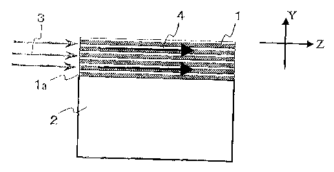
Fig. 1 is a sectional view typically showing a periodzc
multi.layer filmconstitutingabaszc structure of the invention.
i
Aperiodic multilayer film 1 is formed on a surf ace of a sub strate
i
2. For example, the multilayer film is formed as a structure
i
in which layers of a substance A (refractive index: nA) with ',
a thickness of t~ and ~..ayers of a substance B (refractive index:
nB) with a thickness of to are laminated altewnately at intervals
of a period a = f t~ ;- ta) , Assume that a front surface of the
13
CA 02428973 2003-05-16
multilayer film 1 abuts on air.
When input light flux ~ with. a wavelength of ho in a vacuum
is incident onto an end surface la of the pari odic multalayer
film in ~'i.g . 1, how the light propagates in the multilayer film
is o.nalyzed. I t is found from the analysis that the periodic
multilayer film in a predetermined condition serves as so-called
photoni.c crystal, to make propagated light 4 exhibit a unique
effiect.
The characteristic of light propagating in photonic
1Q crystal can be found wi~e:z photonic bands are calculated and
mapped. for example, a method of band calculation has been
described in detail in "Photonic Crystals", Princeton
University Press (1995) or Physical Review B, Vo1.44, hTo.l6,
p.8565, 1991. t
f
assume now that the periodic ~nultii.ayer film shown in
V
~'ig. 1 has a periodic structure continuing infinitely :~ n a ~'
direction (larninatinq direction) and spreads infinitely in X
and Z directions (spreading directions of layer surfaces).
Figs. 2 and 3 show results of band calculation concerning first,
l
2g second and th~.rd photonic bands in '~E poZariaation (Fi.g. 2)
and TM polarization ; Fig. 3) by~ a plane wave method in the Z-axis
l
direction (or the X-axis. direction) about the multilayex~
stxuctare ire whzch layers with refractive index na and layers
with wefractive iz~dea ng axe laminated alternately at regular
inte..vd.~s of a peryod a.
1 d :II
CA 02428973 2003-05-16
na = 1.44 (t~, = 0.5a)
nB = 2.7.8 Et~ = 0.5a)
In Figs. ~ and 3, TE polarization expresses polarization
in the case where the direction of electric field is the :K-axis
direction, and 'I'M polarization expresses polarization in the
case where the direction o:~ magnetic field is the X~s.xis
direction.
i.n each of Figs. 2 and 3, the horizontal axis shows the
magnitude of a wave vector kz in the Z-axis directioxz, and the
verti cal axis shows a normalized frequency represented by the
expression:
wa/2~cc
in which w is an angular Frequency of incident light, a is a
period o~ the structure, and c is a velocity of light in a vacuum.
Because the normalized frequency can be also expressed
as a/A~ in which AQ is the wavelengi~h of incident light in a
vacuum, the normal~.zed frequency will be hereinafer described
as a/Ao. Because there is no periodicity in the Z-axis d~.xection,
the horizontal axis in. each of Figs. 2 and 3 spreads infinitely
without any Brillouin zone boundary.
~.s shown in Fig. 2, when the wavelength of incident light
is h~, in a vs.cuum, a wave vector icR~, corresponding to the first
lowest band i.s present in the photonic crystal . In other words,
the light propagates as a w~.v~e with wavelength h~l ~ 2~r/kA~,
(hereinafter referred to 3s first pPiotonic band light) .in the
CA 02428973 2003-05-16
Z-axis direction in the photonic crystal.
On the other hand, when the wavelength of incident light
is ~.a in a vacuum, wave vectors kH~ and ke2 corresponding to the
First and third photonic bands axe present in the photonic
crystal. In this case, the second phvtanic Qand is neg?_ected
because the second photonic band is an "uncoupled" band with
respect' to propagation in the Z-axis directi on. ~fi.ccord~_ngly,
a wave with wavelength ~H; = 2 ~r JkHl as the First photonic band
~.ight and a wave with wavelength 3~B3 = 2~c'/k~,3 are propagated
in the Z-axis direction in the photor~ic crystal . Other coupled
photonic bands such as the third photonic band in Fig. ? than.
the first photonic band are hereinafter generally refar:red to
as "high-oxder propagation bands". Generally, one of the
second and third photonic bands is a coupled photonic band and
the other is an uncaupJ.ed band» The f.rst photonic band is
a coupled photonic band. Incidentally, the theory of uncoupled
bands has been described in detail in the following nook.
K.Sakoda "optical Properties of Photonic Orystals"
Springer-Verlag (20~J1).
Now, a x~umexzcaJ. value obtained by dividing a wave~.ength
iap, Via, etc. ~ in a vacuum by a corresponding wavelength (hpl.
.h83, etc.) ~.n the phatonic crystal is defined as °'effective
refractive index". As ~.s to be understood froze fig. 2, a/Ao
(vertical axis) and kz (horizon.tal axis) in the first photonic
band light are substantially proportional to each other.
16
CA 02428973 2003-05-16
Accordingly, the effective refractive index in the first
phatonic band Light is substantially constant regardless of
the change of ho. The effective refractive index in 'the
high-order propac~ati.on band light, haweverr varies widely
according to ~o. As i s obvious from Figs. 2 az~d 3, there is
a possibility that the effective refractive index in the
high-order propagation band light may be lower than 1.
Fig. 4 shows a one-dimensional photonic crystal 20 having
a triangular prism structure. Each of end 5urfaGes Ia and 1b
for inputting and outputting light flux is perperddicular to
layer surfaces of the periodic multilayer film 1, that is,
parallel to the periodic direction (Y-axis direction). The
end surfaces Ia and 1b form a predetermined angle therebetw2en.
When input light flux 3 as a plane 'wave is obliquely incident
onto the end suxface za, refraction coxrespondinc~ to the
effective refractive index occurs. AJ.thaugh the firstphotoni::
band light exhibits only wavelength dispersion substantially
equivalent to that of a general homogeneous medium, the
high-order propagation band light exhibits very large
wavelength dispersion because the effective xefxactive zx~dex
varies largely according to the input wavelength as described
above. It can be said that this is a kind of super-prism effect.
When the prism effect for the high-oxder propagation band
light is to be used by the cax~fic~u:rat:.on shown in Fig. 4, there
2~ are however some problems.
17
CA 02428973 2003-05-16
~s is obvious froze Figs. ? and 3, the first p~.oton~.c band
light i.s aJ.ways propagated when the h? gh--order propagatian band
light is propagated. When the high-order propagation band
light is used, the first photonic band light serves as stray
light which causes lowering of the signal to noise ratio o.f
the element as we~.l as the first photonic k~and light is an energy
loss which causes greater reduction in efificiency in use of
the input light.
Furthermore, the periodic structure in the Y-axis
diz:ectian is exposed at the output side end surface 1b in Fig.
9. Cn the other hand, the high-order propagation band light
per sE has periodicity of intensity and phase in the Y-axis
direction. ~ccordingiy, because light rays diffracted in
various orders are mixed as output light, the output Light is
harder to handle than a simple plane wave.
Furthermore, when. the effective refractive index in the
high-order propagation Land light is lower than the refractive
index of one of upper and Iower media abuttia~g on the prism,
propagated light is leaked to the medium side by refraction.
2a Particularly when the effective refractive index in the
high-order propagatian band light is lower than 1, the leakage
cannot be prevented even in the case where the medium is air.
Incidentally, accarding to the inventors' examination,
it has become clear that only specific high-order propagation
band i.ight can Le propagated through the one-dimensiana~
18
CA 02428973 2003-05-16
photonic crystal if input light is phase-modulated.
~'i.gs. 5 and 6 typically show the electric field intensity
of light propagated an the Z-axis direction in the
one-dimensional photonic crystal (period; a) in which layers
of a substance A and lovers of a substance B axe laminated
alternately. In each of Figs. 5 and 6, the solid lines Shaw
peaks of electric field, the broken. lines show troughs of
electric field, and the thickness of each line shows the
magnitude of amplitude.
la As shown in Fig. 5, the first photonic band light
propagates like a plane wave because peaks and troughs of
electric field form planes perpendicular to the 2 axis
respectively, although the amplitude of electric field ix~ the
medium A (5a) is different from that in tre medium s (5b).
Tn case o~ tha high-order propagation band light, however,
"nodes"' in which the amplitude of e? ectric field becomes zero
are generated, for example, as shown in Fig_ 6. As a result,
one period is divided 'into two regions _ peaks and troughs appear
alternately in adj acent regions because the phase of wave shifts
btr a half wavelength between adjacer_t regions. the case where
two nodes are generated in one period as described abo~re is
the case of the second or th~.rd photonic band. 3n propagated
light due to a higher-order band, the number of nodes generated
in one period becomes so larger that the phase shift of a half
wavelength i s repeated by a plural zty of times in one period.
19
CA 02428973 2003-05-16
Accordingly, propagated light rays corresponding to
input light with a wavelength (e. g., Ae in Fig. 2y in which
a plurality of bands are concerned o~rer~.ap each other so that
a complex electric .field pattern is exhibited.
Incidente.lly, when a plane wave 7 is incident onto a phase
modulation unit 6 which is pra~rided for generating a difference
of about a half wa~relength in one period a in the ~'-axis direction
as shown in Fig. 7, an electric field pattern similar to that
of the high-order coupled photonic bazzd ~.z~ Fig. 6 caxa be formed
in a space 8. From the ir_ventors' simulation, it has became
cleax that only the high-order propagation band. 1i ght can be
generated w~.thout generation pf propagated light due to the
first photonic band when an end surface of the one-dzmensional~
photdnic crystal is disposed ~.n the space 8. 'rhe result can
~.S be generalized as follows.
"Then a suitabia phase-modulatEd wave having a period
a in the same direction as the periodic direction of a multilayer
film with a period a is incident onto the multilayer film,, only
propagated light belonging to a specific band can be obtained.'°
If the cptical path is assumed to be reversed, i t is obvious
that propagated light belonging to a specific band ca.n be
returned to a place ware ~ after output from an end surface
of the mu? tilayer fi lm 1 when a suitable phase modulation unit
6 is dispo$ed see Fig. 8):
mhe condition of the phase modulation unit will be
CA 02428973 2003-05-16
described below specif~.cally,
The simplest phase modulat.ian unit is a phase grating
having the same period as that of the periodic multilayex° film.
For example, the phase grating may be disposed as shown in r ig.
9. According to the inventors' simulation, the structure
(thicknesses tc. tu~ L~ G, etc. in ~'ig. 9) of the phase modulation
unit needs to be optimized in accordance with the characteristic
of the pexiodic mult~layer filmP that is, in accordance with
the thickness ratio of the respective layers, the refractive
ir_dices of the respective layers, and so on (see CalcuJ.ation
Examples which will be described later). furthermore, phase
modulation needs to be synchron~.zed with the pEriod ofi the
multilayer film. Tt is therefore necessary to Satisfy the
conditions
? 5 ( 1 ) to ~ is = tc ~' t~:
(2) they-direct ion centerafthemediumAheingco~.x~ci.dent
with that of the medium C; and
(3) they-direct ion center of themediumBbeingcoinc:ident
with that of the medium D.
i
The gap G between the phase grating and the periodic
multilayer film must be also selected to be in an optimal range
5
because the gap G :nas inT l uer_ce on propagated a.ight . further,
whey. the period a of the multilayer film is equal tQ or smal?er
than the wavelength iQ o~ light in a vacuum, the gap G may be
i
preferably filled with a medium high in refractive index so
2i
CA 02428973 2003-05-16
that the phase-modulated wave can be propagated easily.
Far carrying out the invention practically, there may
be conceived a method in which a grpove is farmed. in a neigh~ar
of an. end surface of the periodic multilay@r film so that a
part of the mult.ilayer film can be dirECtly used as a phase
grating. Zn this case, the thickness of the phase grating and
the width of the groove must be adjusted so that only specific
high-ordex propaclation band light can be propagated. It is
a matter of coursE that the groove may be provided as an air
layer or may be filled with a hamac~eneous medium.
?~s a method for generating such a phase-modulated wave P.
there is also a method using interference of a plurality of
wave (rants . When two plane waves '7a and 7b coherent to each
ether are crossed as shcwn in Fig. 10, a wave similar to the
25 phase-modulated wave can be obtained by interference. The
period in the V-ax.~_s direction can be adjusted on the basis
of the crasszng angle between the two plane waves 7a and 7b.
Further, when a third plane wave 7o i.s added to the two
plane waves 7a and '7b as shown in Fig _ 11, the phase-modulated
wave can be adjusted so finely that the phase--modulat@d wave
can be fitted '°o the multilayer film well. Because it is
difficult to adjust three taaves actually, it is obvious that
use of interference of two waves as shown in Fig. 10 is easy.
Tn this case, r_ne structure of th@ periodic multilayer film
2S 1, rnay be preferably ad,austed so that the ware generated by
22
,, .. - _ ...._._. . _.
l
CA 02428973 2003-05-16
interference of two waves can be matched with the condition
of the one-dimensional photonic crystal for prc~pagatian of the
high-order propagation band light.
As described above, when the effective refractive index
in the high-order propagation band light becomes lower than
the refractive index of one of the upper and lower media abutting
on the multilayEr film, propagated light is leaked out by
refraction. Particularly when the effective refractive inde~c
in the high-ordex coupled band light becomes equal to or lower
than 1, the leakage cannot be prevented even in the case where
the medium is air.
To confine propagated light while preventing the ~.eakage
thereof, for example, as shown in Fig. 7.2, reflecting layers
1.0 each of made of a metal film or the tike may be provided
on upper and lower surfaces of the one-dimensional photonic
crysta? (multilayer film) 1. if there is however a problem
in reduction in strength of the multilayer film due to the
reflecting films or attenuation of light duc to shortage of
reflectance, as shown in Fig. 13, confinement can be achieved
b~y one-dimensional. phatonic crystals (multilayer films) 11
different in period or structure firom the one-dimensional
photonic crystal 1.
Figs. 14A and 14B two--dimensiona.lly show band maps of
the same scale size about two kinds of periods (period a and
period a'=0,43~a) in a anc-dimensional phonic crystal made of
23
CA 02428973 2003-05-16
a laminate of alternate two kinds of layers (refractive indices:
1.00 and 1.,44) equal in thickness. In each map. the Y-axis
direction is taken vertically and upper a~zd lower boundaries
indicate a range (first Brillouin zone) of i°n/a (or -!~a~/a' )
from the center. In each map, the Z-axis direction (the X-axis
direction) is taken horizontally and left and right ends are
provided convenientlyforindicating a calculated range though
there is no Brillouin zone boundaxy because there is no
periodicity in the Z-axis d.rection. mach position in the
Brillouin zone means a wave vector in the photonic crystal.
Each contour curve means a band corresponding to a specific
normalized frequency a/~o (or a' /?~o) . Incidentally, Figs. 2
and 3 one-dimensionally show only part (plus portion of the
Z axis) extracted from the band maps.
I5 Zn Fig. J.4A, the thick line shows a band corresponding
to the waveJ.ength.~o= 0. 72Sa (alAo = 1. ~8) in the one-dimensional
phatonic crystal with period a, and the arrow shows a wave vector
expressing propagated light in the z-axis direction. Tn Fig,
3.4B, the thick line shows a band corresponding to the same
wavelength ho = 0.725a (a' /Ap = 0. 60) .
It is obvious from Figs . 14A and 14B that a band ( equal
in the Z component) corresponding to the wave vector of the
high-order propagation band light is present in ~'ig. 14A but
absent in x ig , 148. drat is, the high-order propagation band
light in the crystal with period a cannot go out to the photonic
24
CA 02428973 2003-05-16
crystal withperiad a' . Accordingly, if photanic crystals w~.th
period a' satisfying this condition are selected and disposed
on opposite surfaces of the photanic crystal (with periad a>
provided for propagation of light, confinement of light can
S be achieved (see Fig. la).
The material and thickness ratio of each of the
one-dimens~.or_al photonic crystals pxovided far confinement of
~. l ght nay be dl f f erent Pram tha s a o f the ane-dimens tonal photoni.c
crystal provided fox propagation of light. It is however
preferable that the same material is used with the period reduced
if labor required iorproducing themulti,layer filmis considered.
It is amatter of course that the absence of the bandcorrespanding
to the wave vector oz the propagated Sight in the used wavelength
xegaon xzeeds to be confirmed by band calculation before design.
~ 5 Incidental) y, a band corresponding to the first photonic
band ligr~t is present in Fig. 14A but absent in Fig. 148. If
the period a' and the film structure are adjusted, it is possible
to satisfy the conditipr_ of "releasing the first photonic band
propagation light and confining the high-order propagation band
light" . Accordingly, it is also possible to xemove the first
photonic band propagation light completely in the middle of
propagation of light.
Because the judgement of the confinement based an the
band _rnaps is peryormed cn the assumption that the per_~odic
structure is infinite, there .s a possibil ity that propagated
CA 02428973 2003-05-16
light may leak to the outside because of insuffiLient confinement
if the number of periods in the one-dimensional crystal provided
for confinement of light is, for example, about 3. Of course,
it is undesirablE from the point of view of cost, durability
of the multilayer film and accuracy that the number of periods
is increased unnecessarily. The minimum number ofi periods
actually requirEd may be preferably decided by experiment or
electromagnetic wave simulation.
Fig. 1.5 typically shows an example of the spectroscopic
20 element according tc the invention as the above description
is collected. Two end surfaces of the one-dimensional photonic
crystal 20 shaped like a triangular prism are used as a l.~.c~ht
input end surface la and a light output end surface 1b
respectively. Grooves 12 are provided near the input and output
er~d surfaces respectively. .Accordingly, parts of the photonic
crystal are usEd as phase grat:~rFgs (phase modulation units)
6 so teat propagation of only specific high-order propagation
band light and conversion of the light into a plane wave of
output light 9 are performed by the phase gratings 6. Two sides
of the propagation poxtion are surrounded by one-dimensional
photonic Grysta.is (multilayer filmsa 11 different in period
or structure frar!~ the onn-dimensional photonic crystal 2Q, so
that propagation. lwght is confined in the Y-axzs direction.
The cond_Lticn tc:. be satisfied by the znvention will be
described below mere specifically.
26
CA 02428973 2003-05-16
Though not shown in Figs. 2 and 3, the fourth or
higher-order band exhibitswide wavelength dispersion like the
second or third photonic band. As the order az the band of
propagation light increases, the number of "nodes°' o~' w~a~re in
one period in the Y~-axis direction, however, increases to make
the pattern of phase modulation more compl ex. Tt as thez:efore
mast preferable that the second ar third photanic band having
two nodes per one period is used as the high-order propagation
band. Because it is a znattex of course that an "uncaupled'°
band cannot be used, the preferred band is the '"second lowest
coupled photanic band°' . As described above, the first photoniC
band is a Coupled photonic band.
fuxthex~znoxe, because so-ca~.~.ed "abnormality of group
velocity :.n p~rotor_ic crystal" occurs in propagation light due
to the high-order propagation band, there is ;expectation that
a function of increasing a nonlinear effect will be exhibited.
Tn the invention, when, for example, a nonlinear substance is
contained it the multilayer film, a larger ~.on3.inEari,ty
increasing eftec' can be obtained (Optical Society of ~7apax~,
27t'' Winter I~Ieetyng Document, pp.~l-53, 2001) because energ~r
is little consu~,.ed by the first photonic band light in which
abnormality of group velocity little occurs,.
in the periodi c :nultilayer film shown in Fig. 1, because
there is a large difference between the structure in the x-axis
direction arid the stricture in the Y-axis direction, the
27
CA 02428973 2003-05-16
effective refractive index varies according to the dir~:ction
of polax~.zataon. Tk~zs is also obvious from the fact that the
graph in Fig. 2 (TE polarization) is different from th.e graph
in Fig. 3 (TM polarization). ~.ccordingly, the spectroscopic
element according to the invention has a function, of separating
polarization> For example, -the spe,~troscopic element can be
used so that separation (demultiplexing~ of zigl~t according
to wavelengths and separation of polarization are performed
simultaneously. Accordingly, a function obtained by a
combination of a difLraction grating and a polarization
separating element can be achieved by a s:~z~gle element, so that
a simplified optical system can be provided.
Conversely, it is conceived that a birefringent eJ.ement
for correction is disposed in the middle of the optica:L path
I
to el.irninate the difference between polarization modES. A
birefringent crystal, a structural birefriz~qez7,t element, a p
photonic crystal or the like may be used as the birefr_'Jngent
element.
The materials of the multilayer film used in the invention
are riot particularly limited if transparency can be secured
ix~ the used wavelength region. Materials generally us~ad for
themu.lt~.? ayer fi,?mandexce.L1 ent:,ndurabi:~ityand film-forming
cost, such as silica, silicon, titanium oxide, tantalum oxide,
niobium. oxide and magnesium fh.,oride, cwn be used preferably.
:?5 The multilaye~: film can be easily foz~ned fzozcG these materials
28
CA 02428973 2003-05-16
by a well-known method such as sputtering, vacuum vapor
deposition, ion assisted deposition or plasma CVD.
Because there is a tendency for wavelength dispersion
to increase as the refractive index ratio of the multi_layer
~ filmmatarials increases, a high-refractive--index material and
a low-refractive-index material may be preferably combined as
the multilayex film materials when wide wavelength dispersion
is required. When, for example, ai.x~ {refractive indexa 1) zs
used as the low-refractive-index material and InSb {refractive
index n=4 . 2J. ) is used as the high-refractive--zndex material,
a value of 4 ox more can be obtained as the practically achievable
refractive index ratio {see °'Bishoukougaku Handbook" p.224,
ASAKURA Shoten, 1995).
Because the characteristic difference according to the
direction of polarizat~.on is apt to decrease as the refractive
index ratio of the multi.layer film materials decreases, a
combination small in reiraCtive index ratio is also useful fox
achieving polarisation independence. Tncidentally, ~.~t is
preferable that a value of 1. 2 or more is secured as the refractive
2D index ratio because there is a possibility that th.e expected
function cannot be fulfilled when the xefz~active index ratio
zs so small that the modulating functior_ is weakened.
After lamination of the multilayer film, the groove to
be provided near an end surface of the mufti layer firm can be
foamed by a general method including the steps of: applying
29
CA 02428973 2003-05-16
a resist layer; patterning; etching; and removing the resist
layer. Air or vacuum may he used as the low-refractive-index
material in the groove portion or the groove may be filled with
another medium (filler su3~stance) . I~n organic resin, a
soh-state glass material, a molten semiconductor material or
the like can be used as the filler substance. The sol-state
glass material may be Belated and then heated to be provided
as transparent glass.
If materia7.s are selected appropriate?y, the function
of the invention can be Fulfilled in a wavelength range.of from
'about 200 nm to about 20 um used generally.
The simplest structure of the multilayer film is zn the
case where two J.ayers equal in physical thickness are provided
i:a one perzod ~.n the Y-axis direction, Improvement in
dispersion and polarizing characteristic and irnprovernent in
efificiency in use of input light can be assisted when the average
refractive index and the band structure are adjusted by the
following methods : t 1 ) a method for changing the tlaic3~ress ratio
between the two layers: (2) a method for providing three or
more layers; or t3) a method for providing three or more kinds
of film materials.
Even in the case where each of layers constituting the
multilayer film has a refractive index changing continuously,
the characteristic of the multilayer film car_ be substantially
kept constant if the refractive index difference is kept
_.......-_. ~...__._. _~__ .- .,F.-~_~ .-; _ -..~~~~ t..~_-.r,..~~ ..._.__~.~-
......._-.~.: __:..~,~_.-__.~_____..__________._____.__. __.
CA 02428973 2003-05-16
constant.
The material of the substrate for the ~nultilayer film
is not particularly limited. Examples of the material
preferably used are soda lime glass, opt~.cal glass, silicaY
silicon, and compound semiconductor such as gallium arsenide.
zf limitation due to temperatu~°e characteristic or the like
is little, a plastic material may be used as the substrate
material.
A so-called air bridge structure composed ~f only the
1Q mult~~.layer film without use of any substrate may be used.
.Applied Example: Demultip~.exi,ng/~u~.tiplexing viemer.~t]
Fig. 16 is a typical view of a demult.iplexing element
as an applied example of the invention. Tnpu-~ 3.~_ght (inci dent
light flux) 3 containing an optical signal with a plurality
of wavelengths is introduced from a first l,.inear optical
wavegu.ide 14a formed on a substrate 2 to a slab optical waveguidc~
13a. In the structure shown in Fig. 16, it is practical that
an optical fiber or the like is connected to a start and of
the lznear optical waveguide 14a. .F~lternatively, an optical
fiber or the like may be directly connected to an end s~urfacr
to the slab optical waveguide 13a. Because the optical signal
spreads planarly zn the slab optical waveguide: 13a, the optical
signal is converted into nearly parallel 1 igh t flux by a convex
lens portion l5aprovided in the slab optical waveguide. ~7hena
for example, a part of the slab optical waveguide 13a is rear.-aced
31
CA 02428973 2003-05-16
by a material having a higher refractive index, the convex lens
portion 15a can be achieved. The same conder_sing effect can
be also obtained when amaterial having a lower refractive ir_dex
is formed into a concave lens shape.
The optical. signal is obliquely input to a one-dimensional
photonic crystal (periodic multilayer film) 2~ having a
triangular prism structure, in the same plane as the slab optical.
wa~reguide 13a.. A groove 12 is provided near an input side end
surface of the periodic multilayer film 1, sa that a portion
on the outside of the groove serves as a phase g~°ating 6. Azter
phase-modulated by the phase grating 6, the optical signal is
input to a body of the periodic multilayer film 1 through the
groove 12. Accordingly, the optical signal is propagated as
high--order coupled photonic band light in the multilayer fily~n.
'though not shown in Fig. 16, layers different in r~eriod from
the multilayer film are provided on upper and lower surfaces
oP the multilayer film so that light is cGn.finPd between 'the
upper and lower surfaces of the multilayer filr.~_ Because the
high-order propagation band light exhibits very large
2~ wavelength dispersion, the optical signalhaving passed thxough
the prism-shaped multilayer film is separated 3_x~to pencils of
light rays according to wavelengths so that the pex:c~.ls of light
rays are output.
A groove 12 is provided in an output side end surface
oy the zaulti,layer f~.lm in the same manner as ~.n the ~.nput sy;.de.
32
CA 02428973 2003-05-16
Accordingly, the high order propagation band light is converted
into a plane wave, so that the plane wave is input to a second
slab optical waveguide 13b. A convex lens portion 15b is also
provided in the second slab optical wa~reguide 1~b . .~ccord,ingly,
optical signals 16 are condensed according to the wave? engths
and output from terminal ends of linear optical waveguides 14b
to optical fibers or the like.
Fig. 16 shows an example of the demultiplexing element.
If the input. side and the output side are replaced by each other,
1~ the element shown in.fig. ? 6 can be used as amultiplexingelement.
T°he condensing function of eachof the convex lens portions
15a and 15b may be achieved by another method. Examples of
the method include:
( 1 ) provzdirg a di (fraction lens in the slab waveg~aide;
and
(2y forming the boundary surface between the multilayer
structure and the slab wavegu~.de as a curved surface to thereby
provide a lens function (Fig. 17y.
aCalculation Examples]
t1) Simulation of Refracted Light
Electromagnetic wave simulat~.on for propagation. of :Light
in the inside of a one-dimensional phvto.nic crystal prism
combined with a phase grating is performed by an fDTD (Finite
Difference Time Domain; method. A sofitware program use4 is
G made by The Japan Research Institute, limited.
3~
CA 02428973 2003-05-16
F~.g. 7.8 shows a calculation model. The one-dimensional
phatanic crystal has a structure in which layers of a homogeneous
medium A and layers of a hoznoc~eneous medium B arE laminated
alternately (only one period is shorn in Fig. 18). Let a be
~ one period in the multilayer film. Let tp and t$ be the thickness
of one medium ?~ layer and the thickness of one medium B layer
respectively. Let nA and n$ be the refractive indices cef the
media R and B respectively. Grooves each having a wia".th of
G are disposed so as to be far by a distance or L from two side
surfaces of the prism, so that phase gratings are foamed. :The
refractive index of the groove portion is n~.
The vertical angle of the prism is 6p. A p7.ans wave with
wavelength ho is continuously input to a side surface of the
prism. The width of the input light flux is ~rT_ The incident
angle of the input light flux is 90. A space with a refractive
index of ns is provided on the outside of the prism. Although
the range of calculation is one period ~:z~ the X-axis direction,
calculation is equivalent to teat in the infinite periodic
structure in the Y-axis direction because the periodic boundary
condityon is decided. In the following Calculation Exa~nplQs
and Comparative Examples, all .lengths are standardized en the
basis of the period a.
(2} Simu?ation of Confinement in Y-axis Direction
Simulation .is performed in the case where light is canvii,x~ed
in the Y-axis direction by one-dimensional photcnic cry:,ta~.s
3a
CA 02428973 2003-05-16
different in period or structure as shown in Fig. 13. The
cal culatior. model of the periodic multilayer film portion zs
the same as shown in ~'ig. 18 except that the incident angle
8o is zero. Because each one-dimensional photonic crvst:al is
homogeneous in the X-axis and Z-axis da.xections, a sufficient
result can be obtained if simulation is performed in the X-z
plane.
(3) Correction of Phase Grating Width and groove Width
Although it is preferable that the phase grating in the
invention has a thickness adequate to genexate an ogtica:L path
length difference of about a half wavelength, it is neceasary
to optimi ze specif~.c numerical values inclusive of the thickness
and refractive index of the graove portion by electromagnetic
wave simulation. ~'or example, the optimization is performed
z5 by the following procedure.
( 2 ) Optimal values Lo and Go are decided by si;nul.a.tion
of the structure shown in Fig. l.9Ain the Y°Z plane in the condition
that the incident ang?e 8o is zero.
(2} The value of ho is converted into an optima' value
2U ~' at a general incident angle ~a froma regionhavingarefra.ctive
index of 1. xhe equation of conversion for calculating 7~° can
ioe obtained on the basis of the relational expressions shown
in Fig. 19B on the assumptioxx that the optical path length
difference in Fig. 19B is equal to that in Fig. 19A. That is,
because the two optical path lengt~a differences are ecyal to
CA 02428973 2003-05-16
each other, the followin.q equation can be obtained.
~o (na - nA) - P2 + P3 - Pl
This equation, can be transformed as follows.
E' - yo (n~ - nA) / ( (nsz -- $in2~o) 0.5 _ ~nRZ _ S,in29~,) o.s~
The eauation of conversion for calculating G' can be simply
obtained as foJ.lows.
G' = Go(1 - (sin8o/nG)2)o,5
Calculation Example 3.-la
Simulation of refracted Light with respect to light f3.ux
obla,quely incident onto the cane~dimensi onal photonic crystal.
was performed in the following condition in the case where no
phase grating was pxovided.
(Periodic structure)
period: a
~.5 (Medium A}
thickness: tA ~ 0.5a
x'efracti.ve index: nA = 1.00
(Medium B)
thickness: t~ = G.Sa
rearactive index: nB = 1.44
(Ambient space)
refrac'~i ire index° n,~ = 1. 00
(Incident light)
wavelength: Ao = a.725a (alAo = 7..~8)
palari2ation: TE polarisation (the direction of
3~
CA 02428973 2003-05-16
electric field was the X-axis direction)
light flux width: W = ~.66a
incident angle: 8a = 3C~°
fig. 20 shows ph.otonic band charts (x8 polarization] of
the one-dimensional photonic crystal in the aforementioned
condition. Effective refractive indices n~gf of respecaive
bands ix: accordance wzth alto = J..38 can be fauz~d front F~.g.
20.
The effective refractive index of the firstphotonicband:
1Q n,Gf~ _ x..36
The effective refractive ~.s~dex of the high-order
prflpagation band (third photonic band]:
neff
Fig . 21A shows the direction of refracted light calculated
~,5 in the prism structure by the laws of refraction an the basis
of these effective refractive indices.
Figs. 21B and 2~.C ShOw electric flEld intensity
distributions in a "plane at the center of the medium A" and
a "plane at the center of the znedzum B" as a result of FDTD
~0 simulation. Because wave long in wavelength due to the
high-order propagation band holds a dominant position in the
:~ediumA 1 ow in refractive index whereas wave short in wavelength
due to the first photonic band holds a dainina.nt pa5ition ~.rb
the medium B high in refracti'v'e index, the directions of the
25 two propagation light rays can be compared with. each other.
37
CA 02428973 2003-05-16
xt zs obvious that the directions of propagation light
rays due to the bands are well coincident with angles of
refraction (Fig. 2J.J~) calculated on the basis of the effective
refractive indices respectively_
[Calculation Example 1-2]
Simulation of confinement of light in the ~t-axis direction
was performed in ~. condition corresponding to Calculat ion
Example 1-r.
The structure of the one-dimensional photonic crystal
for guiding wave and the wavelength and polarization of lzlGZde~lt
Light were ecx_ual to those in Calculation Example 1-a. The
thi.ckress of the phase grating and the thickness of the groove
portio:~ were optimized on the assumption that the incident angle
8o was zero.
? 5 (Phase qratinq)
thicknessm L = 0.803a
(Groove)
width: G = 1.075a
refractive index; n~ _ 'L.00
%0 The structure of the confinement portion was as fc~ilows.
(Confinement layer}
period: a' - 0.~34a
'~'he refractive indices of respective layers in the ce~nf; nejnent
portion and the thickness ratio thereof were equal to those
2~ on the waveguide portion.
38
CA 02428973 2003-05-16
(Ambient space)
refractive index: n5 ~ 1.00
(Incident light
Y-axis direction light flux width: 2W' = 16a
The waveguide portion was formed to have 20 periods.
Confinement layers each having 10 periods were disposed on upper
and lower surfaces of the waveguide portion. Because this
structure was centrosymmetric, only an upper half of the
structure was subjected to calculation.
~'ig. z2 shows a .result (electric field intenszt:y
distribution) ofsimulationofconfinementoflightintheY-axis
direction. It is obvious that propagation light due to t~.e
high-order band in the ane-dimensional photonic crystal portion
for guiding wave is confined in the Y-axis direction sn as r_a~r
?5 to leak to the outside.
[Calculation Example J.-3)
CalculationExample 1-3 is the same as CaiculationExample
i-2 except the period in each confinement layer.
(Confinement portion)
~0 period: a' - 0.005a
rig. 23 shows a result (electric fie7.d intensity
distribution) of sirnulationof confinement of light in the'Y-axis
d1_rECt7.0~1. It is obvious that propagation light due to the
high-order bardin.thecane-dimensional photonic crystalportion
?5 for guiding wave is confined in the Y-axis direction sv as not
3~
CA 02428973 2003-05-16
to leak to the outside.
[Calculation Example 2-I]
In the condition of Calculation Example 1-l, the
wavelength of incident l~,ght was changed.
(Incident light)
wavelengths Ao = 1.0a i,a/Aa = 1.00)
Fig. 20 shows band charts (TF, polarization) of the
one-diraensionai phatcnic crystal in this condition. Effective
refractive indices nef= of respective bands in acGOrdance with.
aJAa = 1.00 can be found from f~.g. 20.
The effective refractive ~.ndex of the firstphotonick~and:
nrff ~ 1 . 3
The effective refractive index of the high-order
propagation band (third photonic band):
ne=f = 0 . 6 Q
fig. 24Ashows the direction of refracted light calculated
in the prism structure by the laws of refraction on the basis
of these effective refractive indices.
~".igs. 24E and 24C show electric ~xeld inter_sity
distributions in a "plane at the center of the medium,." and
a "plane at the center of the medium B'° as a result of FDTD
simulation. xt ~.s obvious that the directions of prapagatiorL
light rays due to the bands are well coincident w~.th angles
cfrefraction (Fig. 2tiA; calculatedonthe~1~518pfthep:~fective
refractive indices respectively. Althaugh the angle of
~a
CA 02428973 2003-05-16
refraction of the first photonic band light little changes,
the angle of refraction of the high-arder band propagation. light
changes greatly compared with Calculation Example 1-1.
[Calculation, Example 2-~I
In the condition of Calculation Example Z-~,, the
wavelength of incident light was changed.
(Incident light)
wavelength: ha = 1.25a (a/?~o = 0.80)
Fig. 20 shows_band charts (TE polarization) of the
one--dimensional photonic crystal in this condition. Effective
refractive indices nrrr of respective bands in accordance with
a/ho = 0.80 can be found from. Fig. 20.
'"he effective refractive index of the firstphotonicband:
ngff = 1.30
The hzgt~-order propagat~.on band (third photonic band)
none
Fig. 25Ashows the direction of refracted light calculated
in the prism structure by the Snell' s lava of refraction on the
basis of these effective refractive indices.
Figs. 25B and 25C show electric field intensity
distributions in a "plane at the center of the medium H." and
a °'plans at the center of the medium B" as a result of EDTD
simulat~.ox~. Because the high-order propagation band i fight is
absent for the given wavelength, only the f~.rst photonic band
light appears in each layer.
41
CA 02428973 2003-05-16
[Calculation Examp7.e 3-1~
Tn addition to the canfdguration used in Calculation
Example 1-~., phase gratings each having a groove structure were
formed in the input and output end surfaces respectively.
(Periodic structure)
period: a
~rertical angle: 8a = 70.26°
(Medium A)
th1Ck21esS : tp = ~ . 5a
refractive index: n.A = 1.00
(Medium B}
thickness: t$ P O.Sa
refractive index: nB = 1.44
(Ambient space}
I5 refractive index: ns = 1.00
(Phase grating}
thicl~ness: Z = 0.730a
(Groove)
width: G = 0.931a
refractive index: nc = 1.00
(znczdent light)
wavelength: Ao = 0.690a (a/Aa = 1.45)
polarization: TE polarization (the direction of
electric field was the X-axis direction)
Ii ght flux width: Va = 5. 66a
42
CA 02428973 2003-05-16
incident angle: 80 = 30°
Figs. 26A and 26B show electric field intensity
distributions ~.z~ a "plane at the center of the medium A" and
a "plane at the center of the medium B" as a result of FDTD
simulation. In each layer, only the high--order propagation
band light propagates in a large part of the one-dimensional
phvtvnic crystal portion. It is obvious that output Light is
formed as light near to a plane wave.
It can be found from Fig. 26A that the vectorial angle
~.0 of output light is 8.5° .
[Galculativn Example 3-2]
In the condition used in Calculation Example 3-1,, only
the wavelength of incident light was changed.
(Incident ~.ight~
J.5 wa~relength: ha = 0.760a (alho = 1.32a
polarization: TE polarization (tha direction of
electric field was the X.-axis direction
Figs. 2?A and 2'7B show electric field intensity
distxibutions in a "plane at the center of the medium A" arid
20 a "plane at the center of the medium B" as a result of FDTD
simulation. Zn each layer, only the high-oz~der propagation .
band light propagates in a large part of the one-dimensional
phQtanic crystal portion. It is obvious that output light is
farmed as light near to a plane wave.
25 it can ire found from Fig_ 27A that the vectori.al angle
43
_....._.. ._ ....,..__.z. _ __~ .. . ..~-_ ~, ,a ~ .~_ _ ,~.r~~, _ . ..~~. ,-_
. .~..__ _......__~ __._.__.___ __ __.._._
CA 02428973 2003-05-16
of output light is 13.0°.
i t is obvious from Calculation examples 3-~. and 3-2 that
good plane wave-shaped output light exhibiting wide wave:Length
dispersion in a wide wavelength reg~.on can be obtained by the
triangular pxism Structure acGOrding to the invantian.
(Calculation Example 4~-1]
Phase gratings each having a groove structure were formed
in the input and output end surfaces respectively.
t~'eriodic structure)
period: a
vertical ang7.e: 8~ = 70°
(Medium z1) '
thickness: to = 0.8a
refractive index: nA ~ 1.44
(Medium ~) j
thickness: to = 0.2a
refractive index: na = 2.x.8
(Ambient space)
refractive zzade~c: ns = 1.00
(Phase grating) I
thickness: L = 0.615a
(Groove)
width: G = 0.793a
refractive index: n~ = 2.00
Incident light)
44
CA 02428973 2003-05-16
wavelength: ~o = ~..43a (a/Ao = 0.69)
polarization: TE pQlarizatzon (th.e dixection cf
electric field was the X-axes direction)
light flux width: vd = 5.56a
incident angle: 8o = 15°
Figs. 28A and 28B Show electric fzeld intensity
distributions in a "plane at the center of the medium A" and
a "plane at the centex of the medium B" as a result o.f FDTD
simulation. In each layer, only the high-order propagation
band light. propagates in a large part of the ane-dimensional
photoric crystal portion. It is obvious that autput light is
foamed as light near to a plane ware.
Tt can be fou.~d from ~ig> 28A that the ~rectorial angle
of output light ~.s 3. 0° .
(Calculation Example 4-2~
In the condition used in Calculation Example 4-1, only
the wavelength of incident light was changed.
(Inc~.dent ~.ight)
wavelength: Ao = 1.54a (a/Ao = Q.649)
pclarization: TE polarization (the? direction of
electric field was the X-axis directi.ora)
Figs. 29A. and 29H Show electric field intensity
distributions in a "plane at th@ center of the medium A" and
a "plane a.t the center of the medium B" as a result of FDTD
simulatir~r~. In each layer, only the high-order propagation,
CA 02428973 2003-05-16
band light propagates in a large part of the one-d~.znensional
photonic crystal portion. zt is obvious that output light is
formed as light near to a plane wave.
It can be found from Fig. 29A that the vectorial angle
of output light is ~..~.0° .
[Calculation Example 4-3]
In the condition used in Calcu7.ation E:~ample 4-1, only
the wavelength of incident light was changed.
(Incident light)
wavelength: Ao = 1.66a (a/Ao = 0.602)
polarisation: TE polarization (the direction of
electric field was the X-axis direction)
f~.gs. 30A and 30B show electric field :.:~tensity
distributions in a "plane at the center oz the medium A.'° and
a "plane at the center of the medium B'° as a. result of: FDTI~
simulation. In each layer, only the high--order propacation
hand light propagates in a large part of the one-dimensional
photoz~~.c crystal portion. It is obvious that output light is
formed as light near to a plane wave.
'0 Tt can be found from Fig. 30A that the vectorial ahr~le
of output light is 3L.0°.
[Calculation. Example 4-43
In the condition used in Calculation Example 4-1, only
the wavelength ofi incident light was changed.
(Incident light)
~~ 6
CA 02428973 2003-05-16
wavelength: Ao = 1.818a (a/?~o = 0.550)
polarization: TE polarization (the direction ox
electric field was the X-axis direction)
f:.gs. 3~.A and 31B show e1 ectric field intensity
distributions in a "plane at the center of the medium A" and
a "plane at the center of the medium ~" as a result o~= fDTLr
simulat:.oz~. Eecause the high-order propagation band light is
absent for the given wa~relength, only the first photonic band
light appears in each layer.
1O It is obvious from Calculation Examples 4-1, 4-2 and 9-3
that goad plane wave-shaped output light exhibiting longs
wavelength dispersion in a wide wavelength region. canbe obtained
by the triangular prism structure 3coording to the invention.
[Calculation Example 5-I~
Simulation of confinement of light in the Y,axis direction
was pexforzned :,n a condition corresponding to Calculation
Examt~Ie 4-3.
The structure of the one-dimensional p:hotonic Gxystal
for guiding wave and the wavelength andpolarization c~f incident
light were equal to those in Calculation. Example 4-3. The
thickness of the phase grating and the thickness of the groove
portion were optimized on the assumption that the incident angle
8o was zexo.
(phase grating)
thickness: ~ ~ 0.622a
~7
CA 02428973 2003-05-16
( C7roQVL
width: ~ = O.SOOa
refractive index: n~ = 2.00
The structure of the confinement portion was as follows.
(Confinement layer)
period: a' - 0.540a
The refractive indices of respective layers in the confinement
portion and the thickness ratio thereof were equal. to those
on the waveguide portion.
7 0 (P.mbient space?
refractive index: n~ = 1.00
(Incident light
Y-axis direction light flux width: 2Tn1' - 20a
The waveguide portion was formed to have 2U periods.
Confinement layers each having 10 periods were disposed on upper
and lower surfaces of the waveguide portion. Hecause this
structure was centrosymmetric, only an upper half of the
structure was subjected to calculation.
Fig. 32 shows a result telectric fzeld intensity
distribution) of simulation of confinement of light in the Y'~-axis
direction. It is obvious that propagat~.an lig:nt due to the
high-order band in the one-da.znensional photonic crystal portion
for guiding wave is confined in the Y-axis direction so o.s not
t~ leak to 'the outside.
[Calculation Example 5~-2~
~4 8
CA 02428973 2003-05-16
Calculation Examp3e S-2 ~.s the same as Calculation Example
5-1 except the period in each confinez~ent layer.
(Confinement Layer)
period: a' - 1.08a
Fig. 33 shows a result (electric field intensity
distribution) of simulation of conf~.nementof light inthe'Y-axis
direction. It is obvious that propagation light due to the
high-order bandin the one-dimensionalphotonic erystalportian
for guiding wave is confined in the Y-axis direction so as not
to lea's to the outside.
As described above, in accordance with the invention,
the fact that refracted light from a multila.yer structure
exhibits goad directivity while the direction of the refracted
light has strong wavelength dependence can be used for achieving
25 a spectroscopic device or polarized light separating device
of high resolving power wi thcrut increase in size of the device.
because multilayer structures cart be mass-produced relatively
inexpenszvelylay an existing technigue, redur_tion in cast of
these optical elements can be attained.
~9