Note: Descriptions are shown in the official language in which they were submitted.
CA 02429080 2003-05-15
WO 02/41512 PCT/AU01/01405
A METHOD OF UPDATING A SHIFT REGISTER
FIELD OF THE INVENTION
The present invention relates generally to
cellular telecommunications and more specifically to a
technique for updating a shift register holding a pseudo-
noise sequence. The technique may be used in connection
with the generation of short codes and for long codes in a
code division multiple access (CDMA) communication system.
BACKGROUND TO THE INVENTION
CDMA systems and protocols are specified in
Interim-Standard ninety-five (IS-95) by the US
Telecommunications Industry Association and CDMA2000 RC1.
The link between a mobile station and a base
station is made up of two channels, the forward channel
(from the base station to the mobile station) and the
reverse channel (from the mobile station to the base
station).
The forward channel is composed of four different
types of code channels: a pilot channel, sync channel,
paging channels and forward traffic channels.
A typical forward CDMA channel consists of 64
code channels. The 64 code channels consist of a pilot
channel, one sync channel, seven paging channels and 55
forward traffic channels.
The pilot channel is an unmodulated, direct-
sequence spread spectrum signal that is transmitted at all
times by the base station on every active forward channel.
The mobile station monitors the pilot channel to acquire
the timing of the forward CDMA channel and to obtain a
CA 02429080 2003-05-15
WO 02/41512 PCT/AU01/01405
- 2 -
phase reference for coherent demodulation.
The sync channel is used to transport
synchronisation messages to mobile stations within a CDMA
cell. It is used by the mobile station to acquire initial
time synchronisation.
The paging channel is used to transmit control
information and pages to mobile stations residing in the
CDMA cell.
The forward traffic channel is used for
transmission of user and signalling traffic from the base
station to a specific mobile station during a phone call.
All of the code channels in the forward CDMA
channel are orthogonally spread by an appropriate Walsh
function and then undergo quadrature spreading (the sync
channel, paging channel and forward traffic channel also
undergo several other processes before being orthogonally
spread).
In particular, long codes which are pseudo-noise
PN sequences, are used to scramble the paging and traffic
channels. Each channel is uniquely assigned a long PN code
which has a period of 242-1 chips. The long code is
specified by the characteristic polynomial
42 35 33 31 27 26 25 22 21 19 18
p(x)= x + x + x + x + x + x + x + x + x + x + x
+ x17 + x16 + x1° + x7 + x6 + x5 + x3 + x2 + x1 + 1. Each PN
chip of the long code is usually generated by inner
product of a 42 bit mask (a code exclusive to the channel)
and the 42 bit state vector of a linear sequence
generator.
In the prior art, a PN sequence is usually
generated by a linear PN sequence generator which consists
of a 42 stage linear feedback shift register where the
CA 02429080 2003-05-15
WO 02/41512 PCT/AU01/01405
- 3 -
feedback logic is exclusive-OR (XOR) gates. Binary
sequences are shifted through the shift registers in
response to clock pulses, and the output of the various
stages are logically combined and fed back as the input to
the first stage. A 42-stage linear shift register
generates a maximal length PN sequence of 242-1 symbols.
Further details of PN sequence generation can be
found by reference to IS-95 or by referring to text books
such as Wireless Communicatior~,s Principles & Practice by
Theodore S.Rappaport (ISBN 0-13-375536-3).
It will be appreciated that in order to achieve
the IS-95 PN sequence chip rate of 1.2288 million chips
per second, the shift register must be updated
approximately every 19.5 microseconds. A single chip of
the PN sequence must be produced approximately every 52
microseconds.
The forward CDMA channels are all orthogonally
spread using Walsh Functions at a fixed chip rate of
1.2288Mcps. The purpose of orthogonal spreading is to
provide orthogonal channelization among all code channels.
The pilot channel is always spread with Walsh code 0, the
SYNC channel is always spread with Walsh code 32 arid the
paging channels are assigned Walsh codes 1 through 7.
Following Walsh spreading, all code channels
undergo Quadrature Spreading, which involves performing
the modulo-2 addition of the orthogonally spread data with
the short code pseudo noise (PN) sequence generated by the
short code generator. The tap polynomials for the Short
Code shift registers are:
3 5 P= (x) _ x15 + x13 f x9 + x~ f x' f x5 f Z
.PQ (X) - X15 f Xl~ f X11 f Xl~ f X6 f XS -l- X4 f X3 f Z
CA 02429080 2003-05-15
WO 02/41512 PCT/AU01/01405
- 4 -
The output of the quadrature spreader is in the
form of In-Phase (I) and Quadrature (Q) channels. The I
and Q data streams (channels) are then each passed through
a Baseband Filter which shapes the waveform to meet
required bandwidth constraints as well as minimize Inter
Symbol Interference (ISI).
The I and Q channels are then modulated using
Quadrature Phase Shift keying (QPSK). This is done in the
I channel by amplitude modulating the cosine function with
an amplitude of binary 0's and 1's to produce a BPSK
(Binary Phase Shift Keying) waveform. In the Q channel,
the sine function is modulated producing an orthogonal
BPSK waveform. The summation of the BPSK waveforms then
yields the QPSK waveform.
To the applicant's knowledge all existing CDMA
systems are implemented as hardware. Recently, it has
been proposed that existing cellular telecommunications
hardware could be replaced by a software implemented radio
telecommunication system. It will be appreciated that
software-implementations will benefit from an efficient
technique for updating the registers holding the long and
short codes.
SUMMARY OF THE INVENTION
Accordingly, the invention provides a method of
updating a pseudo noise code shift register from a current
value to a new value, including:
a) representing a tap polynomial as a tap polynomial
binary sequence;
b) logically AND-ing the value of a last stage of
the current value of the register with each of
the bits of the tap polynomial sequence; and
c) logically XOR-ing the result of step b) with the
current value of the register.
CA 02429080 2003-05-15
WO 02/41512 PCT/AU01/01405
- 5 -
Preferably, step (b) is performed by extending
said value of a last stage of said register to at least a
sequence length of said tap polynomial binary sequence and
logically AND-ing said sign extended value with said tap
polynomial binary sequence.
In one embodiment, the method involves the steps
of shifting the current value of the register one bit
towards the most significant bit and assigning the value
of the last stage of the current value of the register to
the first stage of the new value of the register after
step (c) .
In another embodiment, the invention representing
the tap polynomial involves producing a binary sequence
which is shifted by one bit towards the most significant
bit, with the least significant bit set to 1, and the
method involves shifting the current value of the register
by one bit towards the most significant bit before
performing step (b).
BRIEF DESCRIPTION OF THE DRAWINGS
An example of a preferred embodiment of the
invention will now be described in relation to the
accompanying drawings in which:
Figures 1A, 1B and 1C, illustrate the forward
CDMA channel structure;
Figure 2 is a flow chart showing the method of a
first embodiment of the invention; and
Figure 3 is a flow chart showing the method of a
second embodiment of the invention.
CA 02429080 2003-05-15
WO 02/41512 PCT/AU01/01405
- 6 -
DESCRIPTION OF THE PREFERRED EMBODIMENT
In a CDMA system the link between a mobile
station and a base station is made up of two channels, the
forward channel (from the base station to the mobile
station) and the reverse channel (from the mobile station
to the base station).
The preferred embodiment relates to the transmit
section of the forward channel. A description of a
forward CDMA channel will now be given.
Figures 1A, 1B and 1C illustrate the forward CDMA
channel structure of the prior art. The preferred
embodiment relates to a modification of this forward
channel structure as it specifically relates to a method
which allows quadrature spreading to be efficiently
performed in software.
As Figures 1A-1C show, the forward channel is
composed of four different types of code channels: a pilot
channel 20a, sync channel 20b, paging channels 20c and
forward traffic channels 20d.
A typical forward CDMA channel consists of 64
code channels that are available for use. The 64 code
channels are comprised of a pilot channel, a sync channel,
seven paging channels and fifty-five forward traffic
channels.
The pilot channel 20a is an unmodulated, direct-
sequence spread spectrum signal that is transmitted at all
times by the base station on every active forward channel.
The mobile station monitors the pilot channel to acquire
the timing of the forward CDMA channel and provides a
phase reference for coherent demodulation.
CA 02429080 2003-05-15
WO 02/41512 PCT/AU01/01405
The sync channel 20b is used to transport
synchronization messages to mobile stations within the
CDMA cell. It is used by the mobile station to acquire
initial time synchronization.
The paging channels 20c are used to transmit
control information and pages to mobile stations residing
in the CDMA cell.
The forward traffic channels 20d are used for
transmission of user and signaling traffic from the base
station to a specific mobile station during a phone call.
Referring to Figs 1A and 1B, all of the code
channels 20a - 20d in the forward CDMA channel are
orthogonally spread by the appropriate Walsh function 36
before they undergo quadrature spreading. However, as
known to persons skilled in the art, the sync channel,
paging channel and forward traffic channel undergo several
other processes which will now be described.
The sync, paging and traffic channels all undergo
convolutional encoding using a convolutional encoder 101,
201, 303. This process protects the system from errors
that can occur at the high data rates used in CDMA. In
convolutional encoding, the channel data streams are
divided into smaller blocks of length k.and are then
encoded into code word symbols of length n. The (n, k, m)
convolutional code is implemented where k is the input, n
is the output and m is memory order. The rate of the
encoder is then defined by the code rate R = k/n.
The sync, paging and traffic channels all use an encoder
with a code rate R=1/2.
Symbol repetition 102, 202, 304 is also used by
all channels except the pilot channel. The function of
this process is to increase the data rate to the level
CA 02429080 2003-05-15
WO 02/41512 PCT/AU01/01405
_ g _
used by the Block Interleaver 103, 203, 305, which is
19200 sps (symbols per second) or 19.2ksps. For example,
the data rate on the sync channel after convolutional
encoding is 2.4ksps. This value is increased 8 times to
19.2Ksps by repeating each convolutionally encoded symbol
7 times. A 9.6ksps stream however (such as the one in the
paging channel), would only need to be repeated once to
produce a 10.2ksps stream.
Block interleaving 103, 203 and 305 is performed
in order to reorder a sequence of symbols and is performed
to achieve time diversity and improve performance.
Long code generation is performed in the paging
and traffic channels by long code generator 204, 307. The
Long Code Generator produces long codes, which are 42 bit
pseudo-noise PN sequences that are used for scrambling on
the forward CDMA channel which produces limited privacy.
The Long Code Generator produces 242 - 1
combinations of different long code and each long code
uniquely identifies a mobile station on both the forward
traffic channel and reverse traffic channel. The long
code is characterized by the long code mask that is used
to form either the public long code or the private long
code. The long code is specified by the characteristic
42 35 33 31 27 26 25 22
polynomial p(x)= x + x + x + x + x + x + x + x +
X21 + X19 + Xla + Xl7 + X16 + xl~ + X7 + X6 + X5 + X3 + X2 + X1 + 1.
The output of the Long Code Generator is fed
through a Decimator 205, 309. The Decimator reduces the
size of the long code by taking 1 out of every 64 bits.
This has the result of reducing the data rate from 1228800
cps (chips per second) or 1.2288 Mcps to 19.2 ksps.
As mentioned above, after the above-described
processes have been performed on the relevant channels,
CA 02429080 2003-05-15
WO 02/41512 PCT/AU01/01405
_ g _
all the code channels on the forward CDMA channel are
orthogonally spread using Walsh Functions at a fixed chip
rate of 1.2288 Mcps. This provides orthogonal
channelization among all code channels. The pilot channel
is always spread with Walsh code 0, the SYNC channel is
always spread with Walsh channel 32 and the paging
channels are assigned code channels 1 through 7.
As shown in Figure 1C, following Walsh spreading,
all code channels undergo quadrature spreading, which
involves performing the modulo-2 addition of the
orthogonally spread data of each code channel with a PN
short code sequence generated by the short code generator.
The tap polynomials for the Short Code shift registers
are:
Pr (X) - X15 f X13 f X9 f X8 f X~ f X5 f Z
Pg (X) - X15 f X12 f X11 f Xl~ f X6 f X5 f X4 ~I- X3 ~ Z
The output of the quadrature spreader is in the form of
In-Phase (I) and Quadrature (Q) channels 401, 402. It is
possible that alternative techniques may be used for
quadrature spreading. However, irrespective of the
technique used, the spread data will be combined with the
short code.
The I and Q data streams (channels) are then each
passed through a Baseband Filter 403 which shapes the
waveform to meet required bandwidth constraints as well as
minimize y(ISI).
After the required filtering, the I and Q
channels are modulated using Quadrature Phase Shift keying
(QPSK). This is done in the I channel by amplitude
modulating the cosine function with an amplitude of binary
0's and 1's to produce a BPSK (Binary Phase Shift Keying)
waveform. In the Q channel, the sine function is
CA 02429080 2003-05-15
WO 02/41512 PCT/AU01/01405
- 10 -
modulated producing an orthogonal BPSK waveform. The
summation of the BPSK waveforms then yields the QPSK
waveform which is transmitted on the forward channel.
It will be apparent that each of the long and
short codes must be maintained in a shift register which
needs to be updated after each chip of code is generated.
The techniques of the preferred embodiment will
now be described generically in relation to Figures 2 and
3. Following the generic description, there are specific
examples of how the techniques can be applied to updating
shift registers for both long and short codes.
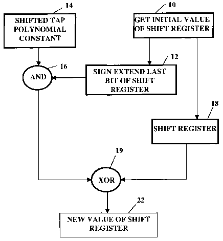
Figure 2 shows the technique of the preferred
embodiment.
It will be appreciated that the tap polynomial
for either the long or short code can be represented as a
binary sequence. This needs to be combined with the
current value of the shift register in order to obtain the
new value of the shift register.
In the first preferred embodiment, the tap
polynomial binary sequence is shifted one bit towards the
most significant bit and the least significant bit is set
to have the value 1. This produces a shifted tap
polynomial constant which is stored in a data entity as
indicated by step 14. The method then involves getting
initial or current value of the shift register at step 10
and extending the last bit of the shift register to have
sufficient bits in order for it to be combined with the
shifted tap polynomial constant. At step 16 an AND
operation is performed on the shifted tap polynomial
constant using the sign extended last bit of the shift
register. At step 18 the current value of the shift
register is shifted by one bit towards the most
CA 02429080 2003-05-15
WO 02/41512 PCT/AU01/01405
- 11 -
significant bit. This shifted register is then combined
at step 19 with the result of the AND operation performed
at step 16 by performing an XOR operation. The result of
the XOR operation then implicitly provides the new value
of the shift register which can then be used to generate a
further bit of long or short code.
Figure 2 shows a slightly less efficient
technique of a second less preferred embodiment. In this
embodiment an unshifted tap polynomial constant is used as
indicated at step 35. At step 30 the initial value of the
shift register is obtained and the last bit of the shift
register is sign extended. At the same time, the value of
the last bit is saved at step 32. The sign extended last
bit of the shift register is combined with the tap
polynomial constant at step 38 using an AND operation and
the result of this AND operation is combined with the
initial value of the shift register using XOR operation at
step 40. Following the XOR operation the result of the
XOR operation is shifted towards the most significant bit
and the saved value of the last bit from step 32 is loaded
into the least significant bit at step 44 to produce the
new value of the register at step 46.
Example 1 - Long Code
Following, the calculation of a chip of long code
it is necessary to quickly update the shift register so
that the next chip can be generated.
The Binary sequence that represents the long code
tap polynomial p(x)= X42 + X35 + X33 + X31 + X27 + X26 + X25 + x22
+ X21 -I- X19 -i- X18 f X17 -I- X16 i- x10 -I- X7 -i- X6 _i- XS -1- X3 f X2 .I-
Xl -I-
1 is given by
100000010101000111001101111000001001110111
CA 02429080 2003-05-15
WO 02/41512 PCT/AU01/01405
- 12 -
with the MSB is on the left and the LSB is on the
right.
Shifting the register prior to applying the tap
polynomial provides the most efficient technique for
updating the shift register holding the long code. Bit O
of the shifted version of tap polynomial is assigned the
value 1. The shifted tap polynomial has the following
form:
000000101010001110011011110000010011101111
The value of the last stage of the shift-register
is saved and sign extended to have the same number of bits
as the long code tap polynomial as indicated by step 12 of
Figure 2.. Then an AND operation is performed with the
shifted tap polynomial. The first stage of the register
will be loaded with the desired value automatically
without any explicit operation.
Assume that 42-bit data is representing the
current state of the long code sequence stored in two 32-
bit data entities, and is for example:
Bit 31 Bit 0
0110 1110 1010 0000 0100 0111 0110 0101
Bit 63 Bit 32
0000 0000 0000 0000 0000 0011 0001 1101
Note that bits 42-63 are allocated the value 0.
The fast shift register update is then carried out as
follows:
The shifted version of the tap polynomial is stored in two
32-bit entities as:
CA 02429080 2003-05-15
WO 02/41512 PCT/AU01/01405
- 13 -
Bit 31 Bit 0
1000 1110 0110 1111 0000 0100 1110 1111
Bit 63 Bit 32
0000 0000 0000 0000 0000 0000 0000 1010
This represents the actual polynomial for CDMA systems
shifted by one bit with Bit 0 set to 1.
Last stage of the shift register (Bit 41) is 1. Sign
extending it to 32-bits gives:
1111 1111 1111 1111 1111 1111 1111 1111
This is saved. If a 64-bit data entity Were used, the
last stage would need to be sign extended to 64-bits.
That is, in the 32-bit case the data entity holding the
extended last stage can be used to perform the AND
operation on both the entities in which the polynomial is
stored.
Now we shift the shift register left by one bit.
Result is:
Bit 31 Bit 0
1101 1101 0100 0000 1000 1110 1100 1010
Bit 63 Bit 32
0000 0000 0000 0000 0000 0010 0011 1000
Note that as we are representing a 42-bit register, bits
42 to 63 are always assigned the value "0".
Logically AND-ing both 32-bit entities of polynomial with
the saved value of the sign-extended last stage gives the
polynomial result:
CA 02429080 2003-05-15
WO 02/41512 PCT/AU01/01405
- 14 -
Bit 31 Bit 0
1000 1110 0110 1111 0000 0100 1110 1111
Bit 63 Bit 32
0000 0000 0000 0000 0000 0000 0000 1010
Logically XOR-ing those values with the shifted shift
register produces the result:
1101 1101 0100 0000 1000 1110 1100 1010 XOR (Shift
Register value bits 0-31)
1000 1110 0110 1111 0000 0100 1110 1111 (Polynomial result
bits 0-31)
Results:
Bit 31 Bit 0
0101 0011 0010 1111 1000 1010 0010 0101 (New value of
shift register, bits 0-31)
0000 0000 0000 0000 0000 0010 0011 1000 XOR (Shift
Register value bits 32-63)
0000 0000 0000 0000 0000 0000 0000 1010 (Polynomial bits
32-63)
Equal to:
Bit 63 Bit 32
0000 0000 0000 0000 0000 0010 0011 0010 (New value of
shift register, bits 32-63)
New value of shift register is:
Bit 31 Bit 0
CA 02429080 2003-05-15
WO 02/41512 PCT/AU01/01405
- 15 -
0101 0011 0010 1111 1000 1010 0010 0101
Bit 63 Bit 32
0000 0000 0000 0000 0000 0010 0011 0010
In the second preferred embodiment all stages of
the shift register that correspond to a polynomial tap are
XOR-ed with the value of the last stage, the shift
register is then shifted and the value of the last stage
is fed into the first stage of the shift register. The
desired effect is obtained by converting the tap
polynomial into a 42-bit binary sequence, then AND-ing
every bit of it with the output from last stage of the
shift register, and finally XOR-ing the result with
current state of the shift register. Once this operation
is complete, the contents of the entire shift register are
shifted once and the saved value of the last stage is
moved into the first stage.
Example 2 - Short Code
The shifting of the short code register occurs
1536 times for every power control group (PCG), with both
the I and Q shift registers requiring this operation. The
tap polynomials for the Short Code shift registers are:
,PI (X~ - X15 f X13 f ~ f X8 -I- X~ f XS -I~ .1
,PQ ~X~ . X15 f X12 -f. Xll .l- Xl~ ~. X6 f X5 t X4 f X3 ~I- Z
The shift registers for the I and the Q branches
are represented by 16-bit data entities. Thus, both shift
registers will occupy only 32 bits of memory.
The register is shifted prior to applying the tap
polynomial. The tap polynomial is also shifted with the
first bit set to 1. The shifted tap polynomials have the
following forms
CA 02429080 2003-05-15
WO 02/41512 PCT/AU01/01405
- 16 -
0010 0011 1010 0001 (I-seguence, listed from left to right
in the order MSB to LSB)
0001 1100 0111 1001 (Q-seguence, listed from left to right
in the order MSB to LSB)
It will be noted that bit 15 has been set to zero.
The shifted tap polynomials are then logically
AND-ed with the extended value of the last stage of the
shift register before the result is logically XOR-ed with
the shifted shift register.
In the alternative, the tap polynomial is
converted into a 15-bit binary sequence. This sequence is
logically AND-ed with the output from the last stage of
the register and XOR the result with current value of
shift register. After that shift register is shifted one
bit towards the most significant bit and the value of the
last stage is fed into the first stage.
In this case the unshifted binary sequences that
represent the tap polynomials are:
0101 0001 1101 0000 (1-sequence, Iisted from left to
right in the order MSB to LSB)
0100 1110 0011 1100 (Q- sequence, listed from
left to right in the order MSB to LSB)
It will be noted that bit 15 has been set to zero.
Instead of AND-ing every bit of the tap
polynomial sequence with the value of the last stage of
the register (which requires 15 shifts and 15 AND
operations), the value of the last shift register stage is
first extended to the full 15 bits (actually to 16 bits in
a C language implementation, where the shift register is
physically represented by a 16 bit data entity). We then
make use of signed arithmetic and shift this value left to
the MSB position and shift it back to the LS8 position to
CA 02429080 2003-05-15
WO 02/41512 PCT/AU01/01405
- 17 -
sign extend the value to the full 16 bits.
The value of the last stage is saved and sign-
extended to 16-bits. The AND and XOR operation can now be
accomplished easily and the register is shifted one bit
towards the most significant bit. Finally the previous
value of the last stage of shift register is assigned to
the first stage.
It will also be apparent that skilled programmers
can generate an appropriate computer program for
implementing the method of the invention. The invention
includes within its scope such a program and a processor,
such as a DSP, so programmed.
Various modifications to the foregoing system
will be apparent to persons skilled in the art and should
be considered as falling within the scope of the present
invention.