Note: Descriptions are shown in the official language in which they were submitted.
CA 02430741 2003-06-05
WO 02/49199 PCT/GBO1/05349
ELECTROSTATIC DE'~ICE
The present invention relates to electrostatic devices, in particular
actuators and
sensors of the type commonly referred to as Micro-Electro-Mechanical Systems
(MEMS)
or micromachined devices.
Generally, prior art electrostatic transducer devices, whether actuators or
sensors,
comprise first and second members connected to a drive voltage-source. The
resulting
attractive electrostatic forces cause at least one of the members to move
towards the other.
For this purpose, the members are normally made of conductive material, such
as metals
and doped-polysilicon to facilitate charging and discharging and ensure proper
operation.
Prior art devices are disclosed, for example, in the "Micromachined
Transducers
l0 Sourcebook"by G.T.A. Kovacs, WCB/McGraw-Hill, 1998, at pages 278 to 281,
such as
the classic cantilever actuator having a movable electrode suspended above a
stationary
counter-electrode by a gap. This suffers from the inextricable link between
the gap length
and useful deflection, with the latter usually much less than but not
exceeding. the gap
itself. Larger deflections require larger gaps and consequential large
voltages that are very
15 often incompatible with standard IC drive electronics. For many
applications it is highly
desirable to make devices having deflections larger than the actual gap. This
book
discloses a comb-drives actuator which has a large number of fine
interdigitated forgers
producing attractive forces mainly due to fringing fields, which can produce
larger
movements inherently in the substrate plane. Comb-drive actuators suffer from
several
2o problems including: relatively large support/springs passive area, limited
out-of plane
movement, difficulty in maintaining the desirable centrally-balanced f nger
positions,
particularly at smaller gap widths.
Other prior art includes the article "Distributed Electrostatic Micro
Actuator" by
Motoharu Yamagauchi et al of Tohoku University published by IEEE in 1993, and
United
25 States patent no. 5,206,557. Both documents provide large number of members
connected
in series to produce larger in-plane strokes that are not inherently capable
of out-of plane
motions. The stacked members effectively form long chains with normal pulling
forces.
Together with comb-drives, manufacture of these devices is compounded by the
requirement to micromachine deep structures with narrow gaps, a difficult task
likely to
30 cause trade-off between achievable gap widths and drive voltage levels (and
performance).
This reduces compatibility with standard integrated circuit drive voltage
levels and
manufacturing.
W--- . ._...r... ~ v.
r.'C~a~''~ .. ~ ; ' ~ "tea '.es;~f w ~~,~c'e "~a x ' v:':
s ~°,i'fi' : ~ "u.~ r.
la
US-A- 5,793,560 discloses a storage device which includes a substrate, a
magnetic
storage medium provided on the substrate, information being magnetically
stored in the
magnetic storage medium, a head unit; and a reciprocating mechanism provided
on the
substrata, tfie reciprocating mechanism causing the head unit to reciprocate
in a plants
parallel to a surface of the magnetic storage medium, wherein, while the head
unit is being
moved by the reciprocating mechanism, information is.recorded in or reproduced
from tlac
magnetic storage maiium view the head unit.
US-A- S 64~ O1 S discloses an electromechanical transducer having a substrate
bearing a plurality of elastomeric rnicrostractures with a microelectmde on
each
microstructure. A power supply is cc~nnccted to the znicroelectxodes for
controlled
application to tbem of an electrical p~~tcntial which alternatively induces
forces of
attraction between adjacent pairs ofrnicroelectrodes, causing controlled, timo-
varying
displacement of the microelectrodes.
US-A-S 479 0G1 discloses an electrically and mechanically robust
microelextromechanical transducer formed of a pleated dielectric sh having
paxterned
electrical conductors on the opposin;~ faces thereof. 'fhs pleats define a
plurality of spaced
apart walls, with each wall including an electrically conductive portion at
one side thereof:
Positive and negative voltages, applied to opposite faces of the pleaxe sheet,
cause the
walls to move towards one another try electrostatic attraetion_ 'The w s can
also move
away from oz~e another by elecfiostatic repulsion upon application of ~mpriate
voltages_
Emvfanssteil l4.Mart 18:35 ~~ '
~-° CA 02430741 2003-06-05
CA 02430741 2003-06-05
WO 02/49199 PCT/GBO1/05349
The present invention seeks to provide improved electrostatic devices.
According to an aspect of the present invention, there is provided an
electrostatic
device including a first flexible electrode able to be deflected and at least
one second
electrode mounted on the first electrode so as to move therewith and to cause
deflection of
the first electrode upon the application of an electrical charge to the
electrodes.
The or each second electrode works to create enhanced deflection of the first
electrode upon the establishment of an electrostatic force as it moves with
the first
electrode. The maintenance of close proximity of the first and second
electrodes allows
higher electrostatic forces, power density, efficiency to be developed andlor
lower
l0 operating voltages which can be maintained even at large deflections. The
device can
operate at drive voltage levels compatible with semiconductor integrated
circuits. It can
also actively transform the high force/low deflection exhibited by the prior
art devices to a
lower force and larger deflection (and vice versa), in effect providing built-
in mechanical
magnification, improving load adaptability. Moreover, the inextricable link
between
is inter-electrode gap and deflection in prior art devices can be successfully
de-coupled,
allowing each to be advantageously optimised separately.
Design flexibility can be facilitated by using the number of cells N as an
additional parameter for increasing deflection, and/or for trade-off between
deflection and
force, and vice versa. For example, if a smaller gap is used (for example, for
reasons of
20 one or more of lower drive voltage, higher power density and efficiency),
deflection may
still be enhanced by increasing N.
Devices made by the teachings herein may provide relatively large out-of plane
as
well as in-plane movements and deflections.
Thus, the amount of movement of the first electrode per unit of applied
voltage is
2s increased compared to prior art devices. This can enable the device to be
operated at Iower
voltages, even voltages typically used in integrated circuits (ICs). Thus, as
well as
compatibility with IC fabrication, the devices may be integrated with ICs and
drive
electronics (e.g. monolithically) leading to significant cost reductions.
For many applications it is highly desirable to make devices having large
3o deflections while keeping the gap small. Furthermore, smaller gaps lead to
the advantage
of higher power densities, efficiencies and/or lower drive voltage levels.
CA 02430741 2003-06-05
WO 02/49199 PCT/GBO1/05349
In the preferred embodiment, there is provided a plurality of second
electrodes
located proximate one another on the first electrode. A plurality of second
electrodes
increases the deflection of the first electrode.
Where a plurality of second electrodes is provided, these may be arranged in a
linear array or may be in any other arrangement. Where they are arranged in a
non-linear
array, they can produce deflections of the first electrode about more than one
axis to create
complex actuator or sensor movements.
In an embodiment, there is provided a plurality of second electrodes arranged
on
the first electrode or electrodes to provide movement of the first electrode
or electrodes in
opposing directions. In one example, one or more second electrodes may be
located in
what could be termed on the top surface of the first electrode and one or more
second
electrodes located in what could be termed on the bottom surface of the first
electrode;
such that the top second electrodes) produce a downward deflection or movement
of the
first electrode and the bottom second electrodes) produce an upward deflection
of the first
electrode.
Where a plurality of second electrodes is provided, these may overlap, for
example by the provision of fingers which interdigitate with the fingers of
the other
electrode. Alternatively, adjacent rows may be staggered to effect another
form of overlap.
Preferably, there is provided a common supply rail for supplying the or a
plurality
of second electrodes with power. Where there is provided a plurality of second
electrodes
to be driven in different manner, a plurality of supply rails may be provided.
The gap between the first and second electrodes may be kept under a vacuum or
filled with one or more of a gas, liquid, gel or deformable solid material.
The first and/or second electrode or electrodes may have access holes for
manufacturing purposes or other apertures, weakness or strengthening areas to
adjust the
deflection thereof. Alternatively, the first electrode may have no holes for
applications as
pumps and pressure sensors.
The first andlor second electrodes may be in the form of layered members
including at least one conductive layer.
3o According to another aspect of the present invention, there is provided an
electrostatic device including first and second electrodes arranged in first
and second
CA 02430741 2003-06-05
WO 02/49199 PCT/GBO1/05349
4
planes respectively, both of which electrodes are operable to move in a
direction at an
angle to the plane thereof on application of an electrical charge between the
electrodes.
According to another aspect of the present invention, there is provided an
electrostatic device produced by an integrated circuit or a
micromachining/MEMS
fabrication technique.
The invention also extends to actuators and sensors and devices incorporating
actuators and sensors which use an electrostatic device, as taught herein.
It is possible with the present invention to provide new types of actuators
and
sensors which can be operated at lower voltages making them more compatible
with
l0 integrated circuits. The actuators can have improved deflection versus
vo1_tage
characteristics and improved trade-off between deflection and force, and more
sensitive
sensors.
Furthermore, the present invention can offer more versatile and flexible
actuator
design parameters. It can provide devices which are capable of motions and
deflections in
15 and out of their own planes, thereby moving in three axes.
Embodiments of the present invention are described below, by way of example
only, with reference to the accompanying drawings, in which:
Figures 1, 2a and Zb show plan and side elevational views of an embodiment of
electrostatic actuator;
2o ' Figures 3a and 3b are side elevational views of another embodiment of
actuator,
with Figure 3b showing the actuator in a deflected position;
Figures 4 and 5 are, respectively, plan and side elevational views of another
embodiment of electrostatic actuator;
Figures 6 to 8 are side elevational view of three different embodiments of
actuator
25 able to deflect in two opposite directions relative to a rest position;
Figures 9 and 10 show views of two embodiments of actuator with a plurality of
second electrodes in a linear array;
Figure 11 shows another embodiment of complex electrostatic device;
Figures 12a to 13b are plan views of two different embodiments of actuator
able
3o to deflect about two different axes;
Figures 14 to 16 show different embodiments of complex electrostatic device;
Figures 17 to 24 show different embodiments of actuator or sensor;
CA 02430741 2003-06-05
WO 02/49199 PCT/GBO1/05349
Figures 25A to 26C show examples of connection between supply rail and the
electrodes;
Figures 27A to 27E show different embodiments of bridge supports;
5 Figures 28 to 29 show different examples of connection between a first
conductor
and a second conductor; and
Figures 30A to 30C show an embodiment of method of manufacture of an
actuator as herein described.
It will be apparent to the skilled person that the actuators described herein
could
l0 also be used as sensors and therefore the term "device" is intended to
encompass both
actuators and sensors. Furthermore, on the whole the description focuses on
actuators for
simplicity only and it is intended that equivalent sensors are also
encompassed.
In this specification, electrode E1 refers to members l, 31, 91 and 101
described
below, and electrode E2 refers to members 2, 32, 92 and 102 described below.
Devices
able to deflect or bend about one or more axes may be referred to herein as
single axis
devices, double axis devices and so on.
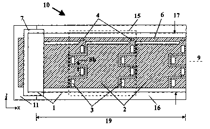
Referring to Figures l, 2a and 2b the embodiment of device shown can deflect
about one axis (in this example about the Z-axis). Figure 1 shows the device
in plan view,
while Figure 2a shows a side elevational view of the device. For ease of
understanding,
Figure 1 shows the first layer in outline only, but is shown in solid form in
Figures 2a and
2b.
The device 10 comprises an electrically conductive first member or layer 1 of
stiffness k1 and an electrically conductive second member or layer 2 of
stiffness k2
separated from one another by an electrically insulating layer,3 which
provides a
separation gap 3a between members 1 and 2. The members l, 2 form first and
second
electrodes E1, E2 of the device respectively. Layer 3 provides support posts
or anchor
pads also acting as spacers maintaining gap 3a between the members 1 and 2.
The members 1 and 2 and the layer 3 form a plurality of bridge-like cells 15.
An
array of these cells 15 share a common first member 1 (electrode El) and
together form a
3o flexible structure 18 which forms the main body of the device.
The member 18, which has an active length 19 and width 17, is mounted and
fixed to a support post 11 raised above substrate 16 by gap 14. Thus, the
member 18 is
CA 02430741 2003-06-05
WO 02/49199 PCT/GBO1/05349
6
suspended above the substrate 16 and its free (cantilevered) end can move
along angular
direction 12 shown in Figure 2b.
The first member 1 may be substantially continuous throughout the cells 15
while
member 2 is segmented to form a plurality of individual cells 1 S. The cells
15 may have
any appropriate length and dimensions and may be repeated further along
direction 9
and/or laterally along the Z axis.
In the embodiment of Figures 1, 2a and 2b, the second members 2 (electrodes
E2)
are provided with a plurality of fingers which extend in the plane of the
member and are
arranged such that the fingers of adjacent members 2 interdigitate. This
improves the
to deflection of the first member 1, as is described below. In this
embodiment, adjacent
members 2 are separated by gap 8b and overlap one another by distance 8a.
Distance 8a
may be of any desirable value and is preferably less than half a cell-length.
Figure 2b shows the device 10 in the deflected state.
The electrical connection terminals for the members 1 and 2 (electrodes El and
15 E2) are at location 11 to facilitate connection to voltage or power supply
5. Each second
electrode E2 is connected to a common supply rail 6 which may be formed from
the same
layer.
Since electrode E1 is shared between the cells 15, its end is available at
location
11 for connection to power supply 5.
2o Like electrode E2, member 6 may also be separated from electrode E1 (if
they
overlap) by anchor pads 4, similar to 3.
The mechanical properties, such as stiffness (k) and thickness (t), of the
various
members, the length-19 of the device 10, the length of the cells 15, the
active cell
bridge-length (that is between members 3) and width 17 and other relevant
parameters may
25 be appropriately chosen for the particular application under consideration
and to achieve
operating characteristics desired. In common with most electrostatic devices,
the energy,
force and power are generally proportional to~the device's active area and the
electric field
between electrodes El and E2. The force may be increased by increasing the
active area,
such as by increasing the cell's width 17 andlor using parallel rows of cells.
Moreover, the
3o power density (and force) may be increased by increasing the electric field
or if the desired
voltage level is fixed, the inter-electrode gap may be reduced. The number of
cells along
CA 02430741 2003-06-05
WO 02/49199 PCT/GBO1/05349
7
length 19 may then be appropriately chosen in order to produce the desired
deflection
magnitude, using the built-in magnification capability of the device.
One example may have N=10-20 and approximate dimensions of: tlpayer y=1
micrometre, t2(layer 2) '2 micrometres and t3yaYer 3)=1 micrometre, these
dimensions of
course being dependant upon desired performance and other requirements.
When the device 10 is connected to voltage source 5, electric/electrostatic
charges
accumulate as a result of capacitance between electrodes E1 and E2, giving
rise to
attractive electrostatic forces between the electrodes E1 and E2. This causes
electrode El
to deform or curl and its free end to deflect out-of plane along angular
direction 12 as
shown in Figure 2b. The deflection magnitude is praportional to the level of
applied
voltage. The deflection direction is from the second electrodes to the first
electrode. It can
also be seen that the device's effective length along the X-axis reduces to
19a as a result of
contraction by an amount 19b (explained in more detail below).
Disconnecting the power supply 5 will keep the device in its deflected state
for a
period of time depending on the level of electrical insulation between
electrodes El and
E2. To return the device 10 to its undeflected state, the electric charges
need to be
removed, for example by shorting electrodes E1 and E2 together in order fox
the entire
structure 18 to spring back.
The total end-deflection D at 12 is the sum of the deflection caused by each
individual cell 15. More specifically, each cell 15 contributes a fraction
towards the total
deflection D of electrode El, and the larger the number of cells 15 the larger
is the overall
deflection D and length contraction 19b. This will become apparent from a
consideration
of Figure 3b.
The bending magnitude depends on cell dimensions, location within the device
and may further depend on load type and condition. The device 10 may produce a
number
of motions and forces depending on the method of mounting and/or clamping
used. For
example, clamping at the centre will cause the ends to deflect angularly
upwards while
clamping the ends will cause the centre to move downwards in a translational
or linear
fashion along the Y-axis. By placing electrodes E2 on the opposite side of El,
the device
will deflect in the opposite direction.
Among the main general features of the device 10 are the following. Unlike the
prior art, the devices have high energy density and capability by maintaining
close .
CA 02430741 2003-06-05
WO 02/49199 PCT/GBO1/05349
8
proximity between electrodes E1 and E2 and the resulting high electric field
levels. It
provides unique flexibility with which the number of cells N can control the
trade-off
between deflection D, force F, among other variables. Generally, for a given
device 10
increasing N can increase D at the expense of F and vice versa. Many prior art
devices are
generally forced to use high drive voltages often well beyond the desirable
levels used in
semiconductor integrated circuits. On the other hand, the device 10 can
actively transform
the high force and low relative displacement between members E1, E2 to a lower
overall
force F and larger overall deflection D, providing in effect mechanical
magnification (and
vice versa), using lower V levels.
l0 Figures 3a and 3b show another embodiment of device 20 in ~~~hich the
second
electrodes E2 do not interdigitate or otherwise overlap. Rather, these
electrodes E2 are
rectangular in shape and are spaced from one another by a gap 8c. If desired,
an
overlapping version of device 20 may be made using a number of rows of
electrodes E2
with the positions of adjacent rows shifted (along the X-axis) relative to one
another.
15 As can be seen in Figure 3b, the deflection caused to the first electrode
E1 extends
over its entire length as a result of the bias to deflection caused by its
major portions being
deflected by the second electrodes E2. Figure 3b also shows the upward
deflection of the
first electrode El, in practice in a direction opposite the second electrodes
E2.
Figures 4 and 5 show another embodiment of device 30 which deflects about a
20 single axis (in this example the Z-axis). In this embodiment, the second
electrodes 32 are
of a cantilever type, being connected only at one end to the first electrode
31.
This device 30 comprises an electrically conductive first member 31 (forming
electrode El) of stiffness k31, electrically-conductive second members 32
(forming
electrodes E2) of stiffness k32, separated by an electrically-insulating layer
33 providing a
25 separation gap 33a between the members 31 and 32. The member 31 and each
member 32
with support layer 33 form a cantilever-like cell 45. It is not necessary for
the support
layer 33 to be located at one end of the second member 32 as it can also be
located
elsewhere, for example at its centre to provide two cantilevered sides sharing
common
anchor pad.
30 As with the embodiment of Figures 1 to 3b, an array of one or more cells 45
sharing a common first member 31 forms a flexible structure which provides the
main
body of the device 30. This flexible structure, with active length 39 and
width 37, is
CA 02430741 2003-06-05
WO 02/49199 PCT/GBO1/05349
9
mounted and fixed to support post 41 raised above substrate 46 by gap 44 and
free to move
out-of plane along angular direction 42. The cells 45 may have any appropriate
length and
dimensions and may be repeated along direction 39a if desired.
Members 32 of adjacent cells are separated by gap 49.
Insulating landing pads 48 may be'used to prevent members 31 and 32 from
coming into contact with one another during deflection. The pads 48 may also
have other
functional purposes: for example, they can cause the second electrode E2 to
change from
being of a cantilever type to a bridge type upon contact with its pad or pads
48 and thus
alter the type of deflection imparted to the first electrode El. This could be
useful as a
l0 limit switch or sensor.
As with the previous embodiments, members 32 are connected to supply layer 36
which may be formed from the same layer as the members 32. The first member 31
can
extend to location 41 where it connects to power supply 35. Like members 32,
member 36
may be separated from the first member 3 I (if overlapping) by anchor pads and
insulating
15 spacers 33.
All members 31, 32, 33 may be made of any appropriate material.
The mechanical properties and dimensions, such as stiffness (k) and thickness
(t),
of the various members 31,32, the active length 39 of the device, the
cantilever-length and
the active length of a cell, that is between members 33 and width 37, among
other relevant
20 parameters, may be chosen in dependence upon application. Members 32 of
adjacent cells
in 30 can also overlap if desired.
When the device 30 is connected to voltage source 35, electric/electrostatic
charges accumulating on the members 31,32 will deform member 31 along angular
direction 42 from member 31 to members 32. Device 30 also undergoes length
contraction
25 similar to 19b of device 10 in Figure 2b.
A cantilever-type device 30 deflects in an opposite direction to a bridge type
device and, depending on the type of mounting and/or clamp used, may deflect
in a
number of ways similar but opposite to a bridge-type device. The bending
magnitude
depends on cell dimensions and location within the device, and may also depend
on load
30 type and condition. Cantilever devices generally have similar features to
the bridge
devices.
CA 02430741 2003-06-05
WO 02/49199 PCT/GBO1/05349
It will be apparent that bridge and cantilever types can be provided in the
same
device and indeed on the same first electrode El.
Figures 6 to 8 show examples of bi-directional devices. Bi-directional devices
may be made using a double-sided arrangement of second members 2, 32 sharing
one
common member 1, 31 (respectively) in back-to-back fashion. For example, each
device
may have its independent electrical connection while sharing one of electrodes
E1 or E2 as
a common member and terminal, such that each can be turned on/off
independently.
One such embodiment is shown in Figure 6, which comprises two sets of second
electrodes E2 and one common electrode El sandwiched between the two sets of
second
l0 electrodes E2 of the bridge type. In effect, this sandwich arrangement
form__s two devices
sharing one common electrode El capable of producing deflections in either
direction
along arc 89 while the other end of the device is fixed at 85. The device 40
(alternatively
clamped via electrode El alone) deflects up and down if the bottom or top sets
of
electrodes, respectively, are actuated independently. Alternatively, two
single direction
devices may be coupled such that each may deflect the combined device in a
separate
direction.
Anchor pads 3 in the top and bottom sets of second electrodes E2 may be in
alignment with each other and may have the same positions in the XZ-plane.
Other bi-directional devices may be made using only two electrodes E1 and E2
(instead of the three electrodes E2, El, E2 as in device 40 of Figure 6) as
shown in Figures
7 and 8. These can use a commonly available standard fabrication process
requiring only
two conductive layers and one insulating layer, for example by a two
structural polysilicon
layer process. This flexibility alloys the fabrication of different types of
devices, for
example some bi-directional, some upward-deflecting single-direction, some
downward
deflecting single-direction or a combination of these, all using the same
fabrication run or
batch and/or the same substrate. Thus, one can advantageously make bridge and
cantilever
devices and/or devices combining both types, capable of deflecting in any
single or
bi-directional manner.
Figure 7 shows an example of two layer bridge-type bi-directional device fixed
to
support post 71 comprising an insulating anchor pad layer 73, conductive
layers 74, 75
joined at point 76. For example, an upward-deflectable part 77 can be made on
the left side
by making or configuring layer 74 as the second electrode E2 and layer 75 as
the first
CA 02430741 2003-06-05
WO 02/49199 PCT/GBO1/05349
11
electrode El, and a downward-deflectable part 78 can be made on the right side
by malting
layer 74 as the first electrode E1 and layer 75 as the second electrode E2. A
substantially
continuous first electrode El is formed by joining members 74 and 75 at
position 76. The
parts 77, 78 may have one or more independent and/or shared electrical
tenninal(s), and
may be repeated along 79 (or other rows as in Figure 11) to make a device of
any desirable
size and deflection characteristics.
It is not necessary that just the first electrodes are coupled together. An
alternative is to connect electrode E1 of one device to electrode E2 of
another device or to
any other moveable part thereof.
l0 Figure 8 shows another embodiment of bi-directional device having both
bridge
and cantilever types of cell and fixed at support post 81. The device
comprises an
insulating anchor pad 83 and conductive layers 84 and 85. For example, an
upwardly
deflectable bridge part 87 can be made on the left-hand side by making layer
84 as
electrode E2 and layer 85 as electrode El; while a downwardly deflectable
cantilever part
88 can be made on the right-hand side by making layer 84 as electrode E2 and
layer 85 as
electrode E1. The combined parts 87, 88 may have one or more independent
and/or shared
electrical terminals) and may be repeated along 89 (andlor in other rows as in
Figure 11)
to make a device of any desired size and deflection characteristics.
Advantages include:
both bridge and cantilever cells use the same material/layer for electrode E1,
and the same
2o material/layer for electrodes E2; El and E2 are located on the same side of
the device,
which may be desirable in some applications.
Although layers 74, 75 (84, 85) may be configured as electrodes E1 or E2 or
both,
their thicknesses, however, are usually axed and not readily controllable in a
standard
MEMS fabrication process. Thus, if desired and in order to optimise layers
74,75 (or
84,85) to function as E1 or E2 or both, their effective stiffness (k) may be
controlled by
varying the effective width of members E1, E2, for example by making holes or
slits along
the width to reduce k1, k2 (stiffness of electrodes El and E2 respectively).
Electrode
connections for Figure 7, 8 may be of any appropriate type, e.g. as shown in
Figures
25A-29. This technique may also be used to make up/down devices in the same
3o fabrication process.
Parts 77, 78, 87 and 88 may each comprise one or more cells.
CA 02430741 2003-06-05
WO 02/49199 PCT/GBO1/05349
12
Any appropriate cell form, shape, dimension, number of overlapping parts of
angers may be used. Further examples are shown in Figures 9 and 10, in which a
plurality
of cells formed by members El, E2 and 3 equivalent to those of the bridge
device 10 with
electrodes E2 overlapping by distance 8a. Electrode E1 is shown in an outline
form solely
for the purposes of illustration. The cell shape is not fixed and can be of
any shape to
produce or promote particular deflections. They could, for example, be
rectangular,
square, triangular, polygonal or of chevron shape. Similarly, any appropriate
electrical
connection (not shown) may be used, including connections of the type shown in
Figures
25A to 29.
l0 In addition to being able to provide devices having a single row of cells,
it is
possible to provide devices having a plurality of such rows, one device being
device 170 of
Figure 11. A common first electrode El may be shared by the rows. The adjacent
rows
may stagger relative to one another to overlap. The rows may deflect in the
same or in
different directions and may be independently controllable if desired.
Devices Deflectable about two Axes
Figures 12a to 13b show examples of devices which are capable of deflecting
about two axes on the establishment of an electrostatic force between members
El and E2,
for example about the Z-axis and about the X-axis or having deflection
components about
2o these axes. In general terms, members 91 and 101 in Figures 12a and 13a axe
the flexible
electrodes E 1 (shown in outline form only for ease of understanding) and
could be
considered similar to a flexible diaphragm.
Figures 12a shows an example of a device 90, which can be considered similar
to
a bridge-type device (such as device 10 of Figure 1). Device 90 comprises
members 91
and 92 (in this example there being three members 92) similar to members 1 and
2 of the
device 10 of Figure 1, respectively. For this purpose, members 92 have an
appropriate
shape, in this example hexagonal, which may also have fingers (not shown)
around the
edges which interdigitate with its neighbours at region 98 as with the
embodiment of
Figure 1. The members 92 are separate from one another and are supported on
member 91
(in this example behind 91) in a manner similar to that of a bridge-type
device via similar
anchor pads, for example one or more per finger.
CA 02430741 2003-06-05
WO 02/49199 PCT/GBO1/05349
13
Alternatively, members 92 may be spaced out from one another by gaps similar
to
the embodiment of Figures 3a and 3b. Only three cells are shown in the
embodiments of
Figures 12a and 13a but more may be added along lines 99 and 109;
respectively, in order
to make arrays of any desired size, deflection and number of cells (similar to
that of Figure
24).
Instead of interdigitated fingers, members 92 may have any appropriate shape
and
are supported by anchor pads placed at appropriate positions such as near some
or all the
corners or vertices of members 92 in order to facilitate bending about two
axes.
Furthermore, members 92 in adjacent cells may have any desired form and degree
of
l0 overlap to enhance device performance. An alternative form of members 92 is
shown in
Figure 12b, each comprising four forgers which mesh or interdigitate with
members 92 of
its adjacent-cells, and providing cell overlap along two axes.
If the member 91 is fixed at its periphery, upon actuation it will deform
about the
X and the Z-axes forming a curved surface with electrodes E1 and E2 located at
the
concave and convex surfaces, respectively. Alternatively, any other fixing
method,may be
used, such as at the centre. Among some of its applications, the device 90 may
be used in
MEMS micro-speakers, microphones, micro-pumps, inkjet pumps and so on.
Figures 13a shows an example of a device 100 which can be considered similar
to
a cantilever-type device, comprising members 101 (as E1), 102 (as E2) and 103.
Members
102 are supported, such as at their centres, on members 101 via anchor pads at
appropriate
positions 103. In this example, both members 101 and 103 may be placed behind
members
102 (103 are shown in front of 102 in Figure 13a only for ease of
understanding) so that
device 100 can deflect in a similar direction to that of device 30. For
example, if member
101 is fixed at its periphery, then upon actuation it will deform about the X
and the Z-axes
forming a curved surface with electrodes E2 and E1 located at the concave and
convex
surfaces, respectively. This type of deflection is shown in Figure 13b, which
uses
square-shaped electrodes E2 and E1 with electrode E1 fixed at its corners (and
it will be
apparent that the embodiments of Figures 12a and 12b will deflect in like
manner).
The cells may overlap if desired.
As with device 90, the region between adjacent cells in device 100 may contain
one or more electrical interconnections, for example connections 108, as
described herein.
Similarly, the second members 92 or 102 (constituting the second electrodes
E2) could be
CA 02430741 2003-06-05
WO 02/49199 PCT/GBO1/05349
14
powered together or separately in dependence upon application. Device 100 has
similax
applications to that of device 90.
Only three cells axe shown but more cells may be added along lines 109 to make
an array of any desired size and number of cells. Similarly, the devices 90
and 100 and
electrodes 91, 101 may have any desirable and appropriate shapes, for example
hexagonal
(as in Fig. 24) circular, square, even non-symmetrical.
A bi-directional device deflectable about two axes may also be made by
duplicating members 92,93 on the other side of member 91 in device 90, and
duplicating
members 102, 103 on the other side of member 101 in device 100.
The skilled person will recognise that techniques similar to that used in
Figures 7
and 8 may also be used to make double axis devices of the bridge-like,
cantilever-like or a
combination of both in the same device, which are capable of deflecting in a
single or
bi-directional manners using a two structural electrodes fabrication process.
Other embodiments which can move about two axes may be made by using two
devices which each move about a single axis coupled to one another at an
angle. They
may be provided with shared or independent terminals for control. For example,
device
140 of Figure 14 may be modified to make a device movable about two axes by
orienting
one or more rows at 90° to one or more other rows in the same device.
Upon actuation,
each device will cause deflection about one axis. Device 180 shows another
example
which can also deflect about two axes. Electrodes E1 may have slits, apertures
or holes to
further promote or enhance operation.
Complex Devices
It is also possible to create complex devices formed of a plurality of sets of
second
electrodes either on a single first electrode or on a plurality of first
electrodes. In the
former case, the first electrode can be made to deform in complex manners to
provide
complex types of movement of one or more device attached thereto or for use in
speakers, .
microphones, pumps and so on. In the latter case, intricate types of movement
can be
provided, for example by coupling together devices of the types described
above with
reference to Figures 1 to 13b and 23a to produce complex movements about one
or many
axes and/or translational motions along one or many axes. The number of axes
about
CA 02430741 2003-06-05
WO 02/49199 PCT/GBO1/05349
which a device can deflect is theoretically unlimited and will be chosen'in
dependance
upon the application and desired deflection characteristics.
The different types of cell described above can also be combined together, for
example, bridge-type and cantilever-type cells can be combined; cells
deflecting about one
or two axes can be combined, as can reverse direction, bi-directional or any
other
combination, to provide movement with any desired angle and direction of
motion.
Furthermore, one or more sections may have separate and independent electrical
terminals
to be independently driven, or may share one or more electrical terminals.
Such combined
devices provide unique features using standard fabrication processes to
provide complex
to articulated structures achieving functions hitherto too complex or
difficult to achie«e.
Some examples of optical-scanners and beam-steering devices are shown in
Figures 14 to
19. These find applications in 2D and 3D optical switches used in
telecommunication such
as all-optical-switching, fibre-optic switching and optical cross-connect
(OXC).
Appropriate drive and control electronics and techniques known to those
skilled in
15 the art may be used to obtain sophisticated motions and deflections, which
may be
desirable in these applications and others such as micro-manipulators and
robotics. The
low-voltage capability allows these devices to be integrated with drive
electronics
monolithically with significant cost reduction such as in devices capable of
optical
switching between large number of fibre-optic channels. These devices may be
used to
deflect coherent and/or incoherent electromagnetic waves, e.g. light, about
one or more
axes.
Figure 14 shows an example of a complex device 140 capable of
turningltwisting,
comprising a plurality (in this example seven) devices 172 each deflectable
about a single
axis, connected/mounted via members 177 in series, such that each of device
172 is carried
by and moveable with the preceding device. Device 172 (separated from its
neighbours by
gaps 176) comprises a number of cells (for example three) and is capable of
deflecting in
the opposite direction to its adjacent device. The complex device is
mounted/fixed at 171,
leaving the other end 175 free to deflect (in this example about the Z-axis).
End 175 may
be connected to any desirable load, for example a mirror 179, or to any other
electrostatic
device. When switched on, mirror 179 can be twisted/deflected by relatively
larger
amounts, the total angle being the sum of the number of individual devices
used and the
number of cells in each, and also on the magnitude of V, among other
variables.
CA 02430741 2003-06-05
WO 02/49199 PCT/GBO1/05349
16
Clockwise and counter-clockwise turning may be obtained depending on the
device
direction.
Another device, such as device 10 (or other single or multiple axes devices),
may
be mounted on 175 (instead of 179) in device 140 to enable the first device to
deflect about
a different axis depending on the turning angle imparted by 140 when
appropriately
actuated (10, 140 may be jointly or independently controlled). For example, if
the turning
angle is near 90°, then device 10 can be deflected laterally in the XZ-
plane. The latter
deflection types can alternatively be achieved by using a device disposed in a
plane normal
to the substrate (XZ-plane). Other in-plane devices are shown in Figure 23a
and 23b.
'Figure 15 shows another example of an "L-shaped" complex device 180
comprising two individual devices 182, 183 of any desired number of cells.
Device 183 is
mounted on and moveable by device 182 and both may be independently
controllable. As
in Figure 14, end 185 may drive an appropriate, load, such as a mirror 189.
When
individually switched on, device 182 can twist and deflect the mirror around
the Z-axis,
while device 183 can deflect the mirror around the X-axis. Switching both
device 182, 183
by various amounts may enable the mirror to deflect with components resolvable
about all
the three XYZ-axes. For example if device 182 deflects by 90 degrees, it will
now enable
device 183 to deflect about the Y-axis (Y-axis being normal to the page).
Instead of mirror
189, one or more electrostatic devices may be mounted on device 180 (e.g. at
185) to
2o enable even more complex motions.
Both complex devices of Figures 14, 15 and 17 to 19 may be used in light
scanning/steering applications and OXC switches.
Figure 16 shows a device 160 formed from a plurality of curved cells 162 is an
annular shape with one end secured to a support 168 and the other end carrying
a member
165 to be moved. The member 165 may move a load attached thereto. As with the
other
embodiments described herein, that of Figure 16 could be formed with any type
of device,
including a bi-directional device. Similarly, other shapes and paths such as
rectangular,
triangular, spiral may also be made if desired.
The embodiment ofFigure 17 comprises two complex devices 121,122, one on
3o either side of element 125. Element 125, which may be a mirror, is mounted
at the
deflectable-end of elements 121,122, with other end fixed at 123. The device
may
comprise two parts 121x, 121b able to deflect in one or more same or opposite
directions.
CA 02430741 2003-06-05
WO 02/49199 PCT/GBO1/05349
17
A number of drive schemes may be used to move the mirror in a variety of ways.
For
example, if members 121a, 121b, 122a, 122b all deflect upwards (out of the
page) by equal
amounts, the mirror will move linearly upwards, while with non-equal
deflections the
mirror can be tilted towards the least-deflected side. Deflecting only one of
members 121
or 122 tilts the mirror to one side. Mirror 125 may also be tilted towards the
left and right
of Figure 16 if members 121b, 122b are deflected in the opposite direction to
members
121 a, 122a respectively. Many other drive techniques known to those skilled
in the art that
may be used to achieve these drive schemes.
Figure 18 shows an even more versatile embodiment using four devices 131,132
l0 (complex, single axis and/or bi-directional) supporting a load, for example
_m__,_'rror 135, at
one end and fixed to frame 137 at the other ends with devices 133,134
supporting frame
137 at one end and fixed to anchor points 136 at the other end. Again, similar
drive
techniques as described for the embodiment of Figure 17 may be used in order
to move,
deflect and/or tilt mirror 135 in/about one or more axes.
15 Another embodiment is shown in Figure 19 comprising four devices 141
(complex, single axis and/or bi-directional), supporting, for example, mirror
145 at one end
and fixed to frame 144 at the other end (144 is appropriately supported). As
with the
previous embodiments, mirror 145 can be moved in linear and/or angular fashion
by
appropriately activating one or more of 141 by techniques known to those
skilled in the art.
20 The mirrors in Figures 17 to 19 may overlay the devices thus hiding them
underneath,
which may be advantageous in maximising the mirrors' active areas.
The devices may also be used in fluidic applications such as pumps and inkjet
printer cartridges. An example is shown in Figure 20 comprising a double (or
single) axis
device 281 of appropriate shape, for example circular, which is fixed at its
periphery,to a
25 supporting (frame) member 282, which may be of back-etched silicon. Device
281 is
preferably of the sealed-type, that is with a continuous first member El
forming an
impervious membrane without holes, which may also be capable of bi-directional
actuation. E1 may preferably face cavity 285. Another member 283, which may be
of
glass or silicon, containing an inlet and outlet ports along 286a and 286b,
(e.g. funnel
30 shaped) respectively, is appropriately bonded at 284 to member 282 forming
a cavity 285
in between.
CA 02430741 2003-06-05
WO 02/49199 PCT/GBO1/05349
18
If desired, two one-way valves 287a, 287b may be used at the inlet and outlet
ports, respectively, to direct fluid flow as indicated by the arrows. Membrane
281 may be
capable of up and/or down motions. Upwards movement causes cavity 285 to
expand and
sucks fluid in, while downwards movement causes it to contract and push fluid
out. Thus, ~.
the pump can move fluid from the inlet to outlet ports and through the
conduits connected
thereto. The device may operate in a continuous oscillating or vibrating
fashion, and/or be
capable of fast on/off actuation.
An additional environmental protection membrane 291 can be suspended above
member 281 by member 292 without adversely interfering with the proper
operation of
l0 member 281. In this and other applications, a similar environ._m_ental
protection member
may be used which may also be mounted on (and moveable by) the device 281 via
appropriate support posts.
The device may also be used in acoustic applications such as speakers,
earphones
and ultrasonic generators. For example, the embodiment of Figure 20 without
bottom
is member 283 may be used as a speaker or ultrasonic generator when driven
with
appropriate signals. The top protective membrane may also be used if desired,
in which
case it may be preferable to make the second electrodes E2 face member 291.
The embodiment of Figure 21 may alternatively be used as a speaker or
ultrasonic
generator (which may provide simpler fabrication) and comprises a device 301
fixed to
2o support member 302. Member 302 is in turn fixed to substrate 303. Upon
appropriate
actuation, the device can deflect along direction 304 to generate acoustic
waves.
The devices may be used in sensor applications such as pressure sensors and
accelerometers. An example is shown in Figure 22, which comprises a double (or
single)
axis device 311 of appropriate shape, for example circular, which is fixed at
its periphery
25 to a supporting (frame) member 312, which may be back-etched silicon.
Device 311 is
preferably of the sealed-type, that is with a continuous first electrode E1
forming an
impervious membrane without hales. Electrode E2 preferably faces cavity 315.
Another
member 313, which may be of glass or silicon, is appropriately bonded at 314
to member
312 forming a sealed cavity 315 therebetween. Cavity 315 may be maintained at
a desired
3o reference pressure, for example vacuum, by appropriate means. Device 311 is
capable of
deflecting upldown in response to outside pressure variation relative to
cavity 315 and the
pressure therewithin, leading to variation in capacitance in the device 31 l,
which can be
CA 02430741 2003-06-05
WO 02/49199 PCT/GBO1/05349
19
used for absolute pressure measurement by an appropriate electronic detector.
The cavity
provides environmental protection of electrodes E2 of member 311, thus may
alleviate the
need for an additional protective member (291 in Figure 20), although such a
member may
still be used if desired. For differential pressure and gauge applications, a
port 316 may be
used to facilitate such pressure measurements.
Acoustic microphones and ultrasonic detectors may be made using a similar
embodiment to that of Figure 22 (e.g. without member 313) to sense and detect
acoustic
waves. Alternatively, they may be made using similar embodiments to Figures 20
(without
member 283) and 21.
to Similar devices to those of Figures 21 and 22 may be used as
accelerometers,
which may carry an appropriate additional mass to facilitate sensing, for
example formed
by appropriate bulk-etched silicon. The pressure and acceleration sensor
devices may also
be used as force-balance sensors benefiting from the sensing and actuation
capabilities of
the devices of the invention, using drive techniques and methods known to the
skilled
15 person.
Other embodiments of complex device are capable of producing linear motions
and forces along directions substantially parallel to their own planes using
the
length-contraction effect explained above. One example is device 250 of Figure
23a,
which lies in the XZ-plane. Device 250 comprises a number of sections 254
connected in
2o series such that each one is mounted on and deflects (the member 255
attached to it) in the
opposite direction to the preceding one. The use of two sections deflecting in
opposite
directions enhances the device's in-plane movement, while reducing the out-of
plane
movement. Device 250 comprises two halves (may be symmetrical), A at the
bottom and
B at the top. Halves A and B are used to produce more uniform and stable
displacement
25 259, although only one may be used. Therefore, only half A is described in
detail. Each
section 254 comprises three devices 251a-253a connected in series and forming
a twisting
type device similar to that of Figure 14 (arms 251a, 253a may deflect upwardly
and arm
252a downwardly). When activated, 251a-253a's angular deflections are added to
produce
a maximum deflection at the end of any 253a and member 255 attached thereto.
Only
3o deflection of the members 253a and 253b are shown in Figure 23b for
clarity. Members
255-258 may be of any appropriate material.
CA 02430741 2003-06-05
WO 02/49199 PCT/GBO1/05349
When activated device 250 can deform and contract in the manner shown in the
side elevational view of Figure 23b. In practice, member 253a drives member
255 of the
next section and so on, thus leading to device 250 wrinkling and thereby to
contract. The
contracted length L2 of device 250 is shorter than its undeformed length Ll.
Device 250
can be used to pull a load attached to its end 258 substantially along
direction 259 when its
left end is clamped at 257.
Upon deactivation, device 250 may spring back to its original length Ll.
Device 250 may have additional supporting/stabilising members, such as tethers
or guides, and may be appropriately attached to a load without allowing
undesirable
l0 deflections, for example to keep clear of the substrate. Odd and even
members 254 may be
capable of simultaneous actuation (sharing one or more electrical terminals)
or may each
be capable of independent actuation. In the latter, a differential drive may
also produce
additional up/down net deflections if so desired. Although three sections
(251a-253a) are
shown, any number may be used and each may comprise one or more cells of the
type
15 taught herein. If desired, the device 250 can be maintained at a safe
distance away from
the substrate by making the upward-deflecting 254 members of larger
deflections than the
downward-deflecting ones.
Other examples of contraction-type complex devices may be made by forming
devices with one or more cells deflecting in opposite directions to one
another, such as
20 those of Figures 7 and 8. If desired, contraction devices may be disposed
in a plane normal
to the substrate.
Devices capable of in-plane linear motions or contraction along two axes
substantially parallel to their plane are also envisaged. Figure 24 shows an
example of a
double axis device 260 disposed in the XZ-plane, comprising electrode E1 and
electrodes
E2 of appropriate shape and anchor pads (not shown). The device may have two
groups of
cells, each capable of deflecting in the opposite direction to the other
(using techniques
similar to those of Figures 7 and 8). More cells may be added to make devices
of any
desired size. The device may initially be flat and deform upon actuation so as
to contract
substantially along two axes, in this example in the XZ-planes. Appropriate
electrical
3o connections similar to those shown in Figures 25A-29 may be used. Other
details may be
similar to the embodiment of Figures 12a to 13a.
CA 02430741 2003-06-05
WO 02/49199 PCT/GBO1/05349
21
Furthermore, a double axis length-contraction device may be made using a
plurality of single axis devices. For example, one such device may comprise a
common E 1
electrode in the XZ-plane, having a plurality of E2 electrodes disposed
radially outwards
across the circumference of one or more imaginary concentric circles of
progressively
larger radii. Each set would lie across its own circle and deflect in the
opposite direction to
the adjacent inner and outer sets, so as to provide radial contraction.
Some of the applications of device 260 include: 2D linear motions for 2D
actuators, artificial muscles, membranes having variable/controllable
stiffness, and 2D
sensors.
to In both devices 250 and 260, the load acted upon may be spring-loaded or
mounted such that it may spring back upon de-actuation, alternatively two
devices may
pull in opposite directions.
Other in-plane linear motions devices may also be made using two or more
devices of the type 250 disposed at an angle to each other such as 90°,
each capable of
contracting substantially in a single axis.
Complex devices containing both in-plane and/or out-of plane devices to
generate
complex motions, such as three dimensional (3D) motions, may be made. For
example, a
membrane-like device capable of substantially linear 3D movements may be made
comprising electrode El, on which a number of sets of electrodes E2 are
mounted to
produce in-plane motions about two axes, and some out of plane motions about a
single
axis. Each set may be independently controllable. This finds applications in
robotics,
positioning, alignment and 3D optical stages and so on.
Embodiment 250 may be used in a number of applications requiring movement in
one or more axes, such as artificial muscles, solenoids, electrostatic comb-
drives and
thermal actuator replacements. In other applications, the linear displacement
or motion
may be converted into rotary motion such as by cranking of a rotary wheel, the
wheel
having an offset pin where the linkages from the actuators may be connected in
order to
impart rotation on the wheel by the actuators' linear motions. Two such
actuators may be
disposed at 90° to each other so when driven with appropriate voltage
signals (for example,
90° out of phase sinusoidal wave) they can cause continuous rotation of
the wheel. The
wheel may have gear teeth that may cause other wheels/gears attached thereto
to drive a
load.
CA 02430741 2003-06-05
WO 02/49199 PCT/GBO1/05349
22
Another form of complex device includes one or two dimensional arrays
containing two or more electrostatic devices of the types described whether
deflecting
in-plane (e.g. linear or contraction) or out-of plane (e.g. linear and
angular), which can be
used in variety of applications. For example, each device may carry and move
in scanning
motion an element such as a transmitting or receiving antenna for wireless
communications
and optical arrays for directing, transmitting and receiving of
electromagnetic radiation.
They may also be used for the detection of signals such as acoustic waves, in
which case
an actuating version of the device can direct and scan a sensor version of the
device or any
other sensor over the reception angular range to achieve best reception
conditions.
In other embodiments, one or more devices set up as actuators may be connected
in parallel or series or a combination of both in the same plane.
Alternatively, two or more
actuator devices movable about one or more axes may be stacked on top of one
another in
different parallel planes such that they are appropriately supported (e.g. by
using additional
support memberlpost andlor flexible sheet or laminate of appropriate
material), in adjacent
devices, on top of one another without impeding each other's deflection, with
the resulting
device having improved performance, for example providing larger forces.
An example of another stacking embodiment comprises a device similar to that
of
Figure 6 except that one actuator (for example the top actuator) may be of
another type, for
example cantilever. Since bridge and cantilever type devices deflect in
opposite directions,
in this case they will both move in the same direction, thereby to produce
larger forces.
Electrical Interconnections
Electrical connections/interconnections of corresponding electrodes in any
cell or
between the various members and devices may be made by a variety of
techniques, some
of which are shown in Figures 1, 4, 25A to 26C (the first electrode El is not
shown in
these Figures for the purposes of clarity). These are shown for single axis
devices, but can
be easily adapted or applied by those skilled in the art to double axis and
complex devices,
for example, by appropriately routing and distributing the electrical
connections
throughout the device. These connections are preferably made relatively
flexible without
adversely affecting the desired performance of the device or undesirably
restrict useful
deflection and extend from the base support of the device. They can use
materials and
techniques known to those skilled in the art, for example the same materials
as electrodes
CA 02430741 2003-06-05
WO 02/49199 PCT/GBO1/05349
23
E 1 and E2 or other materials such as a metal layer of appropriate thickness
and
dimensions. The interconnections may be situated between, along the sides of,
above or
below the cells. They may be freely-suspended or may be supported (for
example, by
spacers 3) at appropriate points in order to prevent them from contacting the
opposite
polarity electrode. Normally electrodes El of the cells are already connected
together as a
continuous member but if not (such as in a complex device) any appropriate
method as that
described for electrode E2 may be used.
In Figure 25A a bridge type device 200 comprises a number of cells in which
electrodes E2 are interconnected by flexible member 201. Member 201 connects
electrode
to E2 in the preceding cell via connections 202 to electrode E2 of the next
cell via connection
203. Figures 25B and 25C show other examples of connections, comprising
members 211
and 212 together with member 213 or member 214 of Figure 25C.
Figure 25A also shows alternative connections located on the sides of the
cells
such as 205 and 207 and/or 204 and 206. One or more of the latter connections
may be
15 used to facilitate connections to one or more devices, particularly in a
complex device, by
techniques known to the skilled person to facilitate inter-device electrical
connections.
Figure 26A shows examples of flexible connections for a cantilever type device
220 using member 221 connecting electrode E2 in a preceding cell at point 222
to
electrode E2 in the next cell at point 223. Members 231 or 232 in Figures 26B
and 26C,
20 respectively, show alternative connections to 221 of Figure 26A.
Figure 26A also shows connections 225 and 227 and/or one or more of 224, 226
on the side of the device, having similar functions to those shown in Figure
25A.
Figures 2~ and 29 show cross-sections across a device showing two examples of
implementing the electrical connections situated on the sides of the device
and how they
25 may be carried and supported. Figure 28 shows an independent connecting
member 235
(similar to members 204, 206 and 224, 226), while Figure 29 shows how to use
part of the
material of the other electrode (for example, E1) to interconnect electrode E2
(or vice
versa) via member 236.
Figures 27A to 27E show different examples of cells of the bridge type. They
all
30 include first and second members 61 and 62 and an insulating member 63
similar to the
members 1, 2 and 3 of device 10 of Figure 1. Members 62 and 64 may constitute
a single
member or two and may have the same or different stiffnesses, thicknesses and
material.
CA 02430741 2003-06-05
WO 02/49199 PCT/GBO1/05349
24
Member 62 may be curved, as shown in Figure 27D. Figure 27E shows a bridge
connection which provides electrode overlap of magnitude 68.
Electrical interconnections may alternatively be situated above or below the
device in such a way that they are appropriately supported, preferably on
electrode E2, and
carried along on the device (with appropriate flexible members between the
cells) for the
purpose of supplying electrical connections to one or more devices, and/or one
or more
additional devices carried/activatedldeflected by a device. Individual devices
can be
independently actuated in this manner.
Instead of permanent attachment to the substrate, the devices may also be
to detached from the substrate after fabrication and may then be appropriately
assembled into
any desired form (e.g. a complex device) and mounted on alternative supports
or may be
used individually.
Detached devices may subsequently be appropriately attached (e.g. by bonding
or
gluing) to a load (or support). In some embodiments, the electrostatic device
may not be
attached to any substrate but may simply be connected to a power source via
flexible leads.
Fabrication
Any suitable process and materials known to those skilled in the art may be
used
to fabricate the devices described herein, including: MEMS or MOEMS (such as
mufti-user MEMS Processes "MUMPS"), IC and semiconductor processes,
microelectronic
and silicon processes, LIGA/S-LIGA, thin film, electroplating, fabrication by
printing
processes, on silicon, glass, plastic or other substrates.
Figures 30A to 30C show an example of the main fabrication steps for part of
an
upwardly deflectable device similar to device 10 of Figure 1, using standard
microelectronic techniques and processing. Some standard MUMPS processes, such
as the
Cronos Integrated Microsystems, may not readily provide as standard a
functional
insulating layer between the t<uo moveable structural polysilicon layers. This
additional
layer may be formed at the appropriate stage during the fabrications process
as explained
below.
3o The process starts with a silicon substrate 270 usually having a silicon
nitride
layer 278a deposited by, fox example LPCVD, followed by the deposition and
patterning
of a polysilicon layer 278b if desired. A first sacrificial layer 275 (such as
phosphosilicate
CA 02430741 2003-06-05
WO 02/49199 PCT/GBO1/05349
glass "PSG") is then deposited, for example by LPCVD, and patterned as
desired. A first
structural polysilicon layer 272 is then deposited, doped, annealed and
patterned in
accordance with desired second member E2 pattern. A second sacrificial layer
276 (such
as PSG) is deposited, for example by LPCVD. A photoresist layer 277 is then
laid and
patterned with openings 274. Exposed parts of layer 276 are then etched away.
An
insulating layer 273 is then deposited by an appropriate technique to form the
anchor pads
inside holes 274, followed by the removal of unwanted parts of 273, for
example by lift-off
after stripping 277. Layer 273 is preferably resistant to the sacrificial
layer etchant. A
second structural polysilicon layer 271 is then deposited, doped, annealed and
patterned in
l0 accordance with desired first member El pattern, as shown.
Standard processes normally use additional top layers, such as gold, which may
be
used for additional electrical interconnections. Polysilicon layers are
appropriately doped
and subsequently annealed in argon to increase electrical conductivity and
reduce stresses.
Sacrificial layers too are annealed in argon to reduce stresses.
15 All sacrificial layers can be removed by appropriate wet or dry etching
techniques
in order to release the first and second members 271, 272. Members 271, 272
may have
etch/access-holes patterned in to facilitate sacrificial layer removal. Layer
276 may be
appropriately planarised andlor levelled with 273 to provide a smoother and
more levelled
271 layer (for example, as in the SUMMiT process).
2o There are a number of other ways of laying layer 273 including thermal
oxidation
or forming silicon nitride with layer 272 after the removal of 277, followed
by the
deposition of layer 271. As shown in Figures 30A-C, the device is directly
attached to the
substrate which is an alternative method to that of Figure 2a. The latter
attachments may
be obtained by extending layer 275 under 272, 273 and then appropriately under-
etching
25 275 around the base support (or throughout the device as well).
Alternatively or in
addition to this, a separate base support may be made similar to that of the
anchor pads
273, prior to depositing 272.
The standard Cronos Integrated Microsystems' MUMPS fabrications process may
alternatively be used by alleviating the need for an additional insulating
layer between E1
3o and E2 by using, instead, an "under-etching" of the sacrificial layer (for
example 276 in
Figures 30A-C) during its removal, so as to leave parts as anchor pads. Under-
etching
basically relies on controlled or selective etching of the sacrificial layer
(for example, 275,
CA 02430741 2003-06-05
WO 02/49199 PCT/GBO1/05349
26
276 in Figure 30A) such that the etching process may be terminated short of
removing the
anchor pads. If desired, anchor pad positions may additionally be treated by
an appropriate
technique (for example, ion beam, doping and so on) to make them more etch-
resistant.
An appropriate etch-depth detection technique (manual/automatic) may be used
to
monitor/control the etching. This "under-etching" method may be facilitated by
appropriate dimensioning of relevant layers and/or providing lips, overhangs
and access
holes (for example in E1/E2) to provide longer etching paths to the anchor
pads.
Another process having three structural polysilicon members such as the
Sandia's
SUMMiT, SUMMiT V may be used for making two or three moveable electrode
devices.
1o Bi-directional three-electrode devices similar to that of Figure 6 may be
made. Also two
devices in parallel may be made by this method. The third structural
polysilicon may be
used for additional purposes such as to form the mirror in Figure 14-19 above
the actuators
(or adjacent) if desired.
The devices disclosed herein can operate at low drive voltages and may thus be
15 monolithically integrated with the drive electronics and circuits using
standard or modified
IC processes and technologies such as CMOS, CMOS & MEMS or post-CMOS, BiCMOS
for example. This can realise smart actuators and sensors by the integration
with the drive
and control electronics. A number of appropriate methods and techniques known
to the
skilled person may be used, including the use of one or more of the conductive
20 (metallisation and/or polysilicon) and insulating layers for the moveable
members and
anchor pads, respectively.
In applications requiring sealed cavity such pumps, pressure sensors, vacuum
and
fluidic devices, it may not be desirable to have access-holes in E1. Instead,
appropriate
access holes disposed on E2 alone can provide sufficient paths to reach E1.
Any other
2s alternative known technique may be used to remove the sacrificial layers
such as by using
materials that decompose from solid state directly into vapour when heated
like dry-release
dendritic materials.
Good layer adhesion may be achieved by any appropriate known techniques
including additional one or more adhesion-promotion layers and techniques. As
with most
3o MEMS devices, any known anti-stiction technique may be used, for example by
providing
dimples to ease layer release during fabrication and/or act as bumpers during
device use.
CA 02430741 2003-06-05
WO 02/49199 PCT/GBO1/05349
27
Thermal and intrinsic stresses may be managed and controlled by any suitable
and
appropriate known technique.
An additional membrane of appropriate flexible material such as the example of
Figure 20 may be used for environmental, for example dust and moisture,
protection and
may also be mounted on the device so as to move and deflect with it.
Microstereolithography "MSL" fabrication may also be used especially for
vertically stacked devices and also for devices disposed normal to the
substrate.
The first member El (or E2) andlor a load member (e.g. mirror in Figure 14)
may
be made of single crystal silicon, for example by appropriate bulk or a
mixture of surface
l0 and bulk micromachining processes.
The above description sets out many of the advantages and features of the
invention taught herein in its described embodiments.
As well as actuators, the devices described herein may also be used as
mechanical-to-electrical transducers and sensors deflectable about one or more
axes.
15 Mechanical deflections D cause changes in the capacitance value d(C)
between electrodes
E1 and E2 that can be used for sensing purposes. As in the actuation versions,
the
maintenance of close proximity of electrodes El and E2, combined with
relatively large
active area and capacitance, can give rise to high sensitivity which may be
used to
advantage in many applications such as microphones, pressure/force sensors,
inertial
2o sensors, accelerometers and gyroscopes. The same device may perform both
functions,
that is sensing and actuation, by using separate dedicated sections an the
device, some for
actuation and some for sensing. Alternatively, the same device may be used as
actuator or
sensor at different times by time-sharing or may even do so simultaneously by
appropriate
techniques known to the skilled person. Thus the movement and positions, of
actuators can
25 be sensed and measured and/or used in a feedback loop to control or
maintain actuator
positions which find many applications, e.g. in Fibre-Optic OXC, to accurately
deflect and
steer optical beams between the channels and to dynamically maintain optimal
steering
conditions. Other applications include the force-balance sensing techniques
and devices.
Actuator and sensor types of device may each have their own individual
3o performance-optimisation parameters. They may also have integrated
electronics and logic
circuits to realise smart sensors and actuators. In addition, one or more
sensor may be
mounted on one or more actuator. Sensor sensitivity may be optimised or
controlled in
CA 02430741 2003-06-05
WO 02/49199 PCT/GBO1/05349
28
variety of known ways. Such sensor devices have inherent bi-directionality,
producing
d(C) if moved in either forward or reverse directions, although the two values
may not be
equal. For equal d(C) values, bi-directional sensing devices similar to the bi-
directional
actuators described herein may be used (for example similar to that of Figure
6). In certain
sensing applications, at least one of electrodes El and E2 may be or may
contain an
electret material such as Teflon(TM~ or PVDF for improved performance.
The devices described herein may operate at any desirable and appropriate
voltage, in an analogue and/or digital fashion, and may use smart or on-board
electronic
drives and circuits, and may also use voltage versus deflection linearisation
techniques of
l0 known type. These and other techniques may also be used to drive the device
in an
oscillating mode or a.c. fashion, at any desirable frequency, whether resonant
or not. For
example, a.c. drive at/near resonance may produce much enhanced deflections,
which may
be desirable in some applications.
In order to prevent contact between the electrodes El, E2 due, for example, to
excessive voltage levels (snap-down, snap-over or pull-in phenomenon), any
appropriate
deflection-range extension/anti-collapse technique may be used. This may apply
to
individual cells andlor to the overall device. An external limiting or stop
member may also
be used, with damping/spring action to soften impact if desired. For example,
stops 48
shown in connection with device 30 and a similar stop in the bridge types of
device
(appropriately situated, for example at their centre) may be used. Preferably
electrodes El,
E2 may have smooth surfaces without sharp points or protrusions to prevent
voltage
breakdown at higher fields.
Part of the electrostatic energy stored in the activated device may be
recovered
after the device returns to its undeflected state by appropriate techniques.
The device may
alternatively be actuated by on-board electric generators such as photovoltaic
devices.
Each device may use identical or different cells. The shape and dimensions,
for
example length, thickness, pitch, stiffness and/or materials, may be same or
different from
cell to cell within any one device. For example, the cells may have
progressively narrower
width from one end of a device to the other, which may provide an improved
method of
loading distribution within the device itself and/or energy delivery to the
output load. In
another example, each cell may be so designed so as to handle an appropriate
portion of
force/energy for optimum load drive. In other examples, the cells near to the
device
CA 02430741 2003-06-05
WO 02/49199 PCT/GBO1/05349
29
support or load may be different and may be appropriately strengthened or
otherwise
optimised for these tasks.
Any suitable, appropriate and desirable stiffness (k1, k2) values of the first
and
second electrodes and/or ratio between them may be used (for example, kl>k2,
kl<k2,
kl=k2). Ratios of k2/kl greater than 1 may increase the maximum useful
deflection Dmax
(prior to snap-down). Among other parameters, k may be controlled by t,
material type,
mechanical properties, required effective width and ridges or grooves along
appropriate
directions. The aspect ratio of a cell (width over length) may have any
desirable value. In
addition to thickness t, the effective stiffness k value may also be
controlled in a variety of
other ways, such as by controlling the effective width of the members, for
example by
making holes or slits along the width to reduce k1, k2 or by making ridges or
grooves to
increase k1, k2. The effective stiffness k value inside cells may be made
variable, if
desired for example near/around the support posts in order to further
control/enhance
device deflection and performance. Additionally, electrode El may have slits
or apertures
to promote desired deflections. The dimensions, properties and spacing between
the
support posts (for example, along Width) may be appropriately chosen to obtain
desired
performance.
Overlap between adjacent cells (as in the embodiment of Figure 1) may control
and influence the magnitude of D and/or F. It may be of any
suitablelappropriate value.
2o The intervening space between the first and second members in the devices
described may contain air, vacuum, one or more of: gas, liquid, gel or
deformable-solid
material.
The useful work/energy is delivered mostly by the first member El which
accordingly should have appropriate strength and properties. It may be
strengthened by
additional layers (for example 3 or E2) at some positions such as at the
device support or
load.
A laterally deflecting device, that is deflecting parallel to the substrate
plane, may
be made using appropriate fabrication processes to make the device lie in a
plane normal to
the substrate.
Although not specifically described, in some embodiments there will be
provided
a control unit for controlling the power supply to the electrodes El and E2,
particularly
where the electrodes are to be operated in different manners (for example two
or more
CA 02430741 2003-06-05
WO 02/49199 PCT/GBO1/05349
electrodes E2 to be operated at different voltages to create different
deflection effects in an
electrode El) and/or for on/off switching sequence and timing. The structure
and features
of such a control unit will be readily apparent to the person skilled in
electronic control so
are not described in detail herein.
The skilled person will readily appreciate that modifications to the
above-described embodiments can readily be made within the scope of the claims
and that
these embodiments are intended to be covered by the claims.