Note: Descriptions are shown in the official language in which they were submitted.
CA 02430904 2003-06-03
WO 03/034414 PCT/JP02/10558
1
DESCRIPTION
Disc-Shaped Recording Medium Disc Driving Device and Method and Apparatus for
Producing Disc
Technical Field
This invention relates to a disc-shaped recording medium, having a land and/or
a groove formed thereon in a circling fashion for operating as a recording
track formed
in a meandering fashion in meeting with the wobble signal, a disc driving
device for
recording and/or reproducing data for this disc-shaped recording medium, and
to a
method and apparatus for producing this disc-shaped recording medium.
Background Art
Up to now, an optical disc having a guide groove, termed circling a pre-
groove,
has been known. If this pre-groove is formed, the groove and/or the land (area
sandwiched between neighboring turns of the groove) becomes a recording track.
By
this pre-groove, formed in the optical disc, the disc driving side,
responsible for
recording and/or reproduction, is able to detect components of both edges of
the
recording track from the reflected laser light to effect servo control so that
the laser
light will be illuminated centrally of the two edges.
There has so far been known an optical disc in which the pre-groove is caused
to meander in meeting with the wobble signal corresponding to FM modulated or
PSK
CA 02430904 2003-06-03
WO 03/034414 PCT/JP02/10558
2
modulated carrier signal. In the modulating components of the wobble signal,
there
is contained e.g., the physical address information of the recording track at
the
recording positions of the wobble signal. So, the disc driving side,
responsible for
recording and/or reproduction, is able to detect the wobble signal from
signals
representing fluctuating components of both edges of the recording tracks (so-
called
push-pull signals) to demodulate the address information contained in the
wobble
signal to perform address control of the recording and/or reproducing
positions.
However, with the system of inserting e.g., the address information into the
wobble signal corresponding to the FM modulated carrier signals, a problem is
raised
that address reproduction characteristics are deteriorated by cross-talk
components
from neighboring tracks. In the system of inserting e.g., the address
information into
the wobble signal by PSK modulating the carrier signal, there is raised a
problem that
higher hannonics at the phase change points are superimposed on the playback
signals
to deteriorate reproduction characteristics. Moreover, in the case of the PSK
modulation, the higher harmonics components are contained, with the result
that the
circuit configuration of the wobble signal demodulating circuit becomes
complicated.
Disclosure of the Invention
It is therefore an object of the present invention to provide a disc-shaped
recording medium having the information such as address information formed
efficiently into the wobble components, and in which the S/N ratio may be
improved
CA 02430904 2003-06-03
WO 03/034414 PCT/JP02/10558
3
in reproducing the information contained in the wobble components, a disc
driving
device for recording and/or reproducing data for this disc-shaped recording
medium,
and a method and apparatus for producing this disc-shaped recording medium.
For accomplishing the above object, the present invention provides a disc-
shaped recording medium having a land and/or a groove formed thereon in a
circling
fashion for operating as a recording track, the recording track meandering
depending
on a wobble signal, wherein
the wobble signal comprises
a first digital information MSK modulated using a first sinusoidal signal of a
predetermined frequency and using a second sinusoidal signal of a frequency
different
from the predetermined frequency, and
a second digital information modulated onto a sinusoidal carrier signal by
adding even harmonics signals to the sinusoidal carrier signal and by changing
the
polarity of the harmonics signals according to the second digital information
(HMW
modulated).
In another aspect, the present invention provides a disc-shaped recording
medium having a land and/or a groove formed thereon in a circling fashion for
operating as a recording track, the recording track meandering depending on a
wobble
signal, wherein
an address unit with the address information stated therein is formed in the
wobble signal as a predetermined data unit, the address information comprising
at least
CA 02430904 2003-06-03
WO 03/034414 PCT/JP02/10558
4
an address of the recording track,
the address unit is constructed to include at least one bit block representing
bits
forming the address information, and
the at least one block is formed in a waveform comprising a predetermined
number of consecutive periods of a sinusoidal carrier signal by inserting a
first bit
string MSK modulated using the sinusoidal carrier signal and using a further
sinusoidal
signal of a frequency different from a frequency of the sinusoidal carrier
signal, and
a second bit string modulated onto the sinusoidal carrier signal by adding
even
harmonics signals to the sinusoidal carrier signal and by changing the
polarity of the
harmonics signals according to the second bit string (HMW modulated).
The present invention also provides a disc driving device for recording and/or
reproducing a disc-shaped recording medium, having a land and/or a groove
formed
thereon in a circling fashion for operating as a recording track, the
recording track
meandering depending on a wobble signal, the disc driving device comprising:
wobble information demodulating means for reproducing the wobble signal
from the disc-shaped recording medium and for demodulating the wobble signal
to
retrieve the digital information contained in the wobble signal;
wherein the wobble information demodulating means includes:
a first demodulating unit for retrieving the first digital information which
is
MSK modulated using a first sinusoidal signal of a predetermined frequency and
using
a sinusoidal signal of a frequency different from the predetermined frequency
of the
CA 02430904 2003-06-03
WO 03/034414 PCT/JP02/10558
first sinusoidal signal; and
a second demodulating unit for retrieving the second digital information which
is modulated onto a sinusoidal carrier signal by adding even harmonics signals
to the
sinusoidal carrier signal and by changing the polarity of the harmonics
signals
according to the second digital infonnation(HMW modulated).
The present invention also provides an apparatus for manufacturing a disc-
shaped recording medium by forming a land and/or a groove in a circling
fashion on
a surface of a master disc of a disc-shaped recording medium, the apparatus
comprising:
means for forming the land and/or groove in a meandering fashion depending
on a wobble signal including
a first digital information MSK modulated using a first sinusoidal signal of a
predetermined fi-equency and using a second sinusoidal signal of a frequency
different
from the predetermined frequency of the first sinusoidal signal, and
a second digital information modulated onto a sinusoidal carrier signal by
adding even harmonics signals to the sinusoidal carrier signal and by changing
the
polarity of the harmonics signals according to the second digital information
(HMW
modulated).
In yet another aspect, the present invention provides a method for
manufacturing a disc-shaped recording medium by forming a land and/or a groove
in
a circling fashion on a surface of a master disc of a disc-shaped recording
medium, the
CA 02430904 2003-06-03
WO 03/034414 PCT/JP02/10558
6
method comprising the step of:
forming the land and/or groove in a meandering fashion depending on a wobble
signal including
a first digital information MSK modulated using a first sinusoidal signal of a
predetermined frequency and using a second sinusoidal signal of a frequency
different
from the predetermined frequency of the first sinusoidal signal, and
a second digital information modulated onto a sinusoidal carrier signal by
adding even harmonics signals to the sinusoidal carrier signal and by changing
the
polarity of the harmonics signals according to the second digital information
(HMW
modulated).
Brief Description of the Drawings
Fig. 1 shows a track configuration of an optical disc embodying the present
invention.
Fig.2 shows a meandering state of the grooves.
Fig.3 shows the MSK- and HMW modulated wobble signal.
Figs.4A to 4E illustrate MSK modulation.
Fig.5 shows an MSK demodulation circuit for demodulating MSK modulated
wobble signals.
Fig.6 shows an input wobble signal (MSK stream) and a synchronous-detected
output signal (MSKxcos(c)t)) of the wobble signal.
CA 02430904 2003-06-03
WO 03/034414 PCT/JP02/10558
7
Fig.7 shows an integrated output value of the synchronous detection output
signal of the MSK stream, a hold value of the integrated output value and data
for
modulation obtained on MSK demodulation.
Figs. 8A to 8C illustrate HMW modulation.
Fig.9 shows a HMW demodulation circuit for demodulating HMW modulated
wobble signal.
Fig. 10 shows a reference carrier signals (cos((ot)), a data string " 1010"
as data
for modulation and a signal wavefonn of second hannonics (+sin(26)t), -12dB)
generated in meeting with the data for modulation.
Fig. I 1 shows the generated wobble signal (HMW stream).
Figs. 12A and 12B illustrate a synchronous-detected output signal of an HMW
stream (HMWxsin(2(ot)), an integrated output value of the synchronous-detected
output signal, a sample-held value of the integrated output value and HMW data
for
modulation.
Fig. 13 shows an error correction block of a DVR disc embodying the present
invention.
Fig. 14 shows an ECC cluster of the DVR disc.
Fig. 15 shows the relationship between a recording and/or reproducing cluster
(RUB) and an address unit of the DVR disc.
Fig. 16 shows a bit block forming the address unit.
Fig. 17 shows a bit structure of a sync part in the address unit.
CA 02430904 2003-06-03
WO 03/034414 PCT/JP02/10558
8
Figs.18A and 18B show a signal waveform of a monotone bit in the sync part
and data for modulation
Figs.19A and 19B show a signal waveform of a first sync bit in the sync part
and data for modulation.
Figs.20A and 20B show a signal waveform of a second sync bit in the sync part
and data for modulation.
Figs.21A and 21B show a signal waveform of a third sync bit in the first sync
part and data for modulation.
Figs.22A and 22B show a signal waveform of a fourth sync bit in the first sync
part and data for modulation.
Fig.23 shows a bit structure of a data part in the address unit.
Figs.24A to 24C show a signal waveform of an ADIP bit representing bit "1"
in the data part and data for modulation.
Figs.25A to 25C show a signal waveform of an ADIP bit representing bit "0"
in the data part and data for modulation.
Fig.26 shows an overall configuration of the format of the address unit.
Fig.27 shows the contents of the address information represented by the ADIP
bit.
Fig.28 shows an error correction block of the address information.
Fig.29 shows an address demodulation circuit of the DVR disc.
Figs.30A to 30E show the control timing of the address demodulation circuit.
CA 02430904 2003-06-03
WO 03/034414 PCT/JP02/10558
9
Figs.31A to 31C show a signal waveform on HMW demodulation of the ADIP
bit with the code contents of "1" by the address demodulation circuit.
Figs.32A to 32C show a signal waveform on HMW demodulation of the ADIP
bit with the code contents of "1" by the address demodulation circuit.
Fig.33 shows a block structure of an optical disc drive embodying the present
invention.
Fig.34 shows the structure of a cutting device for an optical master disc
embodying the present invention.
Best Mode for Carrying out the Invention
The wobbling system for an optical disc, an optical disc drive for recording
and/or reproducing data on or from the optical disc, and a method for
producing the
optical disc, according to the present invention, are now explained in detail.
1. Wobbling System for Optical Disc
1-1 Overall Explanation of the Wobbling System
In an optical disc according to an embodiment ofthe present invention, a
groove
GV, operating as a recording track, is formed, as shown in Fig. 1. This groove
GV is
formed spirally from the inner rim towards the outer rim of the disc. Thus,
when seen
in a radial cross-section, the optical disc has a convex-shaped land L and a
recessed
groove GV, in alternation with one another, as shown in Fig.2.
The groove GV of the optical disc 1 is formed meandering relative to the
CA 02430904 2003-06-03
WO 03/034414 PCT/JP02/10558
tangential direction thereof, as shown in Fig.2. The meandering shape of the
groove
GV is in meeting with the wobbling signal. So, with the optical disc drive,
both edge
positions of the groove GV are detected from the reflected light of a laser
spot LS
illuminated on the groove GV and, as the laser spot LS is moved along the
recording
track, the components of variations of the edge positions relative to the disc
radius
direction are extracted to reproduce the wobble signal.
In the wobble signal, the address information (physical address and other
auxiliary information) for a recording position of the recording track is
included
modulated. So, with the present optical disc drive, the address infonnation,
for
example, is demodulated from the wobble signal to effect e.g., address control
at the
time of data recording and reproduction.
In the embodiments of the present invention, the optical disc designed for
groove recording is explained. However, the present invention may be applied
not
only to such optical disc for groove recording but to an optical disc for land
recording
designed for recording data on the land or to an optical disc for land-groove
recording
designed for recording data on the land and the groove.
With the optical disc 1 of the present embodiment, two modulating systems are
used for modulating the wobble signal with the address information. One such
system
is the MSK (minimum shift keying) modulation system, while the other is a
system in
which even harmonics are added to a sinusoidal carrier signal and in which the
polarity
of the even harmonics is changed depending on the sign of the data for
modulation or
CA 02430904 2003-06-03
WO 03/034414 PCT/JP02/10558
11
the data to be modulated. That is, the other is a system in which even
harmonics of
a sinusoidal carrier signal are added to the sinusoidal carrier signal and in
which the
polarity of the even harmonics is changed depending on the sign of the data
for
modulation. The modulating system in which even harmonics are added to a
sinusoidal carrier signal and in which the polarity of the even harmonics is
changed
depending on the sign of the data for modulation is termed HMW (harmonic wave)
modulation.
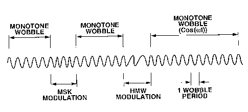
In the present embodiment of the optical disc 1, shown in Fig.3, a block
comprised of a predetermined number of consecutive periods of a sinusoidal
carrier
signal waveform of a predetermined frequency is formed, and a wobble signal
having
an MSK modulated portion and an HMW modulated portion is generated in the
block.
In the MSK modulated portion and in the HMW modulated portion, the MSK
modulated address information and the HMW modulated address information are
inserted, respectively. That is, the MSK modulated address information and the
HMW
modulated address information are inserted in different positions in the
block. One of
the two sinusoidal carrier signals used in the MSK modulation and the carrier
signal
of the HMW modulation correspond to the aforementioned reference carrier
signal.
The MSK modulated portion and the HMW modulated portions are arranged at
different positions in the block, there being arranged a reference carrier
signal of not
less than one period of the reference carrier signal between the MSK
modulation
portion and the HMW modulation portion.
CA 02430904 2003-06-03
WO 03/034414 PCT/JP02/10558
12
Meanwhile, the portion of the block not subjected to data modulation and in
which only the frequency component of the reference carrier signal is
presented is
termed a monotone wobble. The sinusoidal signal used as the reference carrier
signal
is cos(c)t). One period of the reference carrier signal is termed one wobble
period.
The frequency of the reference carrier signal is constant from the inner to
the outer
rims and is determined in relation to the linear velocity of movement of the
laser spot
along the recording track.
The methods for MSK modulation and HMW modulation are further explained
in detail.
1-2 MSK modulation
First, the modulation system of the address information employing the MSK
modulation system is explained.
The MSK modulation is the continuous-phase FSK (frequency shift keying)
modulation with the modulation index of 0.5. In the FSK modulation, the codes
"0"
and "1" of the data for modulation are associated with two carrier signals,
namely a
carrier signal with a frequency fl and a carrier signal with a frequency f2
for
modulation, respectively. That is, the FSK modulation system is such a system
in
which a sinusoidal waveform with the frequency fl is output if the data for
modulation
is "0" and a sinusoidal waveform with the frequency f2 is output if the data
for
modulation is "1". Moreover, in the continuous-phase FSK modulation, the two
carrier signals are phase-continuous or same in phase at the code switching
timing of
CA 02430904 2003-06-03
WO 03/034414 PCT/JP02/10558
13
the data for modulation.
In this FSK modulation, the modulation index in is defined. Specifically, the
modulation index in is defined by
m= Ifl -f2JT
where T is the rate of transmission of the data for modulation (I /time of the
shortest
code length). The continuous FSK modulation for in = 0.5 is termed the MSK
modulation.
In the present optical disc 1, the shortest code length L of the data for
modulation, subjected to the MSK modulation, is equal to two wobble periods,
as
shown in Figs.4A and 4B. Meanwhile, the shortest code length L of the data for
modulation may be any optional length provided that it is an integral number
times the
wobble period and not less than twice the wobble period. On the other hand,
one of
the two frequencies used in MSK modulation is the same as the frequency of the
reference carrier signal, with the other frequency being 1.5 times the
frequency of the
reference carrier signal. That is, one of the signal waveforms used for MSK
modulation is cos(Wt) or -cos(Wt), with the other being cos(1.5Wt) or -
cos(1.5wt).
In inserting the data for modulation in the MSK modulation system into the
wobble signal of the optical disc 1, a data stream of the data for modulation
is
subjected to differential encoding processing in terms of a clock
corresponding to the
wobble period as a unit, as shown in Fig.4C. That is, the stream of the data
for
modulation and delayed data delayed by one period of the reference carrier
signal are
CA 02430904 2003-06-03
WO 03/034414 PCT/JP02/10558
14
subjected to differential encoding processing. The data resulting from the
differential
encoding processing is precode data.
This precode data is MSK modulated to generate an MSK stream. As shown
in Fig.4D, the signal waveformn of this MSK stream is the waveform of the same
frequency as the reference carrier or cos((ot) or its inverted wavefonn -
cos(wt) if the
precode data is "0", while being the waveform of the fi-equency 1.5 times the
frequency of the reference carrier or cos(1.5(ot) or its inverted waveform -
cos(1.5wt)
) if the precode data is "1". Thus, if the data string of the data for
modulation is of a
pattern "010" as shown in Fig.4B, the signal waveform of the MSK stream is
cos((ot),
cos(6)t), cos(1.5wt), -cos(6)t), -cos(1.56)t), cos(wt), every wobble period,
as shown in
Fig.4E.
In the present optical disc 1, the wobble signal is modulated with the address
information by rendering the wobble signal the aforementioned MSK stream. So,
the
conversion of data from Fig.4B to Fig.4D is termed modulation and the
conversion of
data in the opposite direction is termed demodulation.
If the data for modulation is differential-coded by way of performing the
aforementioned MSK modulation, synchronous detection of the data for
modulation
becomes possible. The synchronous detection becomes possible for the following
reason:
With the differential-coded data (precode data), the bit asserts itself
(becomes
"1") at a code change point of the data for modulation. Since the code length
of the
CA 02430904 2003-06-03
WO 03/034414 PCT/JP02/10558
data for modulation is selected to be not less than twice the wobble period,
the
reference carrier signal (cos(wt)) or its inverted signal (-cos(6)t)) is
necessarily
inserted into the latter half of the code length of the data for modulation.
If the bit of
the precode data is "l", the waveform of a frequency 1.5 times that of the
reference
carrier signal is inserted and, at the code switching timing, the data before
switching
is in phase with that after switching. Therefore, the signal waveform inserted
into the
latter half of the code length of the data for modulation is necessarily the
waveform
of the reference carrier signal (cos(6)t)) if the data for modulation is "0",
whereas, if
the data for modulation is "1", the signal waveform is necessarily its
inverted signal
(-cos(6)t)). The synchronous detection output is of a plus value if the data
for
modulation is in phase with the carrier signal, while being of a minus value
if the data
for modulation is inverted in phase. Thus, the data for modulation can be
demodulated
if the MSK modulated signal described above is subjected to synchronous
detection
with the reference carrier signal.
Meanwhile, in the MSK modulation, modulation occurs in an in-phase state at
the code switching positions. Thus, a delay is produced until the synchronous
detection signal is inverted in level. Therefore, if the signal MSK-modulated
as
described above is to be demodulated, an integrating window of the synchronous
detection output is delayed by one-half the wobble period to produce a
correctly
detected output.
Fig.5 shows an MSK demodulating circuit for demodulating the data for
CA 02430904 2003-06-03
WO 03/034414 PCT/JP02/10558
16
modulation from the above-mentioned MSK stream.
An MSK demodulating circuit 10 includes a PLL circuit 11, a timing generator
(TG) 12, a multiplier 13, an integrator 14, a sample-and-hold (SH) circuit 15
and a
slicing circuit 16, as shown in Fig. 5.
The PLL circuit 11 is fed with a wobble signal (MSK modulated stream). The
PLL circuit 11 detects edge components from the input wobble signal to
generate
wobble clocks synchronized with the reference carrier signal (cos(o t)). The
so
generated wobble clocks are sent to the timing generator 12.
The timing generator 12 generates the reference carrier signal (cos(cot))
synchronized with the input wobble signal. The timing generator 12 also
generates a
clear (CLR) signal and a hold (HOLD) signal from the wobble clocks. The clear
(CLR) signal is generated at a timing delayed by one-half wobble period from
the
leading edge of a data clock of the data for modulation the minimum code
length of
which is two wobble periods. The hold signal (HOLD) is a signal generated at a
timing
delayed one-half wobble period from the end edge of the data clock of the data
for
modulation. The reference carrier signal (cos(6)t)), generated by the timing
generator
12, is sent to the multiplier 13. The generated clear signal (CLR) is sent to
the
integrator 14, while the generated hold signal (HOLD) is sent to the sample-
and-hold
circuit 15.
The multiplier 13 multiplies the input wobble signal with the reference
carrier
signal (cos(wt)) to execute synchronous detection. The synchronous detected
output
CA 02430904 2003-06-03
WO 03/034414 PCT/JP02/10558
17
signal is sen to the integrator 14.
The integrator 14 integrates the synchronous detected signal by the multiplier
34. Meanwhile, the integrator 14 clears the integrated value to zero at a
generating
timing of the clear signal (CLR) produced by the timing generator 12.
The sample-and-hold circuit 15 samples the integrated output value of the
integrator 14 at a generating timing of the hold signal (HOLD) produced by the
timing
generator 12 to hold the sampled value until generation of the next hold
signal
(HOLD).
The slicing circuit 16 binary-encodes the value held by the sample-and-hold
circuit 15, with a point of origin (0) as a threshold value, and inverts the
sign of the
encoded value to output the resulting signal.
The output signal of the slicing circuit 16 becomes the data for modulation of
the data for modulation.
Figs.6 and 7 show the wobble signal (MSK stream) generated on MSK
modulation of a data string "0100" as data for modulation and output signal
waveforms
of respective circuits of the MSK demodulating circuit 10 when the wobble
signal is
fed to this MSK demodulating circuit 10. In Figs.6 and 7, the abscissa (n)
denotes the
period numbers of the wobble periods. Fig.6 shows the input wobble signal (MSK
stream) and the synchronous detection output signal of the wobble signal (MSKx
cos((ot)). Fig.7 shows an integrated output value of the synchronous detected
output
signal, a sample-held value of the integrated output value and the data for
modulation
CA 02430904 2003-06-03
WO 03/034414 PCT/JP02/10558
18
output demodulated from the slicing circuit 16. Meanwhile, the data for
modulation
of the data for modulation, output from the slicing circuit 16, is delayed
because of the
processing delay caused in the integrator 14.
If the data for modulation is differential-encoded and subjected to the above-
described MSK-modulation, synchronous detection of the data for modulation
becomes possible, as described above.
In the present optical disc 1, the address information, MSK-modulated as
described above, is formed into the wobble signal. By MSK modulating the
address
information and by having the so modulated address information formed into the
wobble signal, the content of harmonics in the wobble signal is decreased,
thus
enabling accurate address detection. Moreover, since the MSK modulated address
information is inserted in the monotone wobble, the crosstalk given to the
neighboring
track, may be reduced thus improving the S/N ratio. In addition, in the
present optical
disc 1, since the MSK data for modulation may be demodulated on synchronous
detection, the wobble signal can be demodulated correctly and readily.
1-3 HMW modulation
The modulation system for the address information, employing the HMW
modulation system, is hereinafter explained.
The HMW modulation system is such a system in which signals of even
harmonics are added to the sinusoidal carrier signal and in which the polarity
of the
even harmonics signal is varied depending on the sign of the data for
modulation to
CA 02430904 2003-06-03
WO 03/034414 PCT/JP02/10558
19
modulate the digital code.
With the present optical disc 1, the carrier signal of the HMW modulation is
the
signal of the same frequency and phase as those of the reference carrier
signal
(cos(Wt)) which is the carrier signal used in the above-described MSK
modulation.
The even harmonics signals to be added are sin(26)t) and -sin(26)t) as second
harmonics of the reference carrier signal (cos(c)t)), with the amplitudes
thereof being
-12dB with respect to the amplitude of the reference carrier signal. The
minimum
code length of the data for modulation is twice the wobble period (period of
the
reference carrier signal).
If the sign of the data for modulation is "1", sin(2wt) is added to the
carrier
signal, whereas, if the sign of the data for modulation is "0", -sin(2(jt) is
added to the
carrier signal, for modulation.
Fig.8 shows the signal waveform in case the wobble signal is modulated by the
above-described system. Fig.8A shows the signal waveform of the reference
carrier
signal (cos((ot)), while Fig. 8B shows the signal waveformn obtained on adding
sin(26)t)
to the reference carrier signal (cos(Wt)), that is the signal wavefonn in case
the data for
modulation is "1". Fig. 8C shows the signal waveform obtained on adding -
sin(26)t)
to the reference carrier signal (cos(wt)), that is the signal wavefonn in case
the data for
modulation is "0".
In the present optical disc 1, the harmonics signal added to the carrier
signal is
second harmonics. However, any optional even hannonics may be added in place
of
CA 02430904 2003-06-03
WO 03/034414 PCT/JP02/10558
the second harmonics. Moreover, although only the second hannonics are added
in
the present optical disc 1, plural harmonics signals, such as second and
fourth
harmonics, may be added simultaneously.
If the positive or negative even harmonics are added to the reference carrier
signal, as described above, the data for modulation can be demodulated, by
synchronous detection with the harmonics signals and by integration of the
synchronous-detected output for the code length time of the data for
modulation.
Fig.9 shows an HMW modulation circuit for demodulating the data for
modulation from the wobble signal HMW modulated as described above.
An HMW demodulating circuit 20 includes a PLL circuit 21, a timing generator
(TG) 22, a multiplier 23, an integrator 24, a sample-and-hold circuit (SH) 25
and a
slicing circuit 26, as shown in Fig.9.
The PLL circuit 21 is fed with a wobble signal (HMW modulated stream). The
PLL circuit 21 detects edge components from the input wobble signal to
generate
wobble clocks synchronized with the reference carrier signal (cos(Wt)). The so
generated wobble clocks are sent to the timing generator 22.
The timing generator 22 generates second hannonics signal (sin(26)t))
synchronized with the input wobble signal. The timing generator 22 also
generates
a clear signal (CLR) and a hold signal (HOLD). The clear signal (CLR) is a
signal
generated at a timing of a rising edge of a data clock of the data for
modulation having
two wobble periods as its minimum code length. The hold signal (HOLD) is a
signal
CA 02430904 2003-06-03
WO 03/034414 PCT/JP02/10558
21
generated at the falling edge of the data clock of the data for modulation.
The second
harmonics (sin(2 (ot)), produced by the timing generator 22, is sent to the
multiplier 23.
The clear signal (CLR) generated is routed to the integrator 24, while the
hold signal
(HOLD) generated is sent to the sample-and-hold circuit 25.
The multiplier 23 multiplies the input wobble signal with the second harmonics
(sin(2Wt)) to perform synchronous detection. The synchronous-detected output
signal
is sent to the integrator 24.
The integrator 24 integrates the signal synchronous-detected by the multiplier
23. Meanwhile, the integrator 24 clears the integrated value to zero at a
generating
timing of the clear signal (CLR) by the timing generator 22.
The sample-and-hold circuit 25 samples the integrated output value of the
integrator 24 at a generating timing of the hold signal (HOLD) produced by the
timing
generator 22 to hold the sampled value until generation of the next hold
signal
(HOLD).
The slicing circuit 26 binary-encodes the value held by the sample-and-hold
circuit 25, with a point of origin (0) as a threshold value, and outputs the
resulting
encoded signal.
The output signal of the slicing circuit 26 becomes the data for modulation of
the data for modulation.
Figs. 10 to 12 show a signal wavefonn used in HMW modulating a data string
"1010" as data for modulation, a wobble signal generated on HMW modulation and
CA 02430904 2003-06-03
WO 03/034414 PCT/JP02/10558
22
output signal waveforms from respective circuits in case the wobble signal is
fed to the
HMW demodulating circuit 20. In Figs. 10 to 12, the abscissa (n) denotes the
period
numbers of the wobble periods. Fig. 10 shows the reference carrier signal
(cos(6)t)),
a data string "1010" as data for modulation and second harmonics signal
waveforms
( sin(2wt), -12dB) generated in meeting with the data for modulation. Fig. 11
shows
the generated wobble signal (HMW stream). Fig. 12A shows the synchronous-
detected
output signal of the wobble signal (HMW x sin(2wt)), whilst Fig. 12B shows an
integrated output value of the synchronous-detected output signal, a sample-
held value
of the integrated output and data for modulation output from the slicing
circuit 26.
Meanwhile, the data for modulation, output from the slicing circuit 26, is
delayed
because of the first order delay caused in the integrator 14.
If the data for modulation is differential-encoded and MSK-modulated as
described above, synchronous detection of the data for modulation becomes
possible.
In the present optical disc 1, the address information, HMW-modulated as
described above, is formed into the wobble signal. By HMW modulating the
address
information, and by having the so modulated address information formed into
the
wobble signal, it is possible to limit frequency components and the reduce
high
harmonics components. The result is that the S/N ratio of the demodulated
output of
the wobble signal can be improved and addresses can be detected correctly.
Moreover, the modulating circuit can be constructed by a carrier signal
generating
circuit, a circuit for generating its hannonics components and a circuit for
summing
CA 02430904 2003-06-03
WO 03/034414 PCT/JP02/10558
23
the outputs of these circuits, and thus may be simpler in structure.
Additionally, the
high frequency components of the wobble signal can be reduced to facilitate
cutting
in molding an optical disc.
Since the HMW modulated address information is inserted into the monotone
wobble, it is possible to reduce the crosstalk applied to the neighboring
tracks to
improve the S/N ratio. Moreover, in the present optical disc, since the HMW
data for
modulation can be demodulated on synchronous detection, the wobble signal can
be
demodulated accurately and extremely readily.
1-4 Suin
In the present embodiment of the optical disc, described above, the MSK
modulation system and the HMW modulation system are used as the modulation
systems for modulating the wobble signal with the address information. In the
present
optical disc 1, one of the frequencies used in the MSK modulation system and
the
carrier frequency used in the HMW modulation are the sinusoidal signal of the
same
frequency (cos(6)t)). Moreover, the monotone wobble including only the carrier
signal
(cos(wt)), and which is free of data for modulation, is provided between
respective
modulated signals in the wobble signal.
In the above-described optical disc 1, there is no interference produced
between
the signal of the frequency used in MSK modulation and the harmonics used for
HMW
modulation, so that, in detection, the respective modulation components are
not
affected by counterpart modulation components. Thus, the respective address
CA 02430904 2003-06-03
WO 03/034414 PCT/JP02/10558
24
information, recorded by the two modulation systems, can be detected reliably.
The
result is the improved accuracy in controlling e.g., the track positions in
recording
and/or reproducing the optical disc.
If the address information recorded by MSK modulation is of the same data
contents as the address information recorded by HMW modulation, the address
information can be detected more reliably.
Moreover, in the present optical disc 1, since one of the frequencies used in
the
MSK modulation system and the carrier frequency used in the HMW modulation are
the same frequency of the sinusoidal signals (cos(wt)), and the MSK modulation
and
the HMW modulation are applied to different portions in the wobble signal, it
is
sufficient in modulation if harmonics signals for HMW modulation are added to
a
wobble position of the MSK modulated wobble signal which is intended for HMW
modulation, thus assuring highly facilitated MSK and HMW modulations.
Moreover,
since the MSK modulation and the HMW modulation are applied to different
portions
in the wobble signal and at least one period of the monotone wobble is
provided
between the two modulations, it is possible to realize more accurate disc
manufacture
and more reliable address demodulation.
2. Instance of Application to DVR
An instance of application of the aforementioned address format to a high
density optical disc termed DVR (data and video recording) is hereinafter
explained.
2-1 Physical Characteristics of DVR Disc
CA 02430904 2003-06-03
WO 03/034414 PCT/JP02/10558
First, typical physical parameters of a DVR disc, to which the present address
format is applied, are explained. Meanwhile, these physical parameters are
merely
illustrative such that the wobble format now explained may also be applied to
an
optical disc of any other suitable physical characteristics.
The DVR disc of the present embodiment is an optical disc for recording data
in accordance with the phase change system. The disc size is 120 lain in
diameter,
with the disc thickness being 1.2 mm.
The area on the disc is composed of a lead-in area, a program area and a lead-
out area, looking from the inner peripheral side. The information area, made
up of
these areas, is formed at a diametrical position ranging from 44 inm to 117
min.
For recording and/or reproduction, the so-called blue laser light of 405 nm is
used. The NA of a lens is 0.85, with the track pitch being 0.30 m, a channel
bit
length being 0.086 m and a data bit length being 0.13 inn. The average
transfer rate
of the user data is 35 Mbits/sec.
The user data capacity is 22.46 Gbytes.
Data recording is by a groove recording system. That is, a track is formed at
the
outset on the disc by a groove, on which recording is to be made. This groove
is
wobbled to record the address information of the present disc.
2-2 Format of Data for Recording and/or Reproduction
The error correction block (ECC block) of phase change data of the present
embodiment of the DVR disc is 64 kbytes (304 bytes x248 bytes), as shown in
Fig. 13.
CA 02430904 2003-06-03
WO 03/034414 PCT/JP02/10558
26
This ECC block is made up of 304 rows by 2l6columns of data, and 304 rows by
32
columns of parity, with one symbol being one byte. The parity is generated by
long
distance Reed-Solomon coding of LDC (248, 216, 33) of 304 rows by 216 columns
of
data with respect to the column direction.
Meanwhile, in the present embodiment of the DVR disc, the recording and/or
reproducing unit of the phase change data may be 2k bytes. In this case,
recording
and/or reproduction is performed with the aforementioned 64 kbytes of the
error
correction block, and data rewriting is performed on desired 2k bytes of the
error
correction block.
Turning to the recording and/or reproducing unit of the present embodiment of
the DVR disc, the ECC block is an ECC block cluster of 156 symbols by 496
frames,
as shown in Fig. 14, and a one-frame link area for e.g., PLL is appended to
each of the
leading and trailing sides of the ECC block cluster to form a sum total of 498
frames
of the recording and/or reproducing cluster. This recording and/or reproducing
cluster
is termed an RUB (recording unit block).
Each frame of each ECC block cluster is made up of data symbols, split in
terms
of 38 bytes as a unit, and Sync codes or BIS (burst indicator subcode)
inserted
between the respective data symbols. Specifically, each frame is made up of a
Sync
code, a data symbol (38 bytes), BIS, a data symbol (38 bytes), BIS, a data
symbol (38
bytes), BIS, a data symbol (38 bytes), in this order, looking from the leading
side. The
BIS and Sync codes may be used for discriminating burst errors in data
reproduction.
CA 02430904 2003-06-03
WO 03/034414 PCT/JP02/10558
27
That is, if the continuous Sync and BIS represent symbol errors, the 38 bytes
of the
data symbol, sandwiched by the Sync and BIS, corrupted with errors, is also
deemed
to be corrupted with burst errors, and pointer erasure correction is performed
accordingly.
2-3 Address Format
2-3-1 Relationship between Data for Recording and/or Reproduction and
Addresses
In the present address format, the sole RUB (498 frames) is managed by three
address units (ADIP_l, ADIP_2 and ADIP_3), recorded as wobble, as shown in
Fig. 15. That is, a sole RUB is recorded for these three address units.
In the present address format, the sole address unit is formed by an 8-bit
sync
part and 75 bits of a data part, totaling at 83 bits. In the present address
format, the
reference carrier signal of the wobble signal recorded on the pre-groove is
the cosine
signal (cos(6)t)), with one bit of the wobble signal being formed by 56
periods of the
reference carrier signal, as shown in Fig. 16. The `bit' herein means one bit
of the
information represented by the wobble signal. Thus, the length of one period
of the
reference carrier signal (one wobble period) is 69 times one channel length of
the
phase change. The 56 periods of the reference carrier signal forming one bit
is
referred to below as a bit block.
2-3-2 Sync Part
Fig. 17 shows a bit configuration of the sync part in the address unit. The
sync
part is a portion for identifying the leading end of an address unit and is
made up of
CA 02430904 2003-06-03
WO 03/034414 PCT/JP02/10558
28
four, namely first to fourth sync blocks (sync block "1," sync block "2," sync
block
"3" and sync block "4"). Each sync block is formed by a monotone bit and a
sync bit,
totaling to two bit blocks.
Turning to the signal waveform of the monotone bit, shown in Fig. 1 SA, the
first
to third wobbles of the bit block made up of 56 wobbles represent a bit
synchronization mark BM, with the fourth to 56th wobbles as from the
synchronization mark BM being monotone wobbles (signal waveform of the
reference
carrier signal (cos((ot)).
The bit synchronization mark BM is a signal wavefonn obtained on MSK
modulating the data for modulation of a predetermined code pattern designed
for
discriminating the leading end of a bit block. That is, this bit
synchronization mark
BM is a signal waveform generated on differential encoding of data for
modulation of
a predetermined code pattern and assigning the frequency depending on the sign
of the
differential encoded data. Meanwhile, the minimum code length L of the data
for
modulation is two wobble periods. In the present embodiment, the signal
waveform
obtained on MSK modulating the data for modulation with one bit (two wobble
periods) of "1" is recorded as the bit synchronization mark BM. That is, this
bit
synchronization mark BM is a signal waveform continuous, in terms of a wobble
period as a unit, as "cos(1.5Wt), -cos(cot) and -cos(1.56)t)".
So, the monotone bit can be generated by generating data for modulation such
as "10000===00", with the code length being two wobble periods, and by MSK
CA 02430904 2003-06-03
WO 03/034414 PCT/JP02/10558
29
modulating this data for modulation, as shown in Fig. 18B.
It should be noted that the bit synchronization mark BM is inserted not only
at
the leading end of the monotone bit of the sync part but also at the leading
end of each
of all bit blocks as now explained. Thus, during recording and/or
reproduction, this
bit synchronization mark BM may be detected and synchronized for
synchronization
of the bit blocks in the wobble signal, that is synchronization of the 56
wobble periods.
Moreover, the bit synchronization mark BM may be used as a reference for
specifying
the inserting positions in the bit block of various signals for modulation as
hereinafter
explained.
In the signal waveform of the sync bit of the first sync block (sync "0" bit),
the
first to third wobbles of the 56 wobbles making up a bit block represent the
bit
synchronization mark BM, and the 17th to 19th wobbles and the 27th to 29th
wobbles
thereof represent MSK modulation marks MM, with the waveform of the remaining
wobbles being all monotone wobbles, as shown in Fig. 19A.
In the signal waveform of the sync bit of the second sync block (sync " 1"
bit),
the first to third wobbles of the 56 wobbles making up a bit block represent
the bit
synchronization mark BM, and the 19th to 21st wobbles and the 29th to 31st
wobbles
thereof represent MSK modulation marks MM, with the waveform of the remaining
wobbles being all monotone wobbles, as shown in Fig.20A.
In the signal waveform of the sync bit of the third sync block (sync "2" bit),
the first to third wobbles of the 56 wobbles making up a bit block represent
the bit
CA 02430904 2003-06-03
WO 03/034414 PCT/JP02/10558
synchronization mark BM, and the 21st to 23rd wobbles and the 31st to 33rd
wobbles
thereof represent MSK modulation marks MM, with the waveform of the remaining
wobbles being all monotone wobbles, as shown in Fig.21A.
In the signal wavefonn of the sync bit of the fourth sync block (sync "3"
bit),
the first to third wobbles of the 56 wobbles making up a bit block represent
the bit
synchronization mark BM, and the 23rd to 25th wobbles and the 33rd to 35th
wobbles
thereof represent MSK modulation marks MM, with the waveform of the remaining
wobbles being all monotone wobbles, as shown in Fig.22A.
Similarly to the bit synchronization mark BM, the MSK modulation mark MM
is a signal waveform generated on MSK modulating the data for modulation of a
predetermined code pattern. That is, this MSK modulation mark MM is a signal
waveform generated on differential encoding of data for modulation of a
predetermined code pattern and on assigning the frequency depending on the
sign of
the differential-encoded data. Meanwhile, the minimum code length L of the
data for
modulation corresponds to two wobble periods. In the present instance, the
signal
waveform, obtained on MSK modulating the data for modulation, having one bit,
corresponding to two wobble periods, set to "1", is recorded as the MSK
modulation
mark MM. That is, this MSK modulation mark MM is a continuous waveform,
composed of "cos(1.5wt), -cos(wt) and -cos(1.5o t)", in terms of one wobble
period
as a unit.
That is, the sync bit of the first sync block (sync "0" bit) can be generated
on
CA 02430904 2003-06-03
WO 03/034414 PCT/JP02/10558
31
generating a data stream shown in Fig. 19B (with the code length being two
wobble
periods) and on MSK modulating the so generated data stream. Similarly, the
sync bit
of the second sync block (sync "1" bit), sync bit of the third sync block
(sync "2" bit)
and the sync bit of the fourth sync block (sync "2" bit) can be generated on
generating
the data stream shown in Fig.20B and on MSK modulation thereof, on generating
the
data stream shown in Fig.21B and on MSK modulation thereof and on generating
the
data stream shown in Fig.22B and on MSK modulation thereof, respectively.
Meanwhile, the sync bit insertion pattern to a bit block of two MSK modulation
marks MM is unique with respect to the insertion pattern of the MSK modulation
marks MM in the remaining bit blocks. Thus, during recording and/or
reproduction,
the address unit can be synchronized by MSK demodulating the wobble signals,
verifying the insertion pattern of the MSK modulation marks MM in the bit
block and
by discriminating at least one of the four sync bits, thereby achieving
demodulation
and decoding of the data part as now explained.
2-3-3 Data Part
Fig.23 shows a bit configuration of the data part in the address unit. The
data
part holds real data of the address information and is made up of 15, namely
the first
to 15th ADIP blocks (ADIP block " 1" to ADIP block "15"). Each ADIP block is
made
up of one monotone bit and four ADIP bits.
The signal waveform of the monotone bit is similar to that shown in Fig. 18.
The ADIP bit denotes one bit of real data. The signal waveform is changed with
CA 02430904 2011-08-18
32
code contents of the real data bit.
If the sign content, denoted by the ADIP bit, is "1", the first to third
wobbles,
the 13th to 15th wobbles and the 19th to 55th wobbles of the bit block, made
up of 56
wobbles, become the bit synchronization mark BM, MSK modulation mark MM and
the modulation part of HMW "1" composed of the reference carrier signal
(cos(c)t)) and
sin(2o)t) added thereto, respectively, with the waveform of the remaining
wobbles
being all monotone wobbles. That is, the ADIP bit, the sign content of which
is "I",
can be generated by generating data for modulation such as "100000100==.00"
with the
code length being two wobble periods, MSK modulating the so generated data for
modulation, as shown in Fig. 24B, and by adding sin(2(ot), with an amplitude
equal to
-12dB, to the 19th to 55th wobbles of the HMW modulated signal waveform, as
shown in Fig. 24C.
If the sign content denoting the ADIP bit is "0", the first to third wobbles,
the
15th to 17th wobbles and the 19th to 55th wobbles of the bit block, made up of
56
wobbles, become bit synchronization mark BM, MSK modulation mark MM and the
modulation part of HMW "0" comprised of the reference carrier signal
(cos((ot)) and
-sin(2(Jt) added thereto, respectively, with the waveform of the remaining
wobbles
being all monotone wobbles. That is, the ADIP bit, the sign content of which
is "0",
can be generated by generating data for modulation such as "100000010==.00"
with the
code length being two wobble periods, and MSK modulating the so generated data
for
modulation, as shown in Fig. 25B, and by adding -sin(2cot), with an amplitude
equal
CA 02430904 2011-08-18
33
to -12dB, to the 19th to 55th wobbles of the HMW modulated signal waveform, as
shown in Fig. 25C.
The ADIP bit has its bit contents distinguished depending on the inserting
positions of the MSK modulation mark MM. That is, if the MSK modulation mark
MM is inserted at the 13th to 15th wobbles, it indicates a bit "1", whereas,
if the MSK
modulation mark MM is inserted at the 15th to 17th wobbles, it indicates a bit
"0".
Moreover, the ADIP bit denotes, by the HMW modulation, the same bit content as
the
bit content represented by the inserting position of the MSK modulation mark
MM.
Therefore, the ADIP bit denotes the same bit contents for the two different
modulation
systems, thus assuring reliable data decoding.
Fig. 26 shows the format of the address unit showing the above-described sync
and data parts synthesized together.
In the address format of the present optical disc 1, the bit synchronization
mark
BM, the MSK modulation mark MM and the HMW modulating part are arranged
discretely in one address unit, as shown in Fig. 26. Between the modulated
signal
portions is arranged at least one wobble period of the monotone wobble. As a
result,
there no risk of interference between respective modulation signals, thus
assuring
reliable demodulation of respective signals.
2-3-4 Contents of Address Information
Fig. 27 shows the contents of the address information represented by the ADIP
bit in the data part. In one address unit, there are contained 60 (4x15) ADIP
bits, such
CA 02430904 2003-06-03
WO 03/034414 PCT/JP02/10558
34
that there are shown information contents of 60 bits for a data string. This
60-bit
address information is made up of a 3-bit layer information (Layer) indicating
the layer
numbers in case of multi-layered recording, a 19-bit RUB information (RUB)
indicating the RUB address, 2-bit address number information (address
number/RUB)
indicating the numbers of the address units in the RUB, the 12-bit auxiliary
information (Aux data) stating e.g., the recording conditions, such as
recording
patterns, and the 24-bit parity information (parity), as shown in Fig.27.
The 24-bit parity is the so-called nibble base Reed-Solomon code, having 4
bits
as one symbol (RS(15, 9, 7)). Specifically, error correction coding is
performed with
the code length of 15 nibbles, data of 9 nibbles and parity of 6 nibbles, as
shown in
Fig.28.
2-4 Address Demodulating circuit
An address demodulating circuit for demodulating the address information from
the DVR disc of the aforementioned address format is hereinafter explained.
Fig.29 shows a block structure of an address demodulating circuit.
The address demodulating circuit 30 includes a PLL circuit 31, a timing
generator for MSK 32, a multiplier for MSK 33, an integrator for MSK 34, a
sample-
and-hold circuit for MSK 35, a slicing circuit for MSK 36, a sync decoder 37,
an MSK
address decoder 38, a timing generator for HMW 42, a multiplier for HMW 43, an
integrator for HMW 44, a sample-and-hold circuit for HMW 45, a slicing circuit
for
HMW 46 and an address decoder for HMW 47, as shown in Fig.29.
CA 02430904 2003-06-03
WO 03/034414 PCT/JP02/10558
The PLL circuit 31 is fed with the wobble signal reproduced from the DVR
disc. The PLL circuit 31 detects edge components from the input wobble signal
to
generate wobble clocks synchronized with the reference carrier signal
(cos(6)t)). The
so generated wobble clocks are sent to the timing generator for MSK 32 and to
the
timing generator for HMW 42.
The timing generator for MSK 32 generates the reference carrier signal
(cos(wt)) synchronized with the input wobble signal. The timing generator for
MSK
32 also generates a clear signal (CLR) and a hold signal (HOLD) from the
wobble
clocks. The clear signal (CLR) is such a signal generated at a timing delayed
one-half
wobble period as from the leading edge of the data clock of the data for
modulation
having the minimum code length equal to two wobble periods. The hold signal
(HOLD) is such a signal generated at a timing delayed one-half wobble period
as from
the trailing edge of the data clock of the data for modulation. The reference
carrier
signal (cos(6)t)), generated by the timing generator for MSK 32, is sent to
the
multiplier for MSK 33. The generated clear signal (CLR) is sent to the
integrator for
MSK 34. The generated hold signal (HOLD) is sent to the sample-and-hold
circuit for
MSK 35.
The multiplier for MSK 33 multiplies the input wobble signal with the
reference
carrier signal (cos(o)t)) by way of performing synchronous detection
processing. The
synchronous-detected output signal is sent to the integrator for MSK 34.
The integrator for MSK 34 integrates the signal synchronous-detected by the
CA 02430904 2003-06-03
WO 03/034414 PCT/JP02/10558
36
multiplier for MSK 33. Meanwhile, the integrator for MSK 34 clears the
integrated
value to "0" at the generation timing of the clear signal (CLR) by the timing
generator
for HMW 42.
The sample-and-hold circuit for MSK 35 samples an integrated output value
of the integrator for MSK 34, at a timing of generation of the hold signal
(HOLD) by
the timing generator for MSK 32, to hold the sampled value until occurrence of
the
next hold signal (HOLD).
The slicing circuit for MSK 36 binary-encodes the value held by the sample-
and-hold circuit for MSK 35, with the point of origin (0) as a threshold
value, and
inverts the sign of the binary-coded value to output the resulting signal.
The output signal of the slicing circuit for MSK 36 becomes an MSK data for
modulation stream.
The sync decoder 37 detects a sync bit in the sync part from the bit pattern
of
the data for modulation output from the slicing circuit for MSK 36. The sync
decoder
37 synchronizes the address unit from the detected sync bit. Based on the
synchronization timing of the address unit, the sync decoder 37 generates an
MSK
detection window, indicating the wobble position of the MSK data for
modulation in
the ADIP bit of the data part, and an HMW detection window indicating the
wobble
position of HMW data for modulation in the ADIP bit of the data part. The
synchronization position timing of the address unit, detected from the sync
bit, the
timing of the MSK detection window and the timing of the HMW detection window,
CA 02430904 2003-06-03
WO 03/034414 PCT/JP02/10558
37
are shown in Figs.30A, 30B and 30C, respectively.
The sync decoder 37 sends the MSK detection window and the HMW detection
window to the MSK address decoder 38 and to the timing generator for HMW 42,
respectively.
The MSK address decoder 38, fed with a demodulated stream output from the
slicing circuit for MSK 36, detects the inserting position of the MSK
modulation mark
MM in the ADIP bit of the data stream demodulated based on the MSK detection
window to check the contents of the sign represented by the ADIP bit. That is,
if the
insertion pattern of the MSK modulation mark of the ADIP bit is a pattern
shown in
Fig.24 or a shown in Fig.25, the contents of the sign are verified to be "1"
or "0",
respectively. The bit string obtained from the results of check is output as
the MSK
address information.
The timing generator for HMW 42 generates the second harmonics (sin(26)t)),
synchronized with the input wobble signal. The timing generator for BMW 42
generates a clear signal (CLR) and a hold signal (HOLD) from the HMW detection
window. The clear signal (CLR) is a signal generated at a timing of the
leading edge
of the HMW detection window. The hold signal (HOLD) is a signal generated at a
timing of the end edge of the HMW detection window. The second harmonics
(sin(2wt)) generated by the timing generator for HMW 42 is sent to the
multiplier for
HMW 43. The clear signal (CLR) generated is sent to the integrator for HMW 44.
The hold signal (HOLD) generated is sent to the sample-and-hold circuit for
HMW 45.
CA 02430904 2003-06-03
WO 03/034414 PCT/JP02/10558
38
The multiplier for HMW 43 multiplies the input wobble signal with the second
harmonics (sin(26)t)) by way of performing synchronous detection processing.
The
synchronous-detected output signal is sent to the integrator for HMW 44.
The integrator for HMW 44 performs integrating processing on the signal
synchronous-detected by the multiplier for HMW 43. This integrator for HMW 44
clears the integrated value to "0" at a timing of generation of the clear
signal (CLR)
by the timing generator for HMW 42, and holds the sampled value until
occurrence of
the next hold signal (HOLD).
The sample-and-hold circuit for HMW 45 samples an integrated output value
of the integrator for HMW 44 at a timing of generation of the hold signal
(HOLD) by
the timing generator for HMW 42, such as to hold the sampled value until
occurrence
of the next hold signal (HOLD). That is, the HMW data for modulation has 37
wobbles in one bit block, so that, if the clear (HOLD) signal is generated at
n = 0, n
being the number of wobbles, as shown in Fig.30D, the sample-and-hold circuit
for
HMW 45 samples the integrated values at n = 36, as shown in Fig.30E.
The slicing circuit for HMW 46 binary-encodes the value held by the sample-
and-hold circuit for HMW 45, with the point of origin (0) as threshold value,
to output
the resulting binary-coded value.
An output signal of the slicing circuit for HMW 46 becomes the data for
modulation stream.
The address decoder for HMW 47 verifies the contents of the code represented
CA 02430904 2003-06-03
WO 03/034414 PCT/JP02/10558
39
by each ADIP bit from the data for modulation stream. The bit string obtained
from
the verified result is output as the HMW address information.
Fig. 31 shows the signal waveform when the ADIP bit with the code contents "
1"
is HMW demodulated by the HMW address decoder 47. The abscissa (n) of Fig.31
shows the period numbers of the wobble periods. Fig.31A shows the reference
carrier
signal (cos((ot)), data for modulation having the code contents "1" and second
harmonics signal waveforms (sin(26t), -12dB), generated in meeting with the
data for
modulation. Fig. 3lB shows generated wobble signal. Fig.31C shows a
synchronous-
detected output signal (HMWxsin(2wt)) of the wobble signal, an integrated
output
value of the synchronous-detected output signal, a sample-held value of the
integrated
output and the data for modulation output by the slicing circuit for HMW 46.
Fig.32 shows the signal waveform when the ADIP bit with the code contents "0"
is HMW demodulated by the HMW address decoder 47. The abscissa (n) of Fig.32
shows the period numbers of the wobble periods. Fig.32A shows the reference
carrier
signal (cos(Wt)), data for modulation having the code contents "1" and second
harmonics signal waveforms (-sin(2wt), -12dB) generated in meeting with the
data for
modulation. Fig.32B shows generated wobble signal. Fig.32C shows a synchronous-
detected output signal (HMWxsin(2wt)) of the wobble signal, an integrated
output
value of the synchronous-detected output signal, a sample-held value of the
integrated
output and the data for modulation output by the slicing circuit for HMW 46.
As described above, the address decoder 47 detects the synchronization
CA 02430904 2003-06-03
WO 03/034414 PCT/JP02/10558
information of the address unit recorded by the MSK modulation and effects MSK
demodulation and HMW demodulation based on the detection timing.
3. Illustrative Structure of Optical Disc Drive
An illustrative structure of an optical disc drive, configured for recording
and/or
reproducing data for a phase change optical disc, to which the above-described
address
format is applied, is now explained.
Fig.33 shows a block diagram of the optical disc drive.
The optical disc 1, loaded on a turntable, is run in rotation by a spindle
motor
61 at a constant linear velocity (CLV) at the time of recording and/or
reproduction.
An optical head 62 includes a laser diode, as a laser light source, a
photodetector for detecting the reflected light, an objective lens for
converging the
laser light on the disc, and a bi-axial unit for holding the objective lens
for movement
in the tracking and focussing directions.
A matrix circuit 63 generates playback signals, focussing error signals,
tracking
error signals and wobble signals (push-pull signals) from a signal detected by
the
photodetector of the optical head 62.
A laser driver 64 excites a laser diode in the optical head 62 to emit light.
A servo circuit 65 effects focussing servo control, tracking servo control and
sled servo control, based on the focussing error signals, tracking error
signals and the
sled error signals, as detected by the matrix circuit 63.
A spindle circuit 66 runs the spindle motor 61.
CA 02430904 2003-06-03
WO 03/034414 PCT/JP02/10558
41
Aread-write (RW) circuit 67 performs recording compensation on the recording
data during recording, while generating clocks from the replay signals during
reproduction to binary-encode the replay signals based on the data clocks to
generate
replay data.
A modulation/demodulation circuit 68 performs modulation/demodulation
processing, such as run length limited modulation/demodulation, on data for
recording
and/or reproduction.
An ECC encoder/decoder 69 performs ECC encoding or ECC decoding on the
data for recording and/or reproduction.
A clock generator 60 generates clock timing signals from the wobble signal to
send the so generated clock timing signals to the read-write circuit 67, a
wobble
demodulating circuit 51 and to an address decoder 52.
The demodulating circuit 51 demodulates data modulated into the wobble
signal. The address decoder 52 decodes the address information of the optical
disc 1
from the data for modulation of the demodulating circuit 51. The demodulating
circuit 51 and the address decoder 52 may be configured as shown for example
in
Fig.29.
A system controller 53 controls the various components making up the present
optical disc drive 50.
In the above-described optical disc drive 50, recording and/or reproducing
data
and a control command are exchanged e.g., with an AV system 55.
CA 02430904 2003-06-03
WO 03/034414 PCT/JP02/10558
42
To the above-described optical disc drive 50, a recording command and, for
example, recording data, such as a picture bit stream, such as MPEG2 picture
bit
stream, are sent from the AV system 55. The recording data, sent from the AV
system
55, are ECC-blocked by an ECC encoder/decoder 69 and subsequently subjected to
data modulation for recording by the modulation/demodulation circuit 6 8. The
system
controller 53 acquires the current address information from the address
decoder 52
and, based on this address information, shifts the recording position for the
optical disc
1 to a desired address. The read/write circuit 52 performs recording
compensation on
the recording data and actuates the laser driver 44 at a clock timing
generated by the
clock generator 60 to record data on the optical disc 1.
The optical disc drive 50 is fed during reproduction with a replay command
from the AV system 55. The system controller 53 acquires the current address
information from the address decoder 52 and, based on the so acquired address
information, shifts the replay position for the optical disc 1 to a desired
address. The
signal reproduced from the address are binary-coded by the read/write circuit
67 and
demodulated by the modulation/demodulation circuit 68. An ECC encoder/decoder
69 sends the MPEG2 picture bit stream, obtained on error correction on the
data for
modulation, to the AV system 55.
4. Manufacturing Method for optical Disc
The manufacturing method for the optical disc, to which is applied the above-
described address format, is now explained.
CA 02430904 2003-06-03
WO 03/034414 PCT/JP02/10558
43
The manufacturing process for an optical disc is roughly classified into a so-
called master disc process (mastering process) and a disc forming process
(replication
process). The mastering process is a process up to the completion of a metal
master
disc (stamper) used in the disc forming process, and the disc forming process
is a
process for mass-producing optical discs, by way of duplication of the
stamper, from
the stamper.
In the mastering process, photoresist is coated on a polished glass substrate
to
form a photosensitive film, which is then subjected to cutting for forming
pits or
grooves by light exposure. During the cutting, pit cutting of forming pits or
grooves
in areas corresponding to embossed areas on the radially innermost side of the
disc and
wobble cutting of forming the wobbling grooves in an area corresponding to the
groove-forming area are performed. On completion of the cutting, predetermined
processing, such as development, is performed, after which the information is
transferred, such as by electrocasting, onto the metal surface, to form a
stamper
necessary for duplicating the discs.
Fig.34 shows a cutting device for performing wobble cutting on a master
optical
disc.
A cutting device 70 is made up of an optical unit 82 for irradiating a light
beam
on the substrate 81 coated with the photoresist for cutting, a rotational
driving unit 83
for rotational driving the substrate 81, and a signal processor 84 for
converting input
data into recording signals and for controlling the optical unit 82 and the
rotational
CA 02430904 2003-06-03
WO 03/034414 PCT/JP02/10558
44
driving unit 83.
The optical unit 82 includes a laser light source 71, such as He-Cd laser, and
an
optical modulator 72. The optical unit 82 is responsive to a wobble signal
stream
generated by the signal processor 84 to cut a pre-groove as it causes
meandering of
the laser beam emitted by the laser light source 71.
The rotational driving unit 83 runs the substrate 71 in rotation, so that the
pre-
groove will be formed spirally from the inner rim side, while causing the
substrate 71
to be moved radially in controlled manner.
The signal processor 84 includes, for example, an address generator 73, an
MSK modulator 74, an HMW modulator 75, an adder 76 and a reference clock
generator 77.
The address generator 73 generates the address information for MSK
modulating the pre-groove of the optical disc and the address information for
HMW
modulating the pre-grooves of the optical disc to send the address information
so
produced to an MSK modulator 74 and to an HMW modulator 75.
Based on reference clocks, generated by a reference clock generator 77, the
MSK modulator 74 generates two frequencies, namely cos(c)t) and cos(1.56)t).
The
MSK modulator 74 also generates, from the address information, a data stream
at a
predetermined timing position of which is formed the data for modulation
synchronized with the reference clock. The MSK modulator 74 MSK modulates the
data stream with the two frequencies of cos(Wt) and cos(1.5 Wt) to generate
MSK
CA 02430904 2003-06-03
WO 03/034414 PCT/JP02/10558
modulated signals. In the portion of the data stream in which the address
information
is not subjected to MSK modulation, the MSK modulator 74 generates a signal
with
a waveform of cos(Wt) (monotone wobble).
Based on the reference clocks, generated by the reference clock generator 77,
the HMW modulator 75 generates second harmonics ( sin(2Wt)), synchronized with
cos(c)t) generated by the MSK modulator 74. The HMW modulator 75 outputs the
second harmonics at a timing of recording the address information by HMW
modulation. This timing corresponds to the monotone wobble free of the MSK
modulation. At this time, the HMW modulator 75 outputs +sin(2wt) and -
sin(26)t) in
a switching fashion depending on the digital sign of the input address
information.
The adder 76 adds second harmonics signals, output from the HMW modulator
75, to the MSK modulated signals output from the MSK modulator 74.
The output signal of the adder 76 is sent as the wobble signal stream to the
optical unit 82.
Thus, the cutting device 70 is able to record the wobble, modulated with the
address information, on the optical disc, using two modulating systems, namely
the
MSK modulation system and the HMW modulating system.
Moreover, in the present cutting device 70, one of the frequencies used in the
MSK modulating system and the carrier frequency used in the HMW modulation
represent the sinusoidal wave signal of the same frequency (cos(c)t)) as that
used in
the HMW modulation. In the wobble signal, there is provided a monotone wobble,
CA 02430904 2003-06-03
WO 03/034414 PCT/JP02/10558
46
free of modulating data and containing only the carrier signal (cos(cot)),
between the
wobble signals.
In addition, in the present cutting device 70, one of the frequencies used in
the
MSK modulation system and the carrier frequency used in the HMW modulation
represent the sinusoidal wave signal of the same frequency (cos(c)t)). The MSK
modulation and the HMW modulation are applied to different portions in the
wobble
signal, and harmonics signals are added to positions intended for HMW
modulation
for generating the modulated signal. Thus, a stream can be subjected to two
modulations extremely simply.
Industrial Utilizability
In the disc-shaped recording medium according to the present invention, a
first
digital information MSK modulated using a first sinusoidal signal of a
predetermined
frequency and using a second sinusoidal signal of a frequency different from
the
predetermined frequency, and a second digital information modulated onto a
sinusoidal carrier signal by adding even harmonics signals to the sinusoidal
carrier
signal and by changing the polarity of the harmonics signals according to the
second
digital information (HMW modulated), are formed into a wobble signal of the
recording track.
With this disc-shaped recording medium according to the present invention,
the information, such as address information, canbe efficiently formed into
the wobble
CA 02430904 2003-06-03
WO 03/034414 PCT/JP02/10558
47
component to improve the S/N ratio in reproducing the information thus formed
into
the wobble component.
The disc driving device according to the present invention, the wobble
information demodulating means includes a first demodulating unit for
retrieving the
first digital information which is MSK modulated using a first sinusoidal
signal of a
predetermined frequency and using a sinusoidal signal of a frequency different
from
the predetermined frequency of the first sinusoidal signal, and a second
demodulating
unit for retrieving the second digital information which is modulated onto a
sinusoidal
carrier signal by adding even harmonics signals to the sinusoidal carrier
signal and by
changing the polarity of the harmonics signals according to the second digital
information(HMW modulated).
With the disc driving device according to the present invention, the wobble
signal can be demodulated with high S/N from the disc-shaped recording medium
in
which the information such as address information has been efficiently formed
into its
wobble components.
In the method and apparatus for producing the disc according to the present
invention, the land and/or the groove of the disc-shaped recording medium can
be
meanderingly produced depending on the wobble signal into which have been
formed
a first digital information MSK modulated using a first sinusoidal signal of a
predetermined frequency and using a second sinusoidal signal of a frequency
different
from the predetermined frequency of the first sinusoidal signal, and a second
digital
CA 02430904 2003-06-03
WO 03/034414 PCT/JP02/10558
48
information modulated onto a sinusoidal carrier signal by adding even
harmonics
signals to the sinusoidal carrier signal and by changing the polarity of the
hannonics
signals according to the second digital information (HMW modulated).
With the apparatus for producing the disc, according to the present invention,
such a disc-shaped recording medium can be produced in which e.g., the address
information is efficiently formed into the wobble components and in which the
information formed into the wobble components can be reproduced with an
improved
S/N ratio.