Note: Descriptions are shown in the official language in which they were submitted.
CA 02431234 2003-06-10
WO 02/061489 PCT/US02/00241
LITHOGRAPHIC FABRICATION OF PHASE MASK FOR FIBER
BRAGG GRATINGS
RELATED APPLICATIONS
The present application claims priority of benefit to Provisional Application
No.
60/260,104, filed January 5, 2001, entitled "LITHOGRAPHIC METHODS OF
DIFFRACTION MASK FABRICATION FOR FIBER BRAGG GRATINGS," the
disclosure of which is hereby incorporated herein by reference.
TECHNICAL FIELD
The present invention relates in general to fiber Bragg gratings, and in
specific to
method and apparatus for producing masl~s that are used to create fiber Bragg
gratings.
1
CA 02431234 2003-06-10
WO 02/061489 PCT/US02/00241
BACKGROUND
Normal optical fibers are uniform along their lengths. A slice from any one
point
of the fiber looks like a slice taken from anywhere else on the fiber,
disregarding tiny
imperfections. However, it is possible to make fibers in which the refractive
index varies
regularly along their length. These fibers are called fiber gratings because
they interact
with light like diffraction gratings. Their effects on light passing through
them depend
very strongly on the wavelength of the light.
A diffraction grating is a row of fine parallel lines, usually on a reflective
surface.
Light waves bounce off of the lines at an angle that depends on their
wavelength, so light
reflected from a diffraction grating spreads out in a spectrum. In fiber
gratings, the lines
are not grooves etched on the surface, instead they are variations in the
refractive index of
the fiber material. The variations scatter light by what is called the Bragg
effect, hence
fiber Bragg gratings (FBGs). Bragg effect scattering is not exactly the same
as diffraction
scattering, but the overall effect is similar. Bragg scattering reflects
certain wavelengths
of light that resonate with the grating spacing while transmitting other
light.
2
CA 02431234 2003-06-10
WO 02/061489 PCT/US02/00241
FBGs are used to compensate for chromatic dispersion in an optical fiber.
Dispersion is the spreading out of light pulses as they travel on the fiber.
Dispersion
occurs because the speed of light through the fiber depends on its wavelength,
polarization, and propagation mode. The differences are slight, but accumulate
with
distance. Thus, the longer the fiber, the more dispersion. Dispersion can
limit the
distance a signal can travel through the optical fiber because dispersion
cumulatively
blurs the signal. After a certain point, the signal has become so blurred that
it is
unintelligible. The FBGs compensate for chromatic (wavelength) dispersion by
serving
as a selective delay line. The FBG delays the wavelengths that travel fastest
through the
fiber until the slower wavelengths catch up. The spacing of the grating is
chirped,
changing along its length, so that different wavelengths are reflected at
different points
along the fiber. These points correspond to the amount of delay that the
particular
wavelengths need to have so that dispersion is compensated. Suppose that the
fiber
induces dispersion such that a longer wavelength travels faster than a shorter
wavelength.
Thus, a longer wavelength would have to travel farther into the FBG before
being
reflected back. A shorter wavelength would travel less far into the FBG.
Consequently,
the longer and shorter wavelengths can be made coincidental, and thus without
dispersion. FBGs are discussed further in Feng et al. United States Patent
Number
5,982,963, which is hereby incorporated herein by reference in its entirety. A
circulator is
used to move the reflected beam onto an different path from the input beam.
FBGs are typically fabricated in two manners. The first manner uses a phase
mask. The phase mask is quartz slab that is patterned with a grating. The mask
is placed
in close proximity with the fiber and ultraviolet light, usually from an
ultraviolet laser, is
shined through the mask and onto the fiber. As the light passes through the
mask, the
light is primarily diffracted into two directions, which then forms an
interference pattern
on the fiber. The interference pattern comprises regions of high and low
intensity light.
The high intensity light causes a change in the index of refraction of that
region of the
fiber. Since the regions of high and low intensity light are alternating, a
FBG is formed in
the fiber. See also Kashyap, "Fiber Bragg Gratings", Academic Press (1999),
ISBN 0-12
400560-8, which is hereby incorporated herein by reference in its entirety.
The second manner is known as the direct write FBG formation. In this manner
two ultraviolet beams are impinged onto the fiber, in such a manner that they
interfere
with each other and form an interference pattern on the fiber. At this point,
the FBG is
formed in the same way as the phase mask manner. One of the fiber and the
writing
system is moved with respect to the other such that FBG is scanned or written
into the
fiber. Note that the two beams are typically formed from a single source beam
by passing
the beam through a beam separator, e.g. a beamsplitter or a grating. Also, the
two beams
3
CA 02431234 2003-06-10
WO 02/061489 PCT/US02/00241
are typically controlled in some manner so as to allow control over the
locations of the
high and low intensity regions. For example, Laming et al., WO 99/22256, which
is
hereby incorporated herein by reference in its entirety, teaches that the beam
separator
and part of the focusing system is moveable to alter the angle of convergence
of the
beams, which in turn alters the fringe pitch on the fiber. Another example is
provided by
Glenn, United States Patent Number 5,388,173, and Stepanov et al., WO
99/63371, which
are hereby incorporated herein by reference in their entirety, and teach the
use of an
electro-optic module, which operates on the beams to impart a phase delay
between the
beams, which in turn controls the positions of the high and low intensity
regions.
Each manner has advantages and disadvantages when compared with each other.
For example, the first manner, the phase mask manner, is relatively
inflexible, as changes
cannot be made to the mask. However, since the phase mask is permanent, the
phase
mask manner is stable, repeatable, and aside from the cost of the mask,
relatively
inexpensive to operate. On the other hand, the direct write manner is very
flexible, and
can write different gratings. However, this manner is less repeatable and is
costly to
operate.
Another problem with the phase mask manner resides in the fabrication of the
masks. Masks are fabricated by lithographic or holograpluc techniques. The
mask slab is
coated on its surface with light or particle (electron or ion) sensitive or
photosensitive
material (resist). Under the resist, the slab may also be coated with a
metallic layer (e.g.
chrome) to assist conduction of charged particles away from the exposed
regions.
Regions or bars of the resist are illuminated by light or particle beam
according to a
desired pattern, which is generally an array of parallel bars along a straight
line with
precisely selected positions. This illumination causes chemical changes in the
exposed
regions of resist. The exposed resist can be preferentially removed from the
slab by a
chemical or plasma, which does not strongly affect the unexposed resist (or
vice versa).
After the preferential removal of the resist according to the desired pattern,
the slab may
then be etched by a different chemical or plasma which preferentially etches
the slab
where the resist has been removed. The etched portions of the slab have a
difference in
thickness or height from the un-etched portions. When the etched (bars) and un-
etched
(spaces) portions are patterned to form an array along a straight line, the
differences in
thicknesses form a phase grating. Thus, by applying an array of bars and
spaces on the
slab to form a grating, a phase mask will be formed. Other lithography tools
can directly
etch the bars and spaces onto the mask rather than in resist. In another
embodiment, these
regions can have alternate transmittance properties, such as by the presence
or absence of
an opaque material (e.g. chrome), and thus form an amplitude grating. Note
that in all
these cases, the critical part of the fabrication is the exposure of the bars
and spaces (or
4
CA 02431234 2003-06-10
WO 02/061489 PCT/US02/00241
direct etching of the bars and spaces). The resulting mask is limited by the
quality and
precision of the exposure process.
Current lithograplic techniques used in the fabrication of phase masks have a
limitation referred to as 'stitching error'. This originates from
repositioning and re-
magnification errors, wlich have the effect of slightly misplacing the
periodic structure
required in the mask. New optical and a-beam lithography tools have the
capability to
write continuous patterns (so called cursive writing) effectively without such
stitching
errors. However, the currently practiced state of the art cannot utilize
cursive writing to
make masks for chirped FBGs and/or FBGs with phase shifts (positional shifts
of the bars
or spaces, or changes in the bar or space widths), without the introduction of
stitching
errors.
5
CA 02431234 2003-06-10
WO 02/061489 PCT/US02/00241
SUMMARY OF THE INVENTION
These and other obj ects, features, and technical advantages are achieved by a
system and method system which uses current lithography tools to fabricate
masks
without stitching errors from re-scaling or re-positioning. The masks
fabricated by the
invention will generate the linear or non-linear chirp, and other phase shifts
as desired, in
the fiber Bragg grating (FBG) in the core of the fiber.
The invention preferably uses the pixelation of the resist exposure or direct
etching. The invention preferably 'feathers' the pixels of the mask lines by
adding,
removing, and/or displacing one or more pixels. Thus, the bars of the mask are
not
smooth and continuous (at the pixel resolution), but rather have pixels added,
removed,
and/or displaced at the edges of the bars. This addition, removal, and/or
displacement of
pixels will affect the FBG being written into the fiber. Since the fiber is
operating single
mode, any variations in the location of the written index modulation, which is
transverse
to the fiber axis, will be averaged out over the core diameter. In other
words, a single
position is defined which is the effective location of each periodic variation
(edge) of the
index modulation in the core. This allows the achievement of much finer
resolution
FBGs than the pixel size of the mask, because of the averaging effect that
occurs with the
feathering of the edges of the mask bars.
Thus, the invention preferably achieves a resolution that is 1/N of one pixel,
where N is the number of pixels used to form a bar in a direction that is
transverse from
the fiber axis. This fine resolution allows fine details to be encoded in the
FBG that is
formed in the fiber. Such details could include linear and non-linear chirps
in the pitch of
the grating, and arbitrary discrete or continuous phase variations. That is,
the position of
the bars and spaces can be positioned according to any desired pattern with
resolution
improved by a large factor over conventional methods, and without the
introduction of
stitching errors.
The invention also uses a focusing lens 'system, which is used to focus the
light
through the mask and onto the fiber. This allows a larger portion of the mask
to be
illuminated by the light source; larger in the direction that is transverse
from the fiber
axis. This, in turn, allows for more illmninated pixels on a given bar to be
focused and
thus averaged in the formation of the grating within the fiber, which provides
even greater
resolution. That is the larger number of pixels, N, which are effectively
illuminated and
focused onto the core of the fiber, the better the possible resolution. Since
the focusing
need only be in the direction orthogonal to the fiber axis, it is preferable
to have the
focusing lens system comprise at least one cylindrical lens.
6
CA 02431234 2003-06-10
WO 02/061489 PCT/US02/00241
The foregoing has outlined rather broadly the features and technical
advantages of
the present invention in order that the detailed description of the invention
that follows
may be better understood. Additional features and advantages of the invention
will be
described hereinafter which form the subject of the claims of the invention.
It should be
appreciated by those skilled in the art that the conception and specific
embodiment
disclosed may be readily utilized as a basis for modifying or designing other
structures
for carrying out the same purposes of the present invention. It should also be
realized by
those slcilled in the art that such equivalent constructions do not depart
from the spirit and
scope of the invention as set forth in the appended claims. The novel features
which are
believed to be characteristic of the invention, both as to its organization
and method of
operation, together with further objects and advantages will be better
understood from the
following description when considered in cormection with the accompanying
figures. It is
to be expressly understood, however, that each of the figures is provided for
the purpose
of illustration and description only and is not intended as a definition of
the limits of the
present invention.
7
CA 02431234 2003-06-10
WO 02/061489 PCT/US02/00241
BRIEF DESCRIPTION OF THE DRAWING
For a more complete understanding of the present invention, reference is now
made to the following descriptions taken in conjunction with the accompanying
drawing,
in which:
FIGURE 1 depicts a prior art mask;
FIGURE 2 depicts an embodiment of the inventive mask;
FIGURES 3A-3E depict the reflectivity of the different embodiments of the
inventive mask;
FIGURE 4 depicts another embodiment of the inventive mask;
FIGURE 5 depicts an example of an arrangement to write a fiber Bragg grating
into a fiber using the inventive maslc; and
FIGURE 6 depicts an example of an alternative arrangement to write a fiber
Bragg grating into a fiber using the inventive mask and an additional imaging
system.
S
CA 02431234 2003-06-10
WO 02/061489 PCT/US02/00241
DETAILED DESCRIPTION
Before describing the invention, a review of the prior art is considered
helpful.
Note that the variation of the index in the core of an FBG can be written as
n(z) = no + ng cos(2~z / Ag(z) + c~g(z)), (1)
where no is the average effective index of refraction of the fiber core, ng is
the amplitude
of the index grating modulation, ~g is the grating phase, and for a chirped
FBG the pitch
Ag(z) of the grating varies as either a linear or nonlinear function of z. The
FBG is phase
matched to resonantly reflect the Bragg wavelength ~,B= 2nD Ag, and thus at
the standard
telecommunications wavelength ~,B=1550 nm, with no=1.45 one finds that Ag ~
535 nm.
The side illumination technique using a mask for writing FBGs relies on the
interference in the fiber produced by the +lst and -lst orders of the mask. As
a result, the
pitch of the grating on the mask is reduced by exactly a factor of two when
written into
the fiber grating. Thus, the surface height of the mask can be written as:
h(z) = hp sin([2~z / Am(z) + ~m(z)]), (2)
where the mask pitch Am(z) =2Ag(z) and phase ~",(z) = e~~(z)/2. Note that the
sinusoidal
shape is assumed for the purposes of illustration, as typically the mask
surface
corrugation fiulction is a square wave shape.
The current way to fabricate such a surface relief mask is to use lithography
to
write a periodic structure of bars (exposed) and spaces (unexposed) on resist,
which is
developed and the underlying fused silica preferentially etched according to
the pattern of
bars and spaces. The problem is that the pixel address size (the digital
increment of
position that can be programmed into the writing beam) of the lithographic
tools is at
minimum 5 rim and more typically 25 rim or larger (most FBG masks today use
100 nm
pixels). For a chirped FBG the change in pitch is only on the order of 5 pm
per mrn of
travel along the z-axis, which is well below the resolution that can be
achieved by the
addition or removal of a single pixel. As a result, the current lithographic
art is incapable
of malting a continuously chirped mask. An alternative technology is that of
holography,
where two optical beams interfere in resist to form the exposure. This method
also has its
disadvantages in that it cannot easily generate arbitrary (e.g. nonlinear)
chirps nor discrete
phase shifts.
Consequently, the current method of writing chirped FBGs uses a mask that is
formed from butt-coupled segments where the pitch varies from one segment to
the next,
but within each segment the pitch is constant. For the typical FBG of
bandwidth ~ lnm,
if the segments are less than about 1 mm long, then the performance of such a
piecewise
constant pitch grating will be equivalent to that of a continuously chirped
grating.
9
CA 02431234 2003-06-10
WO 02/061489 PCT/US02/00241
Therefore, the current method for making chirped masks with lithography tools
is to
pattern sections about 1 mm long, each of which have a constant pitch within.
The
lithography tools have the capability to apply a scaling factor to such a
section with very
high accuracy, and thus the same pattern is written over and over again with
slightly
different scalings (pitch). Thus one can choose a pitch Ao for the segment for
which the
bars and spaces can be represented by an exact integral number of pixels; and
then an
arbitrary pitch l1 can be written by applying a highly accurate scaling factor
S so that A =
S x 1~~.
A chirped mask can thus be written by butt-coupling many such scaled sections
together to make a mask of arbitrary length. FIGURE 1 depicts such a mask
structure
100. This mask structure 100 will create chirped FBGs in fibers. The mask
comprises a
plurality of segments, e.g. 103, with each different segment having a
different scaled
pitch. Within each segment the pitch is uniform, namely 1~.;, where A;=S; x
Ao, where S;
is a scaling constant, for the Ith segment. The scale factor S; can be varied
on current
lithographic tools to high accuracy.
However, each time a new section is written, the tool must be re-registered at
the
new position, which leads to a positioning error. In addition, there is an
error associated
with the rescaling process itself. Both of these effects lead to a so called
'stitching error',
typically on the order of 5-20 nm. The error arises at the interface between
adjacent
segments, e.g 104 and 105. These stitching errors can lead to signficant
degradation of
chirped FBG performance.
In contrast, the invention creates masks, even masks that will produce chirped
FBGs, with standard lithographic tools, which avoids the above procedure of
repositioning and rescaling, and hence eliminates or reduces stitching error.
Note that as
stated above, to achieve a chirped FBG, the mask structure needs to have
changes in pitch
down to the few pm scale. Thus, assuming a pixel address size of 5 mn, this
would
require attaining effective resolution at about 1/1000 of the size of a pixel.
The desired grating is written in the core of a fiber, which has a diameter of
about
10 ,um (for fibers operating at 1550 rim). Since the fiber is operating single
mode, any
variations in the location of the written index modulation transverse to the
fiber axis will
be averaged out over the core diameter, i.e. a single position which is the
effective
location of each periodic variation (edge) of the index modulation in the core
can be
defined. Taking advantage of this averaging effect, by 'feathering' an edge of
a bar of the
mask will allow much finer resolution than the pixel size. Feathering is where
one or
more pixels are added, removed, or shifted on the edges of the bars and
spaces.
CA 02431234 2003-06-10
WO 02/061489 PCT/US02/00241
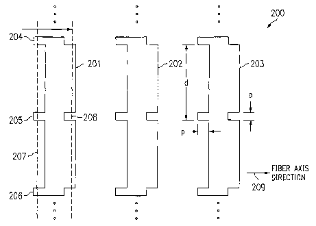
FIGURE 2 depicts an example of'feathering' of a mask 200, wherein each bar
201, 202, 203 has three pixels shifted, e.g. 204, 205, 206 in a direction that
is parallel
with the fiber axis direction 209. The pixel size is p, and by adding or
removing a single
pixel periodically with period d along the edge of a bar (transverse to the
axis of the
fiber), the effect of transverse averaging is to effectively sluft the edge of
the bar by a
distance equal to that of a pixel width reduced by its transverse duty cycle
(the width of a
single pixel divided by the number of pixels in the transverse period d, N = d
/ p). In
addition to the transverse averaging of the fiber core, the spot size limit of
the lithography
writing beam is generally larger than the address size, which can further
assist the
averaging effect. Based on this simple model for an ideal writing system, the
effective
shift of the bar edge from a single pixel p per transverse period d is ~z=p /
N = p2 /d.
Note that shifting a pixel can involve removing a pixel on one edge by itself,
and/or
adding a pixel to the opposite edge; or an entire line of pixels can be added,
removed,
and/or shifted over by one. In any event, shifting a pixel can result in
effectively moving
one or both edges of a bar, one 207 away from the bar, and the other 208 into
the bar.
For example, assume p = 5 nm, and allow for a minimum of only 1 pixel shifted
along the full extent of the fiber core (d =10 Vim), then the duty cycle of a
single shifted
pixel is 1/2000, and the minimum effective shift of the bar edge would be 0z =
p2 /d = 2.5
pm. This shift represents a small fraction of a pitch period in the fiber,
Oz/Ag ~ .0025 nm
/535 nm = 4.7 x 10-G, or a phase shift of 2~Oz / Ag = 2.9x10⁻⁵ radians. In
practice, to
avoid any dependency of the averaged shift on the actual relative position of
the fiber
core to the mask, it is preferable to have at least a few pixels over the core
diameter.
Even if the lithography tool has a larger pixel size p = 25 mn, then the
minimum duty
cycle increases to ~ 1/400 and the minimum shift is still only ~z = p2 /d = 63
pm, Oz/Ag
.063 nm / 535 nm = 1.2 x 10⁻⁴, or a phase shift of 7.3 x 10'4 radians. With
such small
incremental phase shifts it is possible to construct a chirped grating without
using any
rescaling or segmenting.
As an example, consider a linearly chirped grating with a bandwidth of 0.5 nm
and a chirp rate of 0.1 nm /cm of the Bragg wavelength along the fiber. For
this grating:
Ag(z) = Ago -az , for -2.5 < z < 2.5 cm, (3)
where a = 0.1/ 2nD = 0.035 nm / cm is the chirp rate, and Ago ~ 535 nm is the
average
pitch of the FBG. This can be approximated by a linear variation of the
inverse pitch of
the fiber grating
Ag(z)= Ago+az/A~o, for-2.5<z<2.5 cm, (4)
11
CA 02431234 2003-06-10
WO 02/061489 PCT/US02/00241
Such a linear chirp is produced by a quadratic variation in the phase of the
index
modulation,
n(z) =no+ h~ cos(2~cz / A go + ~g (z)),
where the chirp is given by
2~t (A g (z) - A ~o ) = dø~ (z) l dz ' (6)
and thus the required phase is
~g(z) = 2~caz2 / 2A go, for -2.5< z < 2.5 cm. (7)
= 3.8z2 radians
From Eq. (7) it is noted that the maximum rate of phase change is 18.9 rad /
cm at
the ends of this chirped FBG. Therefore, the phase variation over a single
pitch in the
fiber is 535 nm x 18.9 rad /cm =1.0x10⁻³ rad. As a result, the feathering
technique
described has adequate resolution to essentially continuously track the phase
of the chirp,
even where the phase varies most rapidly.
In practice, continuous tracking of the phase is not necessary. If one butt
couples
regions of equal and constant pitch, but each of which has a phase shift
according to Eq.
(7), then the grating response is adequate over the 0.5 nm bandwidth if ~z < 1
xmn.
However the periodic phase errors from this piecewise constant phase approach
lead to a
periodic side lobe structure which has a frequency spacing of 0.08 nm / ~z,
where Oz is
in cm. These results are shovcni in FIGURES 3A-3E. These FIGURES depict the
calculated reflectivity using grating segments with constant pitch, each phase
shifted
according to Eq. (7). FIGURE 3A depicts 500 p,m segment lengths. FIGURE 3B
depicts
125 ~,m segment lengths. FIGURE 3C depicts 62.5 p.m segment lengths. FIGURE 3D
depicts 31.3 ~.m segment lengths. FIGURE 3E depicts 31.3 gm segment lengths
with a
magnified scale. If 0z is smaller than ~30 gm, then the side lobes are
separated by ~ 25
rim, and can thus be pushed outside of the commonly used C-band of Erbium
doped
optical fiber amplifiers.
Whether the phase of the bar-space pattern is varied continuously or in a
discrete
fashion, the feathering technique allows the attainment of ~ pm resolution for
the
effective relative positions of the bars without varying the magnification
scale factor
and/or re-registering the lithography stage position. Thus, the Bar-Space pair
with m
pixels per transverse interval d shifted from one edge of the bar to the other
edge as BSm,
12
CA 02431234 2003-06-10
WO 02/061489 PCT/US02/00241
will have an effective positional shift of m~z, where 0z = p2 /d and m can
vary from 0 up
to N = d / p. When all the pixels have shifted to the opposing edge, this
results in the
conventional shift of a single pixel, and then shifting can be cyclically
continued over
again. Given a desired phase function for the grating as in Eq. (7), the
positional shift 8
of each bar can be defined as a fiuzction of z,
S(z) _ ~g(z)A go 12~t
The number of pixels shifted at each bar position is then given by
m(z) = 8 (z) l ( p2 l d ) (9)
where m > d / p indicates that there is a complete shift of 8(z) / p pixels,
plus [m(z) mod d
/ p] pixels 'feathered' over the interval d. FIGURE 4 depicts an example of
cyclic
movement of the pixels from one edge of a bar to another across the mask. In
bar 401,
most of the pixels have already been shifted, e.g. only two remain, within the
periodic
interval d, where m=d/p-2. In this case, note that the effective shift is 0z =
m p2 /d. In
bar 402 an entire column of pixels has been moved from one edge to the other
and the
shifting is repeating, beginning with a single pixel being shifted, where m=1.
Hence, the
effective shift is ~z = p+m p2 /d. The effect of writing beam size and other
effects in the
lithography tool may cause the variation of effective shift 8(z) versus the
number of
shifted pixels m to deviate from the simple linear relationship expressed in
Eq. (9). For
example, the effect of resolution will be very different for two pixels that
are adjacent
versus two which are not. As a result one may be required to calibrate this
effect in some
way to appropriately select m(z).
If this scheme is used to continuously modify the phase (position) of each
bar,
then the grating will have the pattern
BS'n' BS"'2 . . . BS"'~ ( 10)
where m; is given by Eq. (9) evaluated at the position of each bar. If phase
changes only
over an interval corresponding, for example, to j repetitions of the Bar-Space
period, the
grating would have the pattern .
BS'n~, J [ BSn'Z, J . . . [ BS'n~ ] j , 1 1
where ~BS"'~,~ indicates j repetitions of the BSn'~ pattern. Either changing
the phase
continuously or over a given interval, the positional resolution is determined
by the limit
of the feathering technique 0z = p2 / d.
13
CA 02431234 2003-06-10
WO 02/061489 PCT/US02/00241
This technique is easily adapted to incorporate discrete phase shifts. If at
any point
along the fiber a discrete phase shift 0 ~ is required, one simply
incorporates a gap of the
appropriate width
~ = D ~A ~o / 2~ (12)
at the location desired. The only limitation will be the resolution limit,
i.e. it is required
that 8 » Oz = p2 / d . Note, however, that for the special case where the
phase shift is an
integral or rational fraction of ~t, a shift corresponding to a full pixel
width without
feathering may suffice exactly. For example, if a ~ shift is desired in the
FBG, then
8 = A g / 2 = A ", / 4. Hence, if the basic BS period is a multiple of 4
pixels, a gap of l/4 of
the BS period on the mask will be an integral number of pixels and will
generate exactly
the desired ~/2 phase shift in the mask, and ~t shift in the FBG.
Note that the use of these new techniques may be combined with the currently
practiced resealing method to achieve a significant reduction in the number of
stitching
errors. For example, if a chirped grating requires many phase shifts every
millimeter,
then the current art would require repositioning every shift. This leads to
many more
stitching errors than are required for writing a simple chirped grating (for
which resealing
is needed only every ~ 1 mrn). One can therefore use pixel shifts as described
above to
generate phase shifts at whatever frequency is required (e.g. every 50 Vim),
yet rescale
only according to that which is required by the chirp (every ~ 1 mm). In this
case each
segment would have the general fornz
SBgk = [B,fm~~ ~J~x Slk[BS~nz~ ~Jxk S2k ~...[BS~n~~ ~J~x ~Jk (13)
where 8ik axe the required phase shift gaps as per Eq. (12). Each segment
pattern Segk
could then be scaled by an arbitraryfactor Sk, as in the currently practiced
art. This would
then accomplish an arbitrary number of phase shifts while maintaining the
number of
resealing typically used for a conventionally chirped FBG. However, since the
resealing
will still lead to stitching errors, it would generally be preferred to use
the feathering
technique over the entire pattern without any resealing.
FIGURE 5 depicts an example of a system configured to use the inventive maslc
502 to record a FBG onto the core of a fiber 504. A light source 501, e.g.
ultraviolet
laser, would provide the input beam. A phase mask 502, constructed as
described above,
separates the light beam into two first order diffracted beams, which project
out of the
plane of the FIGURE. These two interfering 1St order diffracted beams form the
grating
within the fiber core.
14
CA 02431234 2003-06-10
WO 02/061489 PCT/US02/00241
Focusing lens 506 is used to focus the light through the mask and onto the
fiber
core. This allows a larger portion 503 of the mask 502 to be illuminated by
the light
source beam; larger in the direction that is transverse from the fiber axis.
This, in turn,
allows for more illuminated pixels on a given bar to be focused and thus
averaged in the
formation of the grating within the fiber core, which provides even greater
resolution.
That is, if the light beam, which is focused onto the approximately 10 ~,m
size of the fiber
core, has a much larger size when it passes through the mask, the period d can
be much
larger than 10 Vim. Thus the beam can have many periods d witlun the beam, so
that good
averaging is maintained. The number of pixels, N = d/p, which are effectively
illuminated and focused onto the core of the fiber, can be larger and
therefore better
resolution (a smaller effective shift of a single pixel p/N = p2/d) can be
obtained. Since
the focusing need only be in the direction orthogonal to the fiber axis, it
may be
preferable to have the focusing lens system comprise at least one cylindrical
lens.
FIGURE 6 depicts another embodiment of a system configured to use the
inventive mask 602 to record a FBG onto the core of a fiber 604. As in FIGURE
5, a
light source 601, e.g. ultraviolet laser, would provide the input beam. A
phase mask 602,
constructed as described above, separates the light beam into two first order
diffracted
beams, which project out of the plane of the FIGURE. Beam focusing lens 606 is
used to
focus the light through the mask and onto the fiber core. In this embodiment,
the
arrangement is supplemented by an optical imaging system between the mask and
fiber,
which may consist of one or more lenses 607. This optical system images the
two first
order diffracted beams emanating from the mask onto the fiber core to form the
FBG
within the core. A stop 605 may be used to block a zero order beam, if
present,
emanating from mask 602. Note that if there is no zero order beam, then a stop
does not
need to be used. Note that the imaging is only necessary for the direction
along the fiber
(out of the plane of FIGURE 6). Therefore the one or more imaging lenses 607
need only
be cylindrical, oriented to focus rays going out of the plane of the page. If
lens or lenses
607 are cylindrical and oriented as described, then the beam focusing lens or
lenses 606
can be cylindrical and orthogonally oriented, and then can be independently
adjusted to
focus the beams on the fiber core without being affected by the one or more
imaging
lenses 607.
Note that the invention has been described in terms of forming a phase mask.
However, the inventive feathering may also be used in forming an absorption
mask,
wherein the feathering is printed onto the surface of the substrate as dark
bars. These bars
would have different transmission or transmittance than the spaces. Such a
mask can be
used to form an interference pattern by diffracting the light of an incoming
beam into two
beams, similarly to that of a phase mask.
CA 02431234 2003-06-10
WO 02/061489 PCT/US02/00241
Although the present invention and its advantages have been described in
detail, it
should be understood that various changes, substitutions and alterations can
be made
herein without departing from the spirit and scope of the invention as defined
by the
appended claims. Moreover, the scope of the present application is not
intended to be
limited to the particular embodiments of the process, machine, manufacture,
composition
of matter, means, methods and steps described in the specification. As one of
ordinary
skill in the art will readily appreciate from the disclosure of the present
invention,
processes, machines, manufacture, compositions of matter, means, methods, or
steps,
presently existing or later to be developed that perform substantially the
same function or
achieve substantially the same result as the corresponding embodiments
described herein
may be utilized according to the present invention. Accordingly, the appended
claims are
intended to include within their scope such processes, machines, manufacture,
compositions of matter, means, methods, or steps.
16