Note: Descriptions are shown in the official language in which they were submitted.
CA 02431340 2005-10-13
2,431,340
NETWORK TRANSCEIVER FOR EXTENDING THE BANDWIDTH
OF OPTICAL FIBER-BASED NETWORK INFRASTRUCTURE
Field of Invention
10
This invention relates to time division multiplexing networks, such as an
Ethernet (a trade-mark) infrastructure, and more particularly, this invention
relates to expanding the bandwidth of an optical fiber-based time division
multiplexed network infrastructure.
Backctround of the Invention
Time division multiplexing networks, such as an Ethernet infrastructure,
are increasingly becoming important in the technology of today. The bandwidth
used on such networks require periodic increases as more users are added,
larger files are transferred, and more complicated programs run on servers and
workstations. The infrastructures vary on design, and include 10 Mb/S (10 Base-
T), 100 Mb/S (100 Base-T), and 1,250 Mb/S (1,000 Base-T). Typically, to
increase an Ethernet bandwidth, the data rate was increased, such as operating
from an original 10 Base-T system to a 100 Base-T system.
It has been found that increasing the data rate transmission in mul6mode
fiber is severely limited by modal dispersion. One method currently used
CA 02431340 2005-10-13
2,431,340
- 2-
for combating the modal dispersion degradation is to use newly developed
multimode fiber designs, such as InfiCore (a trade-mark), which requires
replacing existing fiber infrastructures. This can be expensive, especially in
some metropolitan areas where it is cost prohibitive to add additional or
replace optical fiber lines. For example, in a major metropolitan area, to
replace or add fiber lines would require obtaining many permits from
municipal authorities and many worker hours in replacing or adding additional
cables under existing streets. Also, prior art wavelength channels in some
multiplex schemes have been wide, at about 3,000 gigahertz.
Summary of the Invention
It is therefore an object of the present invention to expand the bandwidth
of an existing optical communications network without the drawbacks of the
prior art.
The present invention is advantageous and builds on existing network,
e.g., Ethernet components, and existing fiber infrastructure. The system
technical approach is extensible to higher channel counts and higher data
rates to achieve higher aggregate information capacity.
In one aspect of the present invention, a multimode wavelength division
multiplexing (V11DM) network transceiver includes a plurality of optical
transmitters for transmitting optical communications signals along respective
signal paths. A multiplexer is operatively connected to each optical
transmitter and receives the optical communications signals and multiplexes
the optical communications signals into multimode wavelength division
multiplexed optical communications signal having wavelength channel
CA 02431340 2003-06-05
WO 02/089380 PCT/USO1/46543
-3-
spacings less than about 1,000 gigahertz. A
demultiplexer receives a multimode wavelength division
multiplexed optical~communications signal and
demultiplexes the signal into a plurality of
demultiplexed optical communications signals. A
plurality of optical receivers are each matched with a
respective optical transmitter and receives and detects
a respective demultiplexed optical communications
signal.
In one aspect of the present invention, the
optical receiver Comprises .a PIN Detector. The PIN
detector comprises an InGaAS PTN detector. It also
includes a transimpedance amplifier. In yet another
aspect of the present invention, the transmitter
25 comprises a distributed feedback laser and a
thermoelectric cooler and controller circuit.
In still another aspect of the present
invention, an attenuator is positioned within a signal
channel between each optical transmitter and the
multiplexer. A single mode optical fiber defines a
signal channel between the attenuator and the optical
transmitter, and a multimode optical fiber defines a
signal channel betweeri~the attenuator and multiplexer.
A transceiver is electrically connected to each optical
transmitter and matched optical receiver for receiving
and transmitting an optical communications signal. The
transceiver is operative at a first wavelength band and
the optical transmitter and matched optical receiver
are operative at a second wavelength band, which is
upconverted from the first wavelength band.
In yet another aspect of the present
invention, the network transceiver includes physical
sublayer chip circuits operatively connected to a
plurality of optical transmitters and matched optical
receivers. An electrical interface is operatively
CA 02431340 2003-06-05
WO 02/089380 PCT/USO1/46543
-4-
connected to the physical sublayer chip circuit. The
electrical interface comprises a plurality of RJ-45
jacks Ethernet 1,000 Base-T connection. A
serial/deserializer (SERDES) circuit is operatively
connected to an optical transmitter and matched optical
receiver. A switch circuit is operatively connected to
the serial/deserializer circuit and a physical sublayer
chip circuit and electrical interface are operatively
connected to the switch circuit.
In one embodiment of the present invention, a
multiport network hub includes a plurality of
transceiver boards, each having a network interface
connection to a network and a switch circuit
operatively connected to the network interface. At
least one optical transmitter receives signals from the
network on the network interface and transmits optical
communications signals. At least one optical receiver
is matched with the at least one optical transmitter
for receiving and detecting an optical communications
signal and generating a signal to the network via the
network. interface. A processor is operatively
connected to the switch circuit for~controlling same.
A bus interconnects each processor and a wavelength
division rnultiplexer is operatively connected to each
optical transmitter for multiplexing the optical
communications signals into a multimode wavelength
division multiplexed optical communications signal. A
demultiplexer is operatively connected to each optical
receiver and receives and demultiplexes multimode
wavelength division multiplexed optical communications
signal into a plurality of demultiplexed optical
communications signals.
A method is also disclosed of expanding the
bandwidth of an existing optical communications network
by transmitting optical communications signals from a
CA 02431340 2003-06-05
WO 02/089380 PCT/USO1/46543
-5-
plurality of optical transmitters positioned along
respective signal channels. The optical communications
signals are multiplexed into a multimode wavelength
division multiplexed optical communications signal. A
demultiplexer demultiplexes a multimode wavelength
division multiplexed optical communications signal into
a plurality of optical communications signals along
respective signal channels that are receiving detected
signals with optical receivers that are matched with
the optical transmitters.
Brief Description of.the Drawings
Other objects, features and advantages of the
present invention will become apparent from the
detailed description of the invention which follows,
when considered in light of the accompanying drawings
in which:
FIG. 1 illustrates an exemplary Ethernet
infrastructure having a multimode WDM network
transceiver of the present invention connected to
Ethernet servers and respective Ethernet switches.
FIG. 1A illustrates a plurality of Ethernet
switchers connected via multimode optical fiber to the
multimode WDM network transceiver of the present
invention as used in an Ethernet infrastructure.
FIG. 2 is a schematic drawing of an exemplary
Ethernet infrastructure and showing a use of the
multimode WDM network transceivers of the present
invention.
FIG. 3 is a high level block diagram showing
basic components of an example of a multimode WDM
network transceiver of the present invention.
FIG. 4 is a high level block diagram of a
transmitter module that can be used in the multimode
WDM network transceiver of the present invention.
CA 02431340 2003-06-05
WO 02/089380 PCT/USO1/46543
-6-
FIG. 5 is a high level block diagram of
another example of a multimode WDM network transceiver
of the present invention, which allows multiple
channels to be combined into a single multimode fiber
allowing increased data throughput on an existing local
area network (LAN) architecture.
FIG. 6 is a block diagram of another example
of a multimode WDM network transceiver as an exemplary
Ethernet converter, which allows a multiport 1,000
base-T connection and conversion to a gigabyte WDM
signal.
FIG. 7 is a block diagram of another example
of a multimode WDM network transceiver of the present
invention and showing an exemplary Ethernet hub that
implements direct conversion from 10/100 copper to
gigabyte wavelength division multiplexed signals.
FIG. 8 is a block diagram of the Ethernet hub
of FIG. 7, showing a network application on various
floors of a building.
Detailed Description of the Preferred Embodiments
The present invention will now be described
more fully hereinafter with reference to the
accompanying drawings, in which preferred embodiments
of the invention are shown. This invention may,
however, be embodied in many'different forms and should
not be construed as limited to the embodiments set
forth herein.' Rather, these embodiments are provided
so that this disclosure will be thorough and complete,
and will fully convey the scope of the invention to
those skilled in the art. Like numbers refer to like
elements throughout.
An apparatus and method of the present
invention includes a multimode wavelength division
multiplexing (WDM) network transceiver that allows the
CA 02431340 2003-06-05
WO 02/089380 PCT/USO1/46543
bandwidth extension of an optical fiber-based
wavelength division multiplexed network infrastructure,
such as an Ethernet infrastructure as a non-limiting
example, using multimode wavelength division
multiplexer technology. Throughout this description,
the apparatus and method of the present invention is
described relative to an Ethernet infrastructure. The
invention, however, can be applied to any network
infrastructure having time division multiplexed
transparent capabilities. Ethernet is only one type of
format that can be used in the present invention.
As noted before, prior art practices increase
the Ethernet bandwidth by increasing the data rate of
signals within the infrastructure, such as 10 Mb/S (10
base-T), 100 Mb/S (100 base-T), and 1,250 Mb/S (1000
base-T). Increasing the data rate transmission in
multimode fiber is limited; however, by modal
dispersion. Placing additional lines in some areas is
cost prohibitive. For example, it is cost prohibitive
to add additional optical fiber lines under a street in
a crowded metropolitan area. The present invention
advantageously increases the. network bandwidth, e.g.,
Ethernet bandwidth, using multimode fiber-based
wavelength division multiplexing techniques by building
on the existing network components and existing fiber
infrastructures. It is extensible to higher channel
counts and higher data rates to achieve higher
aggregate information capacity.
FIG. 1 illustrates a network 10 as an
Ethernet infrastructure, having personal computers 12
connected via regular network wiring connections 14,
known to those skilled in the art, to 1.25 Gb network,
e.g., ~thernet, switches 7.6. The Ethernet
infrastructure 10 includes servers as illustrated at
18, where three 1.25 Gb servers are shown. The servers
CA 02431340 2003-06-05
WO 02/089380 PCT/USO1/46543
_g_
18 are operatively connected to the multimode WDM
network transceiver 20 of the present invention and
operatively connected to existing multimode optical
fiber 22 and a second multimode WDM network transceiver
20a, which is operatively connected to the 1.25 Gb
network, e.g., Ethernet, switches 16. Although the
term "multimode WDM network transceiver 20" is used
throughout the description, it should be understood
that in the context of the Ethernet infrastructure 10
of FIG. 1, the transceiver is an exemplary multimode
wavelength division multiplexed Ethernet transceiver
that is operative from about 1.25-20 Gb/s. It can be
used for various products as further explained below,
including but not limited to, an Ethernet transceiver,
an Ethernet converter and multiport Ethernet hub. .
FIG. 1A is a block diagram showing another
example of the multimode WDM network transceiver 20
that operatively connected to 26 different Ethernet
switches 24, via 1.25 Gb/s Ethernet multimode fiber 26
and to the existing optical multimode link fiber 2S for
transmitting and receiving data signals. The
transceiver 20, in one embodiment, is formed as a
separate module that is operatively connected to
existing Ethernet and other network components. It is
operative with up to about 16 channels of 1.25 Gb/s,
200 GHz through 400 GHz spaced WDM optical
communications signals. The system is operative with
short haul local area network on 62.5 micrometers or 50
micrometer multimode fiber or single mode fiber. The
multimode WDM network transceiver can be formed on one
printed wiring circuit board (or other chassis or other
known type of circuit board), and inserted into a
conventional 19" or similar rack. The transceiver can
be rack mounted in a 5U ventilated chassis or slice
CA 02431340 2003-06-05
WO 02/089380 PCT/USO1/46543
-9-
apparatus, as known to those skilled in the art. The
transceiver 20 is operative at different wavelengths,
and particularly the ITU grid of 1550..XXX nanometer
wavelengths known to those skilled in the art. The
transceiver 20 is Ethernet compatible and is also
transparent to other time division multiplexing (TDM)
formats, such as 100 base-FX and similar existing
standards.
The present invention advantageously allows
2-16 channels of Gb Ethernet to be combined into a
single multimode fiber, allowing up to 20 Gb/s data
throughput on an existing LAN structure. In one aspect
of the present invention, it is scalable to 16 channels
and uses a multiplexer with a standard commercial off-
the-shelf (COTS) 1x16 coupler, and a demultiplexer
filter based on a bulk defraction grating and 50 or
62.5 micrometer multimode fiber. It advantageously
reuses the existing multimode link fiber and compatible
with existing standards and reuses existing equipment.
It has a greater reach with a direct interface to
existing equipment and "as needed" modular channel
upgrades.
The transceiver 20 of the present invention
uses transmitters, such as 2.5 Gb/s directly modulated
distributed feedback (DFB) laser modules with
integrated thermoelectric cooler (TEC), temperature
control, optical power control and laser driver
circuitry. The receivers can use 2.5 Gb/s, InGaAS PIN
diodes with integrated transimpedance amplifier (TIA),
post amplifier, positive emitter coupled 1~gic (PECL)
driver and signal detect. The transceiver, in one
aspect of the present invention, has an interface to
existing 1.25 Gb Ethernet backbone with 850 nanometer
transceivers and ST couplers for multimode fiber
connection.
CA 02431340 2003-06-05
WO 02/089380 PCT/USO1/46543
-10-
Although not illustrated in detail, the
transceiver 20 could be incorporated in a separate
housing, such as a module box, with front panel light
emitting diode (ZED) indicators used for each channel,
such as an 850 nanometer signal detect (green), a WDM
signal detect (green), a WDM launch power (red), and
WDM wavelength error (red). The power supply could be
a 200 watt supply with 3.3 volt, 5 volt and 12 volt
outputs with thermoelectric coolers at 3.3 volts and 11
amps. The receivers and transceivers could be
operative at.3.3 volts and 1.5 amps-with laser control
circuits at 5 volts and 0.2 amps and ventilation fans
with 12 volts and 0.4 amp operation. Although the
above specifications are only non-limiting examples,
they give a detailed example of the type of components,
circuits, and specifications operative with the present
invention.
FIG. 2 illustrates an example of how the
transceiver 20 is operative with Ethernet switches 30
having 1,000 BSX ports with one built in and two add-
ons that are operatively connected to 10/100 megabyte
workstations 32 via 100.megabyte copper interconnects
34, as part of an Ethernet infrastructure. Another
Ethernet switch 36 is connected to 1000 Mb servers 38
and a second transceiver 20a via 1000 BSX multimode
fiber 40.
FIG. 3 illustrates a multimode WDM network
transceiver 20 that can be incorporated onto one
circuit board 42 and operative at 10 Gb/s. The
transceiver 20 can be operative up to 20 Gb/s or more
when additional components are added. The board 42 is
only shown with sufficient components to allow 10 Gb/s
data throughputs, as a non-limiting example.
CA 02431340 2003-06-05
WO 02/089380 PCT/USO1/46543
-I1-
The rear interface 44 to the existing link
fiber is positioned at the rear of the board or module
box and connects to the multimode fiber via a receive
port 46 and transmit port 48, as illustrated. A front
interface 50 to existing equipment allows fiber to be
brought in and out as a plug-in to the front of the
board or module box. The front interface 50 is
compatible to existing equipment, as known to those
skilled in the art, such as standard Ethernet
equipment. The front interface 50 includes the
transmit and receive fiber connectors 52,54 (or ports)
that interconnect existing optical fiber into 850
nanometer transceivers 56, as a non-limiting example.
Eight 850 nanometer transceivers 56 are illustrated to
allow 10 Gb/s multimode WDM network data transfer as
one example of the present invention. In a 20 Gb/s
multimode WDM network transceiver board,.42, as an
example, sixteen 850 nanometer transceivers would be
used and would connect as a direct interface to
existing equipment.
The transceivers 56 are connected via a 50
ohm, AC coupled differential, ZV positive emitter
coupled logic (PECZ) connection 58 to a WDM integrated
optical transmitter module 60, operative in the 1500.XX
nanometer wavelength band. A receiver 62 is preferably
formed as an integrated PIN receiver, including InGaAS
PIN diodes. It includes a transimpedance amplifier
(TIA) and postamplifier operative therewith. The WDM
integrated transmitter module 60 is connected via
single mode fiber 64 to an attenuator 66, which in
turn, is connected with single mode fiber 68 and
operative with a combiner/multiplexer 70, which
multiplexes the optical communications signals from the
single mode fiber to transmit over one multimode fiber
CA 02431340 2005-10-13
2,431,340
- 12-
at the transmit port 48. The integrated PIN receiver 62 is connected to
multimode fiber 72, which is connected to a filter 74 that is an 8 or 16
channel
demultiplexer (8 channel illustrated), which filters out the different
wavelengths received on the existing link fiber into the separate wavelengths
by techniques known to those skilled in the art.
FIG. 4 illustrates a block diagram of a WDM integrated transmitter module
60 that can be used in the present invention and is operative at the
wavelengths, such as illustrated in FIG. 3. The optical transmitter 60
includes
a standard optics, using circuit 89 that acts as a laser driver and control
circuit, and an appropriate temperature control circuit 82 and monitor and
alarm circuit 84. Various output/input ports 86 are used for operation and
interconnection. The transmitter 60 can be formed as a distributed feedback
laser circuit.
The optical transmitter 60 can be operative on a single silicon integrated
circuit with a back facet diode as a feedback element with a closed loop
control system. Such types of devices are manufactured and sold by various
companies, including Nortel Networks Corporation (a trade-mark) as a 2.488
Gb/s WDM transmitter module. The optical transmitter can include inputs that
are AC coupled with 100 ohm differential impedance and a voltage swing for
PECUECL. The laser device can be a distributed feedback laser with the
optical isolation, laser drive, automatic laser power control and monitoring
function with the thermoelectric cooler, to maintain constant laser
temperature
and wavelength. The transmitter can include standard microprocessor based
n control circuits having an optical via a
CA 02431340 2003-06-05
WO 02/089380 PCT/USO1/46543
-13-
single mode pigtail that can be fitted with various
single mode optical connectors, as known to those
skilled in the art.
The various output/input ports 86 and
associated circuit functions include a transmitter
disable for enabling and disabling the laser and a
laser bias current monitor that provides an-analog
voltage output for laser bias current, indicating a
change of laser threshold as the laser ages. A bias
out-of-limits alarm can be activated when there is a
failure of the laser or when the laser EOL
characteristics are about to be met. Temperature
monitoring provides a voltage output for a laser
submount temperature and a temperature alarm can
provide an appropriate alarm with threshold. The
modulation input allows amplitude modulation for
wavelength tagging while appropriate power supply
inputs can be filtered.
FIGS. 5-8 illustrate three different
embodiments of the present invention. FIG. 5
illustrates a 1,000 Base-SX (or LX) to 10 Gb/s (or 20
Gb/s) Ethernet transceiver 100, where short wavelength
laser transceivers or multimedia fiber support lengths
of 300 meters (using 62.5 micrometer multimode fiber)
or 550 meters (using 50 micrometer multimode fiber) can
be operable. 1,000 Base-LX long wavelength laser
transceivers can also be used for transmission
facilities. An SX or LX transceiver 102 is connected
via positive emitter coupled logic (PECL) circuit 104
to the transmitter module 60 having distributed
feedback laser and operative at a first wavelength and
to the InGaAS PIN receiver 62. Eight receivers and
transmitters are illustrated, and operative at eight
wavelengths Al to A8, which are operative on eight
CA 02431340 2003-06-05
WO 02/089380 PCT/USO1/46543
-14-
signal channels. The eight wavelength signal channels
and associated transmitters and receivers are connected
to the WDM multiplexes 70 and filter 74 as described
before with optical fiber connections for transmit and
receive ports. This example of the present invention
allows eight (or 16 if 16 transceivers are used)
channels of SX or LX Gb Ethernet to be combined into a
single, duplex, multimode fiber allowing 10 (or 20)
Gb/s data throughput on the existing local area network
(LAN) architecture.
FIG. 6 illustrates another embodiment of the
present invention using similar components, but showing
an eight port 1,000 Base-T to 10 Gb/s Ethernet
converter 110, which could be a 16 port 1,000 Base-T to
20 Gb/s Ethernet converter when 16 electrical input
channels and appropriate components are used. As
illustrated, the 1,000 Base-T Ethernet connection is
used with RJ-45 couplers 112 that are connected to
transformers (XFMR) 114 using circuit principles known
to those skilled in the art. The transformers 114 are
operative with quad gigabyte physical sublayer chips
116 (PHY) and a gigabyte medium independent interface
(GMII) circuit 118 to the quad gigabyte physical
sublayer chips (PHY) (PECL I/F) 120, as known to those
skilled in the art. The GMII interface 118 could
define independent parallel transmit and receive
synchronous data interfaces and allows a chip-to-chip
interface to mixed Media Access Control (MAC) and
physical sublayer components. The GMII interface 118
is operative with the pairs of quad Gb physical
sublayer components 116, 120, as illustrated. The
positive emitter coupled logic (PECL) quad gigabyte PHY
120 is operative with the transmitters 60, having the
CA 02431340 2003-06-05
WO 02/089380 PCT/USO1/46543
-15-
DFB laser modules, and operative with the InGaAS PIN
receivers 62, the filter/demultiplexer and multiplexer.
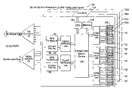
FIGS. 7 and 8 illustrate another embodiment
of the present invention forming a 96 10/100 port
Ethernet hub 130 having a 10 Gb/s uplink. As
illustrated, four separate transceiver boards 132a-d
are connected via a PCI bus 134, and operable with a
CPU 136 and memory unit 138 into a 10/100/1000 switch
device 139. The switch device is operative with the
octal physical sublayer chips (PHY) 140 and RJ-45 input
ports 142. The switch device 139 is operative with
gigabyte serializer/deserializer (SERDES) 144 and is
typically monolithically formed with clock recovery and
clock multiplication with multiple interfaces, back
plane, cables and optical modules. As known to those
skilled in the art, the SERDES 144 is also typically
formed as an application specific integrated circuit
(ASIC) transceiver core that provides for integrated,
ultra-high speed bidirectional point-to-point data
transmission over various impedance media. The SERDES
connects through the DFB transmitter 60 and PIN
receiver 62 of the type as described before, and into
the appropriate combiner/multiplexer and
demultiplexer/filter using the multimode fiber at
transmit and receive ports to form the 10 Gb/s port as
illustrated. . Thus, the hub allows direct conversion
from 101100 copper to 10 Gb/s WDM optical link.
FIG. 8 sows a network application with the
1,000 base-SX (4 ZX) to multi-gigabyte (10-20) Ethernet
transceiver of the present invention and showing on
floor one a server farm with floor 2, floor 3 and
floor 4 having various Ethernet hubs 130 of the present
invention connected to various workstations 146 as
illustrated.
CA 02431340 2003-06-05
WO 02/089380 PCT/USO1/46543
-16-
Many modifications and other embodiments of
the invention will come to the mind of one skilled in
the art having the benefit of the teachings presented
in the foregoing descriptions and the associated
drawings. Therefore, it is to be understood that the
invention is not to be limited to the specific
embodiments disclosed, and that the modifications and
embodiments are intended to be included within the
scope of the dependent claims.